EP0170525A2 - Entwurf einer Cache-Hierarchie zur Anwendung in einer Speicherverwaltungseinheit - Google Patents
Entwurf einer Cache-Hierarchie zur Anwendung in einer Speicherverwaltungseinheit Download PDFInfo
- Publication number
- EP0170525A2 EP0170525A2 EP85305453A EP85305453A EP0170525A2 EP 0170525 A2 EP0170525 A2 EP 0170525A2 EP 85305453 A EP85305453 A EP 85305453A EP 85305453 A EP85305453 A EP 85305453A EP 0170525 A2 EP0170525 A2 EP 0170525A2
- Authority
- EP
- European Patent Office
- Prior art keywords
- cache
- memory
- address
- map
- logical
- Prior art date
- Legal status (The legal status is an assumption and is not a legal conclusion. Google has not performed a legal analysis and makes no representation as to the accuracy of the status listed.)
- Granted
Links
Images

Classifications
-
- G—PHYSICS
- G06—COMPUTING OR CALCULATING; COUNTING
- G06F—ELECTRIC DIGITAL DATA PROCESSING
- G06F12/00—Accessing, addressing or allocating within memory systems or architectures
- G06F12/02—Addressing or allocation; Relocation
- G06F12/08—Addressing or allocation; Relocation in hierarchically structured memory systems, e.g. virtual memory systems
- G06F12/10—Address translation
- G06F12/1027—Address translation using associative or pseudo-associative address translation means, e.g. translation look-aside buffer [TLB]
- G06F12/1045—Address translation using associative or pseudo-associative address translation means, e.g. translation look-aside buffer [TLB] associated with a data cache
- G06F12/1063—Address translation using associative or pseudo-associative address translation means, e.g. translation look-aside buffer [TLB] associated with a data cache the data cache being concurrently virtually addressed
-
- G—PHYSICS
- G06—COMPUTING OR CALCULATING; COUNTING
- G06F—ELECTRIC DIGITAL DATA PROCESSING
- G06F12/00—Accessing, addressing or allocating within memory systems or architectures
- G06F12/02—Addressing or allocation; Relocation
- G06F12/08—Addressing or allocation; Relocation in hierarchically structured memory systems, e.g. virtual memory systems
- G06F12/0802—Addressing of a memory level in which the access to the desired data or data block requires associative addressing means, e.g. caches
- G06F12/0864—Addressing of a memory level in which the access to the desired data or data block requires associative addressing means, e.g. caches using pseudo-associative means, e.g. set-associative or hashing
Definitions
- This invention relates to improvements in computer memory systems, and more particularly to improvements in cache memories associated with computer memory systems.
- cache memories are small high speed memories used in modern, medium and high speed computers to temporarily hold those portions of the contents of main memory which are believed to be currently in use. Since instructions and data in cache memories can usually be referenced in 10 to 25 percent of the time required to access main memory, cache memories permit the execution rate of the machine to be substantially increased.
- a central processing unit (CPU) of a computer with a cache memory needs to spend far less time waiting for instructions and operands to be fetched and/or stored.
- main memory can be accessed in 300 to 600 nanoseconds, whereas information can be obtained from a cache in 50 to 100 nanoseconds. Since the performance of such machines is already limited in instruction execution rate by cache memory access time, the absence of any cache memory would produce a substantial decrease in execution speed.
- the success of cache memories has been explained by reference to the "property of locality".
- the property of locality has two aspects, temporal and spatial. Over short periods of time, a program distributes its memory references nonuniformly over its address space, and which portions of the address space are favored remain largely the same for long periods of time.
- This first property called temporal locality, or locality by time, means that the information which will be in use in the near future is likely to be in use already. This type of behavior can be expected from program loops in which both data and instructions are reused.
- the second property, locality by space means that portions of the address space which are in use generally consist of a fairly small number of individually contiguous segments of that address space.
- Locality by space means that the loci of reference of the program in the near future are likely to be near the current loci of reference.
- This type of behavior can be expected from common knowledge of programs: related data items (variables, arrays) are usually stored together, and instructions are mostly executed sequentially. Since the cache memory buffers segments of information that have been recently used, the property of locality implies that needed information is also likely to be found in the cache.
- Optimizing the design of a cache memory generally has four aspects:
- a cache memory 12 is ordinarily located between the CPU 13 and main memory 14.
- a secondary memory 17, such as a disk memory or the like, may also be included, connected to the main memory 14, as shown.
- the cache is addressed by real addresses, rather than virtual addresses.
- Examples of such computers are Amdahl 470, IBM 3081, Univac 1100/80, Honeywell 66/80, DEC VAX 11/780, 11/750. This is so, because these computers have multiple virtual address spaces, typically one per process.
- the operating system has its own virtual address space, separate from those used by the user processes.
- the same virtual addresses in different virtual spaces are mapped onto different physical addresses; on the other hand, different virtual addresses in different address spaces may be mapped onto the same physical address (in fact, this is the mechanism to allow sharing of information between two different virtual address spaces).
- the cache mapping mechanism becomes very complex, because the mapping mechanism also has to keep track of the address space. As a result, most of these older generation machines, first map'the virtual address onto the real address, before accessing the cache map. Usually, the virtual to real address translation process is time consuming, compared to the cache access time, and can become a performance bottleneck.
- the invention is particularly suitable for use in conjunction with computer systems such as those described in copending United States patent applications by Oxley et al, entitled “COMPUTER MEMORY SYSTEM”, serial number 630,476 , filed July 12, 1984, (attorney's docket number TI-9932), and by Thatte el al., entitled “COMPUTER SYSTEM ENABLING AUTOMATIC MEMORY MANAGEMENT OPERATIONS", serial number 630,478 , filed July 12, 1984, said applications being assigned to the assignee hereof, and incorporated herein by reference.
- a logical address cache is addressed by logical addresses generated by the CPU.
- a logical address is a pair, (r index), where "r" is the identification of a binding register and “index” is the index of a cell in the memory block bound to the binding register, r. Since none of the existing machines have the notion of logical addresses, they do not have caches that can be addressed by logical addresses.
- a logical address cache is addressed by logical addresses generated by the CPU.
- a logical address is a pair, (r index), where "r" is the identification of a binding register and “index” is the index of a cell in the memory block bound to the binding register, r.
- the cache system in accordance with the invention, is incorporated in the MMU, as described in said copending patent applications serial numbers 630,476 , and 630,478 , (attorney ' s docket numbers TI-9932 and TI-10599), can be implemented using a combination of two of the three mechanisms, the "logical address cache,” the “virtual address cache,” and the “real address cache. "
- the logical address cache allows cache accesses with the least time delay between the generation of a logical address by the CPU and the access to the addressed information from the cachet because the index in a logical address, (r index), is used to access the cache, and no translation from the logical to virtual address is required.
- the virtual address cache is addressed by virtual addresses obtained by translating logical addresses, and is computed from the logical address, (r index), by adding the index to the base virtual address stored in the binding register, r.
- the real address cache is addressed by real addresses, obtained by translating virtual addresses to real addresses.
- the real address is obtained by mapping the virtual addresses by an address translation mechanism, such as a page table.
- an address translation mechanism such as a page table.
- the real address cache suffers the worst time delay, as two address translations (the logical to virtual and the virtual to real address translations) are necessary before the real address cache can be accessed.
- a memory system for association with a CPU includes a memory management unit and a main memory.
- the memory management unit includes a binding register unit for interfacing the main memory to the CPU, and includes means comprising a plurality of binding registers for translating logical and virtual addresses between the CPU and the main memory.
- Each logical address includes a register pair (r,index), wherein "r" represents a binding register identifier and "index" represents an index of a cell in a memory block bound to the binding register indicated by "r".
- the binding register unit also includes a logical address cache to which logical addresses are applied, and responsive to which the logical address cache provides selected information cached therewithin.
- a virtual address cache provides selected information cached therewithin in response to virtual addresses applied to it.
- Means are provided for translating virtual addresses to real addresses for application to the main memory, and a memory management processor controls the operation of the memory management unit.
- the logical address cache comprises a cache memory, a cache map and a binding resolution map.
- the cache map, as well as the cache memory are divided into partitions, corresponding to the number of binding registers of the memory system.
- the binding resolution map receives a binding register identification of the contents of its entry point to a cache map partition and a cache partition. Means are also provided for indicating a cache hit or a miss upon the application of a logical address to the cache map.
- the virtual address cache comprises a cache memory and a cache map.
- the cache map receives a portion of the virtual address translated from the logical address and produces a cache hit or miss indication.
- the invention combines the advantages of logical and virtual address caches by presenting a cache hierarchy that consists of a logical address cache backed up by a virtual address cache.
- the goal is to achieve the performance advantage of a large logical address cache, and the flexibility and efficient use of cache capacity of a large virtual address cache, by employing a physically small logical address cache combined with a large virtual address cache.
- a logical address cache is also unique in its own right, as no known existing computers use a logical address cache.
- The.virtual address cache is backed up by the main memory.
- the cache hierarchy does not include a real address cache for reasons explained above.
- the logical and virtual address caches in accordance with the invention are shown in Figure 2 in the context of a computer system of the type described in the above referenced Oxley et al. patent application serial number (attorney's docket number TI-9932).
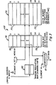
- a CPU 50 has an associated memory management unit (MMU) 52.
- the MMU 52 includes a memory management processor (MMP) 54 which controls the MMU functions, all as described in said Oxley et al. patent application.
- a binding register unit (BRU) 56, containing a plurality of binding registers 57 interfaces the CPU 50 and main memory 60 via respective data and logical address lines 61 and 62.
- the logical addresses L.
- the BRU 56 includes a logical address cache b8, in accordance with the invention, and the MMU itself includes a virtual address cache 85 between the BRU 56 and the main memory 60.
- the logical address cache 68 is addressed by logical addresses generated by the CPU 50.
- a logical address consists of an address pair, (r index), where "r" is the identification of a binding register and “index” is the index of a cell in a memory block bound to the binding register, r.
- the index part of the logical address is used to address the cache. (A virtual address is not required to address the logical address cache, avoiding the performance penalty inherent in the computation of a virtual address from the logical address.)
- the logical address cache 68 includes a cache memory portion 70 which is divided into a number of partitions 73.
- the number of cache partitions 73 equals the number of binding registers in the system, for example, 0 through 31, as shown.
- Each cache partition 73 is used to cache a memory block (or a portion of it), which is bound to one or more of the binding registers 57.
- a cache partition is associated with a binding register, and it caches the block bound to that binding register.
- a cache map 75 is provided which keeps a record of information present in the cache memory 70.
- the cache map 75 also is divided into partitions 78, each of which is associated with a respective partition 73 of the logical cache memory 70. Therefore, there are as many cache map partitions 78 as there are memory cache partitions 73, which equal the number of binding registers.
- Each cache map partition 78 indicates which locations of the cached block are present in the associated cache partition 73. If two or more binding registers are bound to the same block, they are associated with a single cache partition, the one that is caching that block.
- the binding resolution map 80 is provided to maintain a mapping between a binding register and the logical address cache partition associated with it.
- the map 80 has as many entries as there are binding registers in the machine. Thus, given the identification of a binding register, the binding resolution map 80 indicates the identification of a cache partition associated with the binding register, if any. Since a cache map partition 78 is associated with each cache partition 73 t given the identification of a binding register, the binding resolution map 80 also indicates the identification of a cache map partition 78 associated with the cache partition 73.
- a portion of the index part of the logical address applied to the logical address cache (the "set-id" portion) is contained in the cache map 75.
- the binding resolution map 80 When the binding resolution map 80 is addressed, the contents of the partition of the cache map indicated by the binding resolution map 80 is compared in a comparator 81 with the "element-id" portion of the index part of the logical address to indicate a cache hit or cache miss.
- This strategy of managing the logical address cache 68 by means of the binding resolution map 80 avoids multicache consistency problems that could arise were the cache design to use a separate cache partition for each binding register.
- An additional advantage of this strategy is that the cache design allows a "warm" cache to be created when a new binding is created for an existing block. When a new binding to an existing block is created, at least a-part of the existing block is present in the cache partition associated with the binding register to which the existing block is already bound. Thus, during the process of binding, a different binding register to the existing black, the new binding register is associated with the same cache partition in which at least a part of the existing block is present.
- binding register number 3 For example, if a block is already bound to a binding register, say binding register number 3, then the third entry of the binding resolution map would indicate the third cache partition to be caching the block. If a new binding to this block is then created in another binding register, say binding register number 5, then the fifth entry of the binding resolution map would indicate the third cache partition. This effectively creates a warm cache for binding register 5.
- An alternate strategy of managing the logical address cache is to assign a separate cache partition for each binding register.
- a block bound to multiple binding registers will exist in different cache partitions at the same time.
- An update of one partition would make the other partitions caching that block out dated, giving rise to multicache consistency problems.
- This strategy is of secondary preference, because it raises problems of multicache consistency.
- an example of the logical address cache 68 can be as follows.
- the index specified in a logical address can be viewed as consisting of three fields, namely, the word id, set id, and element id. This is illustrated in Table 1. (An index is assumed to be 32 bits in width.)
- the word identification (specified by the w least significant bits in the offset) specifies a word in a cache line consisting of 2w words.
- a line is the unit of data transfer between the cache and the backing store. A line is transferred between cacne and backing memory to serve a cache miss.) If a line contains only a single word, w will be 0. Typical values for parameter w are 0, 1, and 2, which will result into a line size of 1, 2, and 4, respectively.
- the next s bits in the offset specify the set id. If a fully associative mapping is followed, s will be 0.
- the set s identification specifies a set out of the total 2 possible sets. Typical values for parameter s, are 1, 2, or 3, which will result into a set size of 2, 4, or 8 lines, respectively.
- the last parameter, element id really specifies how many lines of the backing memory are mapped in each set.
- the example will also be used to illustrate the details of cache mapping and operation of the logical address cache.
- the Write-through policy (discussed below) is assumed.
- the design parameters of the cache are given below.
- the cache is made up of high speed static RAMs or a register file.
- the cache controller consists of a cache map 75 t a binding resolution map 80, and associated control logic (not shown).
- the cache map 75 contains 32 partitions, each managing a fixed size cache partition of 4 lines. Thus, each cache partition has 4 entries, and each entry is at least 29 bits wide. It should be noted that the size of each cache map partition matches the number of sets, and the width of each entry in a cache map partition is at least that of the element identification. The entries may have additional bits to record various control information.
- the binding resolution map 80 contains 32 words, each of 5 bits. This map is addressed using the binding register identification, r, of a logical address (r index), as the address. The 5-bit contents of the word thus addressed indicates the- identification of the partition of the cache map as well as the identification of the cache partition to be used.
- the indicated cache map partition is addressed by means of the set-id, i.e., by the (2:1) bits of the index.
- the contents of the cache map partition thus addressed are compared with the eiement-id, i.e., with bits (31:3) of the index. If the comparison indicates a match, there is a cache hit, otherwise a cache miss.
- the cache partition is also addressed by means of the set-id, i.e., by the ⁇ 2:1> bits of the index. If there is a cache hit, output of the cache partition indicates the output of the logical address cache.
- the cache output contains a line of two words. The word from the line is selected by using the word-id, which is bit ⁇ 0> of the index.
- the primary source of accesses to the logical address cache 68 is the CPU 50.
- the MMP 54 also accesses the logical address cache.
- the MMP 54 moves memory blocks from the OLDSPACE to the NEWSPACE in the virtual address space (OLDSPACE and HEWSPACE are described in detail in copending patent application by Bartley et al, entitled COMPUTER MEMORY SYSTEM WITH PARALLEL GARBAGE COLLECTION INDEPENDENT FROM AN ASSOCIATED USER PROCESSOR, serial number 636,187 , filed July 31 1984, (attorney's docket number TI-9928), assigned to the assignee hereof and incorporated herein by reference.
- the block Since the block is moved in the virtual address space, and not in the logical address space, the block itself need be moved only in the virtual address cache 85, described below, and not in the in the logical address cache 68. This is an advantage of the logical address cache over the virtual address cache.
- Any pointers to the block being moved, which may exist in other blocks must be updated in both caches. If a block holding a pointer to a moved block is in_the logical address cache, the cache location holding this pointer must also be updated with the new pointer (i.e., the new virtual address of the moved block).
- the MMP 54 knows the virtual address of the source block holding the pointers to a moved block.
- the MMP 54 searches the binding registers 57 to find out if any register(s) is bound to a source block. This search can be performed at a high speed if there is associative search hardware support (not shown) for the binding registers 57.
- the MMP 54 accesses the logical address cache partition associated with the binding register (bound to the source block) using the index corresponding to the word that contains the old pointer. If that word is in the cache partition, the MMP 54 updates the word using the new virtual address of the moved block. It is expected that most blocks will have only a few outstanding pointers to it in other blocks. So the MMP 54 may have to update only a few pointers in the logical address cache, only if the source block happens to be in the logical address cache 68.
- the logical address cache 68 should be implemented close to the binding registers 57 to avoid performance loss, because cache partitions are closely associated with binding registers. Similarly, the control of the logical address cache 68 is closely linked with that of the binding registers 57. If the CPU 50 is implemented with very large scale integrated (VLSI) technology, it is anticipated that the binding registers 57 and the logical address cache 68 will also be implemented on the same CPU VLSI chip (not shown). Because of space limitations such a chip is expected to accommodate only a small to moderate size logical address cache. Expected cache size permitted by current estimates of chip area is about 256 words, i.e., 8 words per cache partition assuming 32 binding registers in the machine. As the technology progresses.
- VLSI very large scale integrated
- the cache size is expected to increase to as much as 1,024 words; however, this would still be a moderate size cache.
- a drawback of logical address cache imposed by technological restrictions is its small size, which may partly reduce its inherent speed advantage due to poor hit ratio attributed to small size.
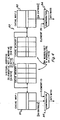
- a virtual address cache 85 is provided between the binding register unit 56 and the main memory 60.
- the virtual address cache 85 is illustrated in Figure 4.
- the logical address generated by the CPU 50 i.e., the (r, index) pair, is used to calculate the virtual address shown at the top of the figure by adding the virtual address stored in the binding register r of the binding register set 57 t to the index.
- the resulting virtual address is used to access the virtual address cache 85.
- This calculation entails reading of virtual address from the binding register r first, followed by the addition of the virtual address to the index.
- the entire calculation of the virtual address is expected to take at least 60 nanoseconds (20 nanoseconds for reading the binding register, and 40 nanoseconds for adding the virtual address read to the index), disadvantageously increasing the cache access time by at least 60 nanoseconds.
- the virtual address cache 85 there are some advantages of the virtual address cache 85.
- the entire cache is available for each binding register, i.e., full cache capacity can be exploited, and there is no restriction on sharing cache capacity among different binding registers. This is in contrast to the logical address cache partition scheme, which may show poor performance or inefficient use of cache capacity when there is a severe mismatch between the size of memory block being cached and the size of the cache partition.
- virtual address cache is its simpler control mechanism compared to that for the logical address cache.
- LSI chips such as Texas Instruments TMS 2150 cache controller chip
- a cache controller for the virtual address cache can be constructed to manage a fairly large size ⁇ 16 K words) virtual address cache.
- Table 2 summarizes the advantages and disadvantages of logical and virtual address caches.
- the virtual address cache 85 is addressed by the virtual address developed in the BRU 56.
- the virtual address is defined for purposes herein to have three fields, viz., the word id, the set id and the element id, for the purpose of virtual address cache access.
- the design parameters of the cache are given below.
- Each set of the two-way set-associative cache consists of 8 K words.
- the cache is made up of high speed static RAMs.
- the cache controller consists of cache maps and associated control logic.
- Each map contains 2,048 entries, each at least 19 bits wide. It should be noted that the cache map size matches the number of sets, and the width of each entry is at least that of the element id. The entries may have additional bits to record-various control information.
- Both cache maps 90 and 91 are addressed by means of the set-id, i.e., by the ⁇ 12:2> bits of the virtual address.
- the contents of both cache maps thus addressed are compared with the element-id, i.e., with bits ⁇ 31:13) of the virtual address in respective comparators 94 and 95. At most one comparison is expected to indicate a match, resulting into a cache hit; if neither comparison indicates a match, then there is a cache miss.
- both sets of the cache are also addressed by means of the set-id, i.e., by the ⁇ 12:1> bits of the virtual address. If there is a cache hit, output of the selected set of of the cache partition indicates the output of the virtual address cache.
- the cache output contains a line of four words. The word from the line is selected by using bits ⁇ 1:0) of the virtual address.
- the logical address cache 68 is associated with the binding registers 57. If the location indicated by a logical address, (r index), is in the logical address cache, i.e., if there is a hit on the logical address cache, the location can be either read or written, depending on whether it is a Read or a Write operation. If there a miss on the logical address cache, the virtual address cache is accessed with the virtual address obtained from translating the logical address. If there is a hit on the virtual address cache, the location can be either read or written, depending on whether it is a Read or a Write operation.
- the main memory 60 is accessed with the real address obtained from translating the virtual address by using the address translation mechanism 65. If the address translation mechanism 65 indicates a page fault, then of course the information is on the backing disk storage 83, and the missing page needs to be fetched to serve the page fault.
- the logical address cache 68 is primarily addressed by the CPU 50.
- the virtual address cache 85 is used to serve misses at the logical address cache 68, and it is also addressed by the MMP 54.
- a cache hierarchy consisting of a small logical address cache and a large virtual address cache will deliver a better performance than a single large logical address cache or a single large virtual address cache.
- Another feature of the invention is that it allows reference count management to be done completely by the controller of the virtual address cache and the MMP 54 in the MMU 52. Details of reference counting are set forth, for instance, in the above referenced copending patent application, serial number (attorney's docket number TI-9928).
- the controller of the logical address cache is not involved in any overhead associated with reference counting, which results into higher performance as the CPU-MMU interface is released as soon as the access to the logical address cache is over.
- the MMU 52 employs- reference counting technique for rapid reclamation of inaccessible memory. For each Write instruction, the existing contents of the memory cell must first be read to determine whether a pointer will be destroyed, as a result of writing new data, and then the new data can be written into it. This is called the "Read-modify-write" feature. In the machine of the aforereferenced OXley et al. patent application serial number
- the new data being written must also be checked to see if it is a pointer. This is determined by inspecting the MMU tag of new data. If the data is a pointer, then a new pointer will be created, which requires that the header of the referent block must be read to retrieve the reference count, the reference count is incremented by one, and finally the updated reference count is stored back in the header of the referent block.
- the first policy is called the "Write-through-" policy. As its name indicates, for each write access, both cache and the backing memory are written.
- the second policy is called the "Write-back” policy. As its name implies, the backing memory is written only when existing data in cache is to be replaced to accommodate a newly brought in data from the virtual address cache, and if the existing data is "dirty," i.e., inconsistent with its copy in the backing memory.
- the backing Memory is updated and kept consistent with the cache on every write cycle, at the expense of increased traffic to the backing memory.
- the cache design presented herein uses the write-through policy for both the logical and virtual address cache.
- the details of implementation of the write-through policy are well known in the art and are not described in further detail herein. What is emphasized here is the set of reasons for choosing the write-through policy in the context of the MMU.
- An advantage of the write-through policy is that both caches need have only error detection (not correction) capability. Upon detecting a cache error, the correct and up-to-date main memory data can be fetched to correct the erroneous cache data. Therefore the cache design becomes simpler, as it need not have error correcting code.
- a disadvantage of the write-back policy is that at least the virtual address cache must have a single bit error correction capability, as the main memory data cannot be relied upon to correct the cache data errors. This requirement complicates the design of the virtual address cache.
- the cache map contains logical address indexes of the lines in the cache. After a cache miss, when a line must be replaced, its logical index must first be translated to virtual address. This translation process requires an addition of two 32-bit numbers, which will take at least 40 nanoseconds.
- both the virtual address cache, as well as the main memory always have an up-to-date copy; therefore, the job of garbage collector process running in the MMP becomes easier. If a garbage collector is ready to scavenge pointers, it is assured that the pointers are up-to-date. On the other hand, in the write-back policy, before a block can be scavenged, it must first be written back from the logical address cache to the virtual address cache.
- the logical address cache need not support the Read-modify-write feature described earlier.
- the logical address cache will be simply written in response to Write instructions. Because of the write-through policy, the data will also be written in the virtual address cache. It is the virtual address cache (and not the logical address cache), which will have the Read-modify-write feature.
- the controller for the virtual address cache will report that event to the MMP, which updates the reference counts appropriately.
Landscapes
- Engineering & Computer Science (AREA)
- Theoretical Computer Science (AREA)
- Physics & Mathematics (AREA)
- General Engineering & Computer Science (AREA)
- General Physics & Mathematics (AREA)
- Memory System Of A Hierarchy Structure (AREA)
Applications Claiming Priority (2)
| Application Number | Priority Date | Filing Date | Title |
|---|---|---|---|
| US63619084A | 1984-07-31 | 1984-07-31 | |
| US636190 | 2000-08-10 |
Publications (3)
| Publication Number | Publication Date |
|---|---|
| EP0170525A2 true EP0170525A2 (de) | 1986-02-05 |
| EP0170525A3 EP0170525A3 (de) | 1989-09-13 |
| EP0170525B1 EP0170525B1 (de) | 1997-10-01 |
Family
ID=24550837
Family Applications (1)
| Application Number | Title | Priority Date | Filing Date |
|---|---|---|---|
| EP85305453A Expired - Lifetime EP0170525B1 (de) | 1984-07-31 | 1985-07-31 | Entwurf einer Cache-Hierarchie zur Anwendung in einer Speicherverwaltungseinheit |
Country Status (3)
| Country | Link |
|---|---|
| EP (1) | EP0170525B1 (de) |
| JP (1) | JPS6194159A (de) |
| DE (1) | DE3588166T2 (de) |
Cited By (6)
| Publication number | Priority date | Publication date | Assignee | Title |
|---|---|---|---|---|
| FR2619641A1 (fr) * | 1987-08-22 | 1989-02-24 | Nec Corp | Dispositif de cache hierarchique |
| EP0651332A1 (de) * | 1993-10-29 | 1995-05-03 | Advanced Micro Devices, Inc. | Linearadressierter Mikroprozessorcachespeicher |
| US5689672A (en) * | 1993-10-29 | 1997-11-18 | Advanced Micro Devices, Inc. | Pre-decoded instruction cache and method therefor particularly suitable for variable byte-length instructions |
| US5737550A (en) * | 1995-03-28 | 1998-04-07 | Advanced Micro Devices, Inc. | Cache memory to processor bus interface and method thereof |
| US5826053A (en) * | 1993-10-29 | 1998-10-20 | Advanced Micro Devices, Inc. | Speculative instruction queue and method therefor particularly suitable for variable byte-length instructions |
| US5878245A (en) * | 1993-10-29 | 1999-03-02 | Advanced Micro Devices, Inc. | High performance load/store functional unit and data cache |
Family Cites Families (4)
| Publication number | Priority date | Publication date | Assignee | Title |
|---|---|---|---|---|
| FR130806A (de) * | 1973-11-21 | |||
| US4145745A (en) * | 1974-12-20 | 1979-03-20 | U.S. Philips Corporation | Address conversion device for secondary memories |
| US4355355A (en) * | 1980-03-19 | 1982-10-19 | International Business Machines Corp. | Address generating mechanism for multiple virtual spaces |
| US4464712A (en) * | 1981-07-06 | 1984-08-07 | International Business Machines Corporation | Second level cache replacement method and apparatus |
-
1985
- 1985-07-31 DE DE3588166T patent/DE3588166T2/de not_active Expired - Fee Related
- 1985-07-31 EP EP85305453A patent/EP0170525B1/de not_active Expired - Lifetime
- 1985-07-31 JP JP60167865A patent/JPS6194159A/ja active Pending
Cited By (10)
| Publication number | Priority date | Publication date | Assignee | Title |
|---|---|---|---|---|
| FR2619641A1 (fr) * | 1987-08-22 | 1989-02-24 | Nec Corp | Dispositif de cache hierarchique |
| EP0651332A1 (de) * | 1993-10-29 | 1995-05-03 | Advanced Micro Devices, Inc. | Linearadressierter Mikroprozessorcachespeicher |
| US5623619A (en) * | 1993-10-29 | 1997-04-22 | Advanced Micro Devices, Inc. | Linearly addressable microprocessor cache |
| US5689672A (en) * | 1993-10-29 | 1997-11-18 | Advanced Micro Devices, Inc. | Pre-decoded instruction cache and method therefor particularly suitable for variable byte-length instructions |
| US5826053A (en) * | 1993-10-29 | 1998-10-20 | Advanced Micro Devices, Inc. | Speculative instruction queue and method therefor particularly suitable for variable byte-length instructions |
| US5878245A (en) * | 1993-10-29 | 1999-03-02 | Advanced Micro Devices, Inc. | High performance load/store functional unit and data cache |
| US5970235A (en) * | 1993-10-29 | 1999-10-19 | Advanced Micro Devices, Inc. | Pre-decoded instruction cache and method therefor particularly suitable for variable byte-length instructions |
| US6240484B1 (en) | 1993-10-29 | 2001-05-29 | Advanced Micro Devices, Inc. | Linearly addressable microprocessor cache |
| US6298423B1 (en) | 1993-10-29 | 2001-10-02 | Advanced Micro Devices, Inc. | High performance load/store functional unit and data cache |
| US5737550A (en) * | 1995-03-28 | 1998-04-07 | Advanced Micro Devices, Inc. | Cache memory to processor bus interface and method thereof |
Also Published As
| Publication number | Publication date |
|---|---|
| EP0170525A3 (de) | 1989-09-13 |
| EP0170525B1 (de) | 1997-10-01 |
| DE3588166D1 (de) | 1997-11-06 |
| JPS6194159A (ja) | 1986-05-13 |
| DE3588166T2 (de) | 1998-02-12 |
Similar Documents
| Publication | Publication Date | Title |
|---|---|---|
| US4985829A (en) | Cache hierarchy design for use in a memory management unit | |
| US5668968A (en) | Two-level virtual/real set associative cache system and method with improved synonym detection | |
| US5493660A (en) | Software assisted hardware TLB miss handler | |
| US5003459A (en) | Cache memory system | |
| EP0491498B1 (de) | Vorrichtung und Verfahren für einen raumsparenden Adressenübersetzungspuffer für inhaltsadressierbaren Speicher | |
| US8417913B2 (en) | Superpage coalescing which supports read/write access to a new virtual superpage mapping during copying of physical pages | |
| US5426750A (en) | Translation lookaside buffer apparatus and method with input/output entries, page table entries and page table pointers | |
| US6658538B2 (en) | Non-uniform memory access (NUMA) data processing system having a page table including node-specific data storage and coherency control | |
| US5813031A (en) | Caching tag for a large scale cache computer memory system | |
| US4885680A (en) | Method and apparatus for efficiently handling temporarily cacheable data | |
| US6490671B1 (en) | System for efficiently maintaining translation lockaside buffer consistency in a multi-threaded, multi-processor virtual memory system | |
| EP0674267B1 (de) | Kohärente Schreibtransaktionen für Teilzeilen eines Cache-Speichers | |
| US5751990A (en) | Abridged virtual address cache directory | |
| US6189074B1 (en) | Mechanism for storing system level attributes in a translation lookaside buffer | |
| US4825412A (en) | Lockout registers | |
| EP1941375B1 (de) | Caching von speicherattributindikatoren mit gecachten speicherdaten | |
| US5088026A (en) | Method for managing a data cache using virtual external storage addresses as arguments | |
| US5555395A (en) | System for memory table cache reloads in a reduced number of cycles using a memory controller to set status bits in the main memory table | |
| US6874077B2 (en) | Parallel distributed function translation lookaside buffer | |
| EP0911737A1 (de) | Cachespeicher mit verminderter Zugriffszeit | |
| US5809562A (en) | Cache array select logic allowing cache array size to differ from physical page size | |
| US5479630A (en) | Hybrid cache having physical-cache and virtual-cache characteristics and method for accessing same | |
| US5809526A (en) | Data processing system and method for selective invalidation of outdated lines in a second level memory in response to a memory request initiated by a store operation | |
| US5682495A (en) | Fully associative address translation buffer having separate segment and page invalidation | |
| US5479629A (en) | Method and apparatus for translation request buffer and requestor table for minimizing the number of accesses to the same address |
Legal Events
| Date | Code | Title | Description |
|---|---|---|---|
| PUAI | Public reference made under article 153(3) epc to a published international application that has entered the european phase |
Free format text: ORIGINAL CODE: 0009012 |
|
| AK | Designated contracting states |
Designated state(s): DE FR GB |
|
| PUAL | Search report despatched |
Free format text: ORIGINAL CODE: 0009013 |
|
| AK | Designated contracting states |
Kind code of ref document: A3 Designated state(s): DE FR GB |
|
| 17P | Request for examination filed |
Effective date: 19900302 |
|
| 17Q | First examination report despatched |
Effective date: 19931026 |
|
| GRAG | Despatch of communication of intention to grant |
Free format text: ORIGINAL CODE: EPIDOS AGRA |
|
| GRAH | Despatch of communication of intention to grant a patent |
Free format text: ORIGINAL CODE: EPIDOS IGRA |
|
| GRAH | Despatch of communication of intention to grant a patent |
Free format text: ORIGINAL CODE: EPIDOS IGRA |
|
| GRAA | (expected) grant |
Free format text: ORIGINAL CODE: 0009210 |
|
| AK | Designated contracting states |
Kind code of ref document: B1 Designated state(s): DE FR GB |
|
| REF | Corresponds to: |
Ref document number: 3588166 Country of ref document: DE Date of ref document: 19971106 |
|
| ET | Fr: translation filed | ||
| PLBE | No opposition filed within time limit |
Free format text: ORIGINAL CODE: 0009261 |
|
| STAA | Information on the status of an ep patent application or granted ep patent |
Free format text: STATUS: NO OPPOSITION FILED WITHIN TIME LIMIT |
|
| 26N | No opposition filed | ||
| PGFP | Annual fee paid to national office [announced via postgrant information from national office to epo] |
Ref country code: GB Payment date: 20010614 Year of fee payment: 17 |
|
| PGFP | Annual fee paid to national office [announced via postgrant information from national office to epo] |
Ref country code: FR Payment date: 20010702 Year of fee payment: 17 |
|
| PGFP | Annual fee paid to national office [announced via postgrant information from national office to epo] |
Ref country code: DE Payment date: 20010731 Year of fee payment: 17 |
|
| REG | Reference to a national code |
Ref country code: GB Ref legal event code: IF02 |
|
| PG25 | Lapsed in a contracting state [announced via postgrant information from national office to epo] |
Ref country code: GB Free format text: LAPSE BECAUSE OF NON-PAYMENT OF DUE FEES Effective date: 20020731 |
|
| PG25 | Lapsed in a contracting state [announced via postgrant information from national office to epo] |
Ref country code: DE Free format text: LAPSE BECAUSE OF NON-PAYMENT OF DUE FEES Effective date: 20030201 |
|
| GBPC | Gb: european patent ceased through non-payment of renewal fee |
Effective date: 20020731 |
|
| PG25 | Lapsed in a contracting state [announced via postgrant information from national office to epo] |
Ref country code: FR Free format text: LAPSE BECAUSE OF NON-PAYMENT OF DUE FEES Effective date: 20030331 |
|
| REG | Reference to a national code |
Ref country code: FR Ref legal event code: ST |