EP0170368B1 - Speed control apparatus for a synchronous motor - Google Patents
Speed control apparatus for a synchronous motor Download PDFInfo
- Publication number
- EP0170368B1 EP0170368B1 EP85303951A EP85303951A EP0170368B1 EP 0170368 B1 EP0170368 B1 EP 0170368B1 EP 85303951 A EP85303951 A EP 85303951A EP 85303951 A EP85303951 A EP 85303951A EP 0170368 B1 EP0170368 B1 EP 0170368B1
- Authority
- EP
- European Patent Office
- Prior art keywords
- signal
- speed
- phase
- motor
- control apparatus
- Prior art date
- Legal status (The legal status is an assumption and is not a legal conclusion. Google has not performed a legal analysis and makes no representation as to the accuracy of the status listed.)
- Expired - Lifetime
Links
Images




Classifications
-
- H—ELECTRICITY
- H02—GENERATION; CONVERSION OR DISTRIBUTION OF ELECTRIC POWER
- H02P—CONTROL OR REGULATION OF ELECTRIC MOTORS, ELECTRIC GENERATORS OR DYNAMO-ELECTRIC CONVERTERS; CONTROLLING TRANSFORMERS, REACTORS OR CHOKE COILS
- H02P23/00—Arrangements or methods for the control of AC motors characterised by a control method other than vector control
- H02P23/16—Controlling the angular speed of one shaft
-
- H—ELECTRICITY
- H02—GENERATION; CONVERSION OR DISTRIBUTION OF ELECTRIC POWER
- H02P—CONTROL OR REGULATION OF ELECTRIC MOTORS, ELECTRIC GENERATORS OR DYNAMO-ELECTRIC CONVERTERS; CONTROLLING TRANSFORMERS, REACTORS OR CHOKE COILS
- H02P25/00—Arrangements or methods for the control of AC motors characterised by the kind of AC motor or by structural details
- H02P25/02—Arrangements or methods for the control of AC motors characterised by the kind of AC motor or by structural details characterised by the kind of motor
- H02P25/022—Synchronous motors
- H02P25/024—Synchronous motors controlled by supply frequency
Definitions
- the present invention relates to a speed control apparatus for an electric motor of the type utilizing alternating current in the armature, more specifically to an variable speed control apparatus for a synchronous motor of the type having a revolving magnetic field.
- the synchronous motor of the type having a rotary magnetic field is provided with an armature defining a stator, and field poles defining a rotor.
- Multi-phase alternating current flowing in the stator windings of the motor generate revolving magnetic fields which cause the rotor to synchronously rotate by magnetic pulling forces acting on it. It is helpful for easily understanding of the invention to explain here the relationships of torques to be generated between a direct current (D.C) motor and a synchronous motor, prior to the description of the conventional speed control apparatus for the synchronous motor.
- D.C direct current
- FIG 1 A illustrates a sectional view on the rotation axis of a D.C motor, wherein FM are field poles, AM is an armature, AW are armature windings and, DCV is a direct current voltage source.
- FIG 1B illustrates Fleming's left hand law concerning armature current (la ), field or magnetic flux ( ⁇ ) and torque (T) to be generated on the D.C motor shown in FIG. 1 A.
- a rectifier RC switches armature current la so that it always flows in a direction perpendicular to that of magnetic flux
- the torque T to be generated is as follows; where K is a constant.
- the equation (1) shows that torque T is in proportion to armature current la under the condition that the magnitude of magnetic flux ⁇ is kept to be constant.
- FIG. 2 illustrates a sectional view on the rotation axis of a synchronous motor provided with rotary field magnetic poles PM, wherein "SW” designates stator windings and “Is” designates current vector flowing in the stator windings "SW”.
- SW designates stator windings
- Is designates current vector flowing in the stator windings "SW”.
- the torque T to be generated in the synchronous motor is given in the following equation (2);
- FIG. 3 illustrates an electric circuit equivalent to the synchronous motor shown in FIG. 2.
- Ra designates an electric registance of the stator (armature) windings
- Xs designates a reactance equivalent to the reaction and the leakage magnetic flux on the stator windings.
- V is voltage source
- y is the phase difference between the armature current is and the electro motive force Eo induced on the stator windings by armature current.
- Equation (3) shows the possibility that the synchronous motor can be driven by the same fashions in torque generation with D.C motor.
- the equation (3) indicates that it is necessary for efficiently driving of the synchronous motor to control the armature current Is flowing in the stator windings so as to make the revolving field magnetic flux ⁇ s to be always in right angle with the armature current Is.
- the armature current Is is defined as a function of first order lag to the rotary angular velocity ⁇ of the synchronous motor, which includes a time constant Ta formed with electric registance Ra and inductance La of the stator windings. Accordingly, it results in that the phase lag of the armature current is produced, as the rotation speed of the synchronous motor becomes high.
- FIG. 4 illustrates a control block diagram corresponding to the drive unit of the motor.
- Gv designates a gain of a current amplifier in the unit
- Gi designates a current feedback gain in the unit.
- open loop gain Go(s) is defined as follows; In case of Go(S)>>1 , therefore, the transfer function G(S) becomes as follows; The equation (6) indicates that the transfer function G(s) is independent on the time constant Ta and rotary angular velocity ⁇ under the condition of Go(S)>>1. This is the reason why the current control loop is provided on the drive unit of the synchronous motor.
- FIG. 5 illustrates a conventional type of control circuit block diagrams for drive control of a synchronous motor.
- reference numeral 2 designates a two phase resolver producing a phase modulated signal with respect to a rotary angle 0 of a rotor 7 mounted on a synchronous motor 6, and reference numerals 2a, 2b are primary windings of resolver 2, each being COS windings and SIN windings to which sinusoidal wave signals cos ⁇ ot and sin ⁇ ot are applied from a reference signal generator 4, respectively.
- Reference numeral 2c is a secondary winding mounted on a rotor of resolver 6, the rotor being fixed on rotor 7 of motor 6.
- a signal Sin( ⁇ ot + ⁇ ) is produced on secondary windings 2c, as electromotive force generated between primary windings 2a, 2b and secondary windings 2c.
- Reference numeral 8 is a multiplier for multiplying the output signal sin( ⁇ ot + e) and an output signal V of a velocity instruction unit 10.
- Reference numeral 12 designates a wave shaper for shaping an output signal sin( ⁇ ot) to a rectangular pulse trains.
- Reference numeral 14 designates a synchronous rectifier circuit (or phase descriminating circuit) for synchronously rectifying an output signal V'sin( ⁇ ot + ⁇ ) of multiplier 8 with the rectangular wave signal from wave shaper 12.
- Reference numeral 16 is a current control loop for producing an control signal I * sine applied to a known power drive unit 18 formed with semiconductor devices. The current control loop 16 receives the signal V'sine and a current feed back signal l fb which is produced at a detecting unit 17 detecting a current actually flowing in the armature of motor 6.
- Reference numeral 20 designates an alternating power source.
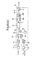
- FIGS. 6A, 6B are detailed circuit block diagrams of synchronous rectifier 14 shown in FIG. 5, FIGS. 6A and 6B illustrating a digital and an analogue types of synchronous rectifiers, respectively.
- a digital type of synchronous rectifier 14A is provided with a wave shaper 22 for forming a rectangular wave signal 23 from the signal sin( ⁇ ot + ⁇ ), a differentiator 24 for producing a pulse signal Pr by differentiating in time an output signal 21 of wave shaper 12 at a time corresponding to rising up of each output rectangular signal 21 as shown in FIG. 6C, another differentiator 26 for producing a pulse signal Pr' by differentiating in time output signal 23 of wave shaper 22 at a time corresponding to rising up of each signal 23 as shown in FIG. 6C, and a flip flop circuit 28 which is set by the pulse Pr and reset by the pulse Pr'.
- the synchronous rectifier 14A is further provided with an AND gate 32 which allows clock pulses Cp from a pulse generator 30 to pass when flip flop 28 is set, a counter 34 for counting the number of the clock pulses supplied from AND gate 32, and a converter 36 for producing a signal V ⁇ sin ⁇ from the values of counter 34 and speed instruction signal V, the value of counter 34 corresponding to the phase difference 9 between the reference signal sin ⁇ ot and a phase modulated signal sin( ⁇ ot + e ) by resolver 2, and converter 36 including a reference memory table 36A for referring to the values 0 and converting it to sine and a digital to analogue converter 36B.
- a multiplier 35 for multiplying the speed instruction signal V and the signal sine is also provided.
- FIG. 6B illustrates an analogue type of synchronous rectifier 14.
- reference numeral 38 is a wave shaper which output signal is logically inverted in a inverter 45 and applied to a switch 44 in analogue switch unit 40. Another output signal of wave shaper 38 is applied to a switch 42 in analogie switch unit 40.
- Switch 42 allows signal V ⁇ sin( ⁇ ot + 0) to pass to a low pass filter 48 which forms a signal V'sine .
- Switch 44 allows inverted signal 47 of V ⁇ sin( ⁇ ot + 6 ), which is formed by an analogue invertor unit 41 having an operational amplifier 46, an input resistance 46A and an feed back resistance 46B, to pass to low pass filter 48.
- reference numeral 16A is an operational amplifier having its gain Gi.
- Reference numerals 16B, 16C and 16D are electric registances.
- Reference numeral 16E is a capacitor.
- the signal V ⁇ sin ⁇ and current feedback signal I fb are supplied to current control loop unit 16 which produces the control signal I*sin ⁇ applied to semiconductor type of drive unit 18.
- the signal I*sin ⁇ is modified to multi phase alternative current signals, each phase signal being supplied to power inverting devices corresponding to each armature windings mounted on the stator of motor 6. So, each armature current makes a revolving magnetic field in motor 6.
- each armature current is supplied in accordance with the rotor's rotation angle 8 equal to the direction of magnetic field in the motor, the phase difference between the directions of the magnetic flux ⁇ and each armature current can be held with right angle ⁇ /2.
- FIG. 7B shows a transfer function G(j ⁇ ) having frequency characteristics depending on the values of " ⁇ ".
- the output signal l a sin( ⁇ - ⁇ ) includes a phase lag ⁇ because of large values in rotary angular velocity ⁇ .
- FIG. 7C is a general control block diagram for suggesting a basic technical concept for eliminating the phase lag 0 indicated in FIG. 7B.
- a block 40 suggests a possibility of phase lag elimination by the way that the signal V'sine is operated with ⁇ formed by motor's rotation speed v and a constant k, thereby the phase 0 being advanced by the angle ⁇ .
- block element Gv corresponding to power amplifier in drive unit 18 has, in general, some delay circuit elements, thereby the total phase lag depending on rotary angular velocity ⁇ becoming larger as much.
- Japanese patent publication No 50-77814 discloses a control circuit for a synchronous motor in which the delay of the armature current is compensated by advancing the nominal pattern signal in accordance with the operating speed of the motor. Because the delay of the armature current is caused by the delay of the response of the control circuit, and also by the delay of the field current, the problem arises that the amount of advancement of the phase in the nominal pattern signal cannot be determined only by the operating speed of the synchronous motor.
- the synchronous motor of JP-A-50-77814 has the disadvantage that it is not able to operate accurately at a pre-set power factor.
- DE-A- 2 734 430 discloses a control circuit for a synchronous motor with signal producing means for detecting an angular position, a phase difference detecting circuit, a phase control circuit connected to the output of the phase difference detecting circuit so as to provide a signal to the plane compensation device.
- Another object of the present invention is to provide a compensation device for compensating a phase lag of an armature current generated in the motor drive unit with current control loop.
- a speed control apparatus for a synchronous motor comprising;
- reference numeral 50 is a circuit in response to the phase modulated signal sin( coot + 0 ) of secondary windings 2c of resolver 2 for producing a speed signal "C" with respect to rotational speeds of rotor 7.
- the circuit 50 comprises a wave shaper for forming a rectangular wave from the phase modulated signal sin( (dot + 0 ), a synchronous rectifier, a low pass filter and a differentiator in time.
- FIGURE 11 illustrates a circuit block diagram for producing a speed signal from a phase modulated signal Eo generated on a secondary winding 101 of a two phase resolver 100.
- reference numeral 104 is a band pass filter
- numeral 106 is a wave shaper
- numerals 108 and 110 are synchronous rectifiers (or phase discriminators)
- numerals 112 and 114 are low pass filters
- numeral 116 is a switching circuit
- numeral 118 is a differentiator in time.
- a signal SQW(dot + e ) designates a signal from wave shaper 106 to be a square wave (rectangular wave) where mo is an angular velocity supplied from a reference signal generator 102 which produces signals SQW1, and SQW2 for using as rectification reference signals to synchronous rectifiers 108 and 110, respectively.
- Reference numeral 52 is a phase compensation circuit located between wave shaper 12 and synchronous rectifier 14, the phase compensation circuit being operated by the speed signal "c", the output of wave shaper 12 being defined as rectangular wave signal "b".
- Reference signal generator 4 produces a signal "a" which is advancing by 7f /2 in its phase angles compared with the reference signal sin ⁇ ot.
- FIGURE 9 illustrates a detailed circuit block diagrams of phase compensation circuit 52 shown in FIG. 8, wherein reference numeral 54 is a integrator which integrates in time the rectangular wave signal "b" (referred to on the time chart (2) in FIG. 10) supplied from wave shaper 12, reference numeral 56 is a comparator for logically comparing the speed signal "c" with signal 54S given from integrator 54, both of the signals “c” and 54S being referred to on the time chart (3) in FIG. 10, and reference numeral 58 designates a logic operation circuit for instance, d-type flip flop for producing a signal "d” referred to on the time chart (7) in FIG. 10, which phase angles are advanced by " 0 " from signal "b". Comparators 56 and 57 produces signals 56S and 57S, respectively. More detailed process of logical operation will be seen in the following description of the time charts (4), (5), (6) and (7) in FIG. 10.
- FIGURE 10 is a group of time charts (1) to (7), each showing signal waves in the phase compensation circuit 52.
- the first time chart (1) shows the reference signal sin( ⁇ ot + ⁇ /2) supplied from reference signal generator 4.
- the second time chart (2) shows the rectangular signal "b" corresponding to the reference signal sin( ⁇ ot + ⁇ /2).
- the third time chart (3) shows the signal "c" with a straight line, the signal 54S with a triangular wave of real line, and the signal 55S with a triangle wave of broken line, respectively, the signal 54S (55S) with a triangle wave being formed as the result that the rectangular wave signal "b" is integrated in time.
- the fifth time chart (5) shows the signal 56S.
- the speed signal "c" equals to "Cl” as shown in the time chart (3)
- the logical value of the signal 56S becomes high (H) when the signal 54S is larger than the speed signal Cl.
- the sixth time chart (6) shows the signal 57S under the condition that the speed signal "c" equals to Cl.
- the logical value of the signal 57S becomes high when the signal 55S is larger than the speed signal Cl.
- the rising up time of signal 55S on the time chart (5) has a phase lead by ⁇ compared with the rising up time of signal 56S on the time chart (4), and that the rising up time of signal 57S on the time chart (6) has also a phase progression by compared with the getting down time of signal 56S on the time chart (4).
- the seventh time chart (7) shows the signal “d" which is an output signal of the phase compensation circuit 52 in FIG. 9, the signal “d” being defined as a signal with its logical value of high (H) only during the time intervals between the rising up time of signal 56S and that of signal 57S.
- circuit 50 when motor 6 rotates at the rotation speed and a phase lag ⁇ is generated in the drive unit, circuit 50 produces a speed signal "C” corresponding to the speed and applies the signal “C” to phase compensation circuit 52.
- Phase compensation circuit 52 in turn produces from the signal “b” the rectangular signal “d” corresponding to a phase modulated signal sin( coot + 0 ), since the circuit 52 functions to advance the signal "b” by the phase angle ⁇ in response to the speed signal "C".
- the amount ⁇ of phase compensation is proportional to the values of angular velocity m of synchronous motor 6 as shown in FIG. 7B.
- speed signal C is produced by circuit 50 connected with the secondary windings 2C of resolver 2
- a tachometer generator can be used instead of circuit 50.
- FIG. 8 discloses a control system for synchronous motor 6, the present invention is also applicable to speed control system for induction motor by frequency control of the primary windings, particularly for induction motors using the vector operation method.
- the phase difference between an armature current and a revolving magnetic field is under the influence of frequency characteristics of power drive unit including current control loop. Accordingly, the phase difference can be cancelled by using the phase compensation method disclosed in the present invention. It is possible for a person skilled in the art to adapt the circuits disclosed in FIG. 8 and 9 to a microprocessor system.
Landscapes
- Engineering & Computer Science (AREA)
- Power Engineering (AREA)
- Control Of Ac Motors In General (AREA)
- Control Of Motors That Do Not Use Commutators (AREA)
Description
- The present invention relates to a speed control apparatus for an electric motor of the type utilizing alternating current in the armature, more specifically to an variable speed control apparatus for a synchronous motor of the type having a revolving magnetic field.
- The synchronous motor of the type having a rotary magnetic field is provided with an armature defining a stator, and field poles defining a rotor. Multi-phase alternating current flowing in the stator windings of the motor generate revolving magnetic fields which cause the rotor to synchronously rotate by magnetic pulling forces acting on it. It is helpful for easily understanding of the invention to explain here the relationships of torques to be generated between a direct current (D.C) motor and a synchronous motor, prior to the description of the conventional speed control apparatus for the synchronous motor.
- Figure 1 A illustrates a sectional view on the rotation axis of a D.C motor, wherein FM are field poles, AM is an armature, AW are armature windings and, DCV is a direct current voltage source. FIG 1B illustrates Fleming's left hand law concerning armature current (la ), field or magnetic flux ( Φ ) and torque (T) to be generated on the D.C motor shown in FIG. 1 A. As shown in FIGS. 1 A and 1B, a rectifier RC switches armature current la so that it always flows in a direction perpendicular to that of magnetic flux In the case, the torque T to be generated is as follows;

- The equation (1) shows that torque T is in proportion to armature current la under the condition that the magnitude of magnetic flux Φ is kept to be constant.
- FIG. 2 illustrates a sectional view on the rotation axis of a synchronous motor provided with rotary field magnetic poles PM, wherein "SW" designates stator windings and "Is" designates current vector flowing in the stator windings "SW". In order to apply the equation (1) to a synchronous motor provided with rotary field magnetic poles as shown in FIG. 2, it is necessary to correspond the magnetic flux Φ to the magnetic flux vector Φs of field poles PM, and further correspond armature current ia to the current vector is of the stator windings SW. Accordingly, the torque T to be generated in the synchronous motor is given in the following equation (2);

- FIG. 3 illustrates an electric circuit equivalent to the synchronous motor shown in FIG. 2. In the figure, Ra designates an electric registance of the stator (armature) windings, and Xs designates a reactance equivalent to the reaction and the leakage magnetic flux on the stator windings. Further, V is voltage source, and y is the phase difference between the armature current is and the electro motive force Eo induced on the stator windings by armature current.
- Therefore, when the phase difference y is zero, that is, the electro motive force Eo is the same with the armature current Is in the phases, the equation (2) becomes as followings;

- The equation (3) shows the possibility that the synchronous motor can be driven by the same fashions in torque generation with D.C motor.
- In other words, the equation (3) indicates that it is necessary for efficiently driving of the synchronous motor to control the armature current Is flowing in the stator windings so as to make the revolving field magnetic flux Φs to be always in right angle with the armature current Is.
- Furthermore, the armature current Is is defined as a function of first order lag to the rotary angular velocity ω of the synchronous motor, which includes a time constant Ta formed with electric registance Ra and inductance La of the stator windings. Accordingly, it results in that the phase lag of the armature current is produced, as the rotation speed of the synchronous motor becomes high.
- It is a conventional way to adopt a current control loop in the drive unit of the synchronous motor for making the phase lag smaller.
- FIG. 4 illustrates a control block diagram corresponding to the drive unit of the motor. In the figure, Gv designates a gain of a current amplifier in the unit, and Gi designates a current feedback gain in the unit.
- In FIG. 4, the transfer function G(s) of the unit is defined as follows;

- Furthermore, open loop gain Go(s) is defined as follows;


- FIG. 5 illustrates a conventional type of control circuit block diagrams for drive control of a synchronous motor.
- In the figure,
reference numeral 2 designates a two phase resolver producing a phase modulated signal with respect to arotary angle 0 of arotor 7 mounted on asynchronous motor 6, andreference numerals resolver 2, each being COS windings and SIN windings to which sinusoidal wave signals cos ωot and sin ωot are applied from areference signal generator 4, respectively.Reference numeral 2c is a secondary winding mounted on a rotor ofresolver 6, the rotor being fixed onrotor 7 ofmotor 6. A signal Sin( ωot + θ) is produced onsecondary windings 2c, as electromotive force generated betweenprimary windings secondary windings 2c. -
Reference numeral 8 is a multiplier for multiplying the output signal sin( ωot + e) and an output signal V of avelocity instruction unit 10.Reference numeral 12 designates a wave shaper for shaping an output signal sin(ωot) to a rectangular pulse trains. -
Reference numeral 14 designates a synchronous rectifier circuit (or phase descriminating circuit) for synchronously rectifying an output signal V'sin( ωot + θ) ofmultiplier 8 with the rectangular wave signal fromwave shaper 12.Reference numeral 16 is a current control loop for producing an control signal I*sine applied to a knownpower drive unit 18 formed with semiconductor devices. Thecurrent control loop 16 receives the signal V'sine and a current feed back signal lfb which is produced at a detectingunit 17 detecting a current actually flowing in the armature ofmotor 6.Reference numeral 20 designates an alternating power source. - FIGS. 6A, 6B are detailed circuit block diagrams of
synchronous rectifier 14 shown in FIG. 5, FIGS. 6A and 6B illustrating a digital and an analogue types of synchronous rectifiers, respectively. - As shown in FIG. 6A, a digital type of
synchronous rectifier 14A is provided with awave shaper 22 for forming arectangular wave signal 23 from the signal sin( ωot + θ), adifferentiator 24 for producing a pulse signal Pr by differentiating in time anoutput signal 21 ofwave shaper 12 at a time corresponding to rising up of each outputrectangular signal 21 as shown in FIG. 6C, anotherdifferentiator 26 for producing a pulse signal Pr' by differentiating intime output signal 23 ofwave shaper 22 at a time corresponding to rising up of eachsignal 23 as shown in FIG. 6C, and aflip flop circuit 28 which is set by the pulse Pr and reset by the pulse Pr'. Thesynchronous rectifier 14A is further provided with anAND gate 32 which allows clock pulses Cp from apulse generator 30 to pass whenflip flop 28 is set, acounter 34 for counting the number of the clock pulses supplied fromAND gate 32, and aconverter 36 for producing a signal V·sinθ from the values ofcounter 34 and speed instruction signal V, the value ofcounter 34 corresponding to thephase difference 9 between the reference signal sin ωot and a phase modulated signal sin( ωot + e ) byresolver 2, andconverter 36 including a reference memory table 36A for referring to thevalues 0 and converting it to sine and a digital toanalogue converter 36B. Amultiplier 35 for multiplying the speed instruction signal V and the signal sine is also provided. - On the other hand, FIG. 6B illustrates an analogue type of
synchronous rectifier 14. In the figure,reference numeral 38 is a wave shaper which output signal is logically inverted in ainverter 45 and applied to a switch 44 inanalogue switch unit 40. Another output signal ofwave shaper 38 is applied to aswitch 42 inanalogie switch unit 40.Switch 42 allows signal V·sin( ωot + 0) to pass to alow pass filter 48 which forms a signal V'sine . Switch 44 allows invertedsignal 47 of V·sin( ωot +6 ), which is formed by ananalogue invertor unit 41 having anoperational amplifier 46, aninput resistance 46A and anfeed back resistance 46B, to pass tolow pass filter 48. FIG. 7A illustrates circuit diagrams ofcurrent control loop 16 shown in FIG. 5. In the figure,reference numeral 16A is an operational amplifier having its gain Gi.Reference numerals Reference numeral 16E is a capacitor. - Hereinafter, the functions and operations of circuit block diagrams shown in FIG. 5 will be explained.
- In the figure, when
rotor 7 rotatably mounted onsynchronous motor 6 rotates at its angular velocity ωand its rotary angle becomes at anangle 0 as shown in the figure, secondary windings 2C ofresolver 2 produces a phase modulated signal sin( ωot+θ).Multiplier 8 multiplies speed instruction signal V and the phase modulated signal sin(ωot+ θ), thereby producing the signal V·sin( ωot+ θ).Synchronous rectifier 14 synchronously rectifiers the signal V·sin( ωot + 0) by a rectangular wave signal given fromwave shaper 12, and produces the signal V·sin 0 corresponding to the angular position ofrotor 7. - Further, the signal V·sinθ and current feedback signal Ifb are supplied to current
control loop unit 16 which produces the control signal I*sinθ applied to semiconductor type ofdrive unit 18. In theunit 18, the signal I*sinθ is modified to multi phase alternative current signals, each phase signal being supplied to power inverting devices corresponding to each armature windings mounted on the stator ofmotor 6. So, each armature current makes a revolving magnetic field inmotor 6. As mentioned above, since each armature current is supplied in accordance with the rotor'srotation angle 8 equal to the direction of magnetic field in the motor, the phase difference between the directions of the magnetic flux Φ and each armature current can be held with right angle π/2. - However, as the rotation speed becomes high and the angular velocity ω becomes large values, the equation (5) does not hold. FIG. 7B shows a transfer function G(j ω) having frequency characteristics depending on the values of "ω".
- In the figure, the output signal lasin( θ - φ ) includes a phase lag φ because of large values in rotary angular velocity ω . In the case, φ is defined as the phase angle of the transfer function G(jω), as follows; φ = arg·G(jω)
- FIG. 7C is a general control block diagram for suggesting a basic technical concept for eliminating the phase lag 0 indicated in FIG. 7B. In the figure 7C, a
block 40 suggests a possibility of phase lag elimination by the way that the signal V'sine is operated with φ formed by motor's rotation speed v and a constant k, thereby thephase 0 being advanced by the angle φ. - Furthermore, as shown in FIG. 4 and FIG. 5, block element Gv corresponding to power amplifier in
drive unit 18 has, in general, some delay circuit elements, thereby the total phase lag depending on rotary angular velocity ω becoming larger as much. - Therefore, in the conventional speed control apparatus for the synchronous motor shown in FIG. 5, a desired controlability cannot be obtained as the motor rotates at high speed because of generating phase differences between revolving magnetic field and armature current (la).
- Japanese patent publication No 50-77814 discloses a control circuit for a synchronous motor in which the delay of the armature current is compensated by advancing the nominal pattern signal in accordance with the operating speed of the motor. Because the delay of the armature current is caused by the delay of the response of the control circuit, and also by the delay of the field current, the problem arises that the amount of advancement of the phase in the nominal pattern signal cannot be determined only by the operating speed of the synchronous motor.
- In consequence, the synchronous motor of JP-A-50-77814 has the disadvantage that it is not able to operate accurately at a pre-set power factor.
- DE-A- 2 734 430 discloses a control circuit for a synchronous motor with signal producing means for detecting an angular position, a phase difference detecting circuit, a phase control circuit connected to the output of the phase difference detecting circuit so as to provide a signal to the plane compensation device.
- There is no teaching in this document of a rotational Speed signal producing means responsive to an angular portion to produce a signal corresponding to the Speed of the motor, which influences the phase compensation circuit.
- Accordingly, it is a primary object of the present invention to provide a control apparatus for a synchronous motor in which revolving magnetic field with magnetic flux Φ and an armature current la are always controlled so as to be at right angles to each other, whereby a desired control can be obtained even at the high rotational speed range of the motor. Another object of the present invention is to provide a compensation device for compensating a phase lag of an armature current generated in the motor drive unit with current control loop.
- According to the present invention there is provided a speed control apparatus for a synchronous motor comprising;
- means for designating a rotational speed of the motor;
- means for producing an angular position signal with respect to an angular position of a revolving magnetic field corresponding to that of a rotor on the motor; and
- means for producing an armature current command signal in accordance with a speed instruction supplied from said speed designating means and said angular position signal supplied from said angular position signal producing means;
characterised by rotational speed signal producing means responsive to said angular position signal for producing a speed signal corresponding to the speed of said motor; - phase compensation means responsive to said speed signal for advancing a phase of said armature current commend signal with respect to the angular position of said rotor of the motor; and
- means for producing a desired armature current on armature windings of the motor including a current control loop circuit responsive to said phase-advanced armature current command signal for outputting said desired armature current.
- In the accompanying drawings;
- Figure 1 A is a sectional view on the axis of a direct current motor for explaining torque generation thereon;
- Figure 1 B illustrates relationships of directions among an armature current, a magnetic field and a torque;
- Figure 2 is a sectional view on the axis of a synchronous motor of the type having a revolving magnetic field;
- FIGURE 3 is a equivalent circuitry of the motor shown in FIG. 2;
- FIGURE 4 is a general block diagram of transfer functions corresponding to a speed control system for a synchronous motor;
- FIGURE 5 illustrates a block diagram of a conventional control circuitry for a synchronous motor;
- FIGURE 6A illustrates a digital type of synchronous rectifier circuitry;
- FIGURE 6B illustrates an analogue type of synchronous rectifier circuitry;
- FIGURE 6C is a time chart of signals in FIG. 6A;
- FIGURE 7A illustrates a circuitry of the current control loop;
- FIGURE 7B is a block diagram of the transfer function corresponding to a power drive unit including a current control loop and armature windings for suggesting a presence of phase lags therein;
- FIGURE 7C is a block diagram for suggesting a phase compensation by the present invention;
- FIGURE 8 is a circuit block diagram of a speed control apparatus due to the present invention;
- FIGURE 9 is a detailed circuit block diagram of a phase compensation circuit shown in FIG. 8;
- FIGURE 10 illustrates time charts of each signal shown in FIG. 9; and
- FIGURE 11 illustrates a circuit block diagram for producing a speed signal from a phase modulated signal Eo generated on a secondary winding of a two phase resolver.

- In FIG 8, reference numerals for elements corresponding to those shown in FIGURE 5 are same numbers.
- Referring to the figure 8,
reference numeral 50 is a circuit in response to the phase modulated signal sin( coot + 0 ) ofsecondary windings 2c ofresolver 2 for producing a speed signal "C" with respect to rotational speeds ofrotor 7. As shown in figure 11, thecircuit 50 comprises a wave shaper for forming a rectangular wave from the phase modulated signal sin( (dot + 0 ), a synchronous rectifier, a low pass filter and a differentiator in time. - FIGURE 11 illustrates a circuit block diagram for producing a speed signalfrom a phase modulated signal Eo generated on a secondary winding 101 of a two
phase resolver 100. In the figure,reference numeral 104 is a band pass filter, numeral 106 is a wave shaper,numerals numerals - A signal SQW(dot + e ) designates a signal from
wave shaper 106 to be a square wave (rectangular wave) where mo is an angular velocity supplied from areference signal generator 102 which produces signals SQW1, and SQW2 for using as rectification reference signals tosynchronous rectifiers - Signal E1 (=sinωot) and E2 (= cosωot) generated in
reference signal generator 102 are used as exciting signals supplied toprimary windings resolver 100. More detailed circuit diagrams and its operations can be understood by referring to Japanese Patent publication numbers; 57-187659 and 57-187660 or U.S. serial number 363525. -
Reference numeral 52 is a phase compensation circuit located betweenwave shaper 12 andsynchronous rectifier 14, the phase compensation circuit being operated by the speed signal "c", the output ofwave shaper 12 being defined as rectangular wave signal "b". -
Reference signal generator 4 produces a signal "a" which is advancing by 7f /2 in its phase angles compared with the reference signal sin ω ot. - FIGURE 9 illustrates a detailed circuit block diagrams of
phase compensation circuit 52 shown in FIG. 8, whereinreference numeral 54 is a integrator which integrates in time the rectangular wave signal "b" (referred to on the time chart (2) in FIG. 10) supplied fromwave shaper 12,reference numeral 56 is a comparator for logically comparing the speed signal "c" withsignal 54S given fromintegrator 54, both of the signals "c" and 54S being referred to on the time chart (3) in FIG. 10, andreference numeral 58 designates a logic operation circuit for instance, d-type flip flop for producing a signal "d" referred to on the time chart (7) in FIG. 10, which phase angles are advanced by "0" from signal "b".Comparators signals - FIGURE 10 is a group of time charts (1) to (7), each showing signal waves in the
phase compensation circuit 52. - Referring to FIGURE 10, the first time chart (1) shows the reference signal sin( ωot + π /2) supplied from
reference signal generator 4. - The second time chart (2) shows the rectangular signal "b" corresponding to the reference signal sin( ωot + π /2).
- The third time chart (3) shows the signal "c" with a straight line, the
signal 54S with a triangular wave of real line, and thesignal 55S with a triangle wave of broken line, respectively, thesignal 54S (55S) with a triangle wave being formed as the result that the rectangular wave signal "b" is integrated in time. - The forth time chart (4) shows the
signal 56S when the speed signal "c"=0, that is, when thesignal 54S is larger than the speed signal "c"(=0), the logical value of thesignal 56S becomes high. Also, it should be noted that thesignal 56S under the speed signal C(=0) has a delay of phase difference π/2 compared with the signal "b". - The fifth time chart (5) shows the
signal 56S. In case that the speed signal "c" equals to "Cl" as shown in the time chart (3), the logical value of thesignal 56S becomes high (H) when thesignal 54S is larger than the speed signal Cl. - The sixth time chart (6) shows the
signal 57S under the condition that the speed signal "c" equals to Cl. In the case, the logical value of thesignal 57S becomes high when thesignal 55S is larger than the speed signal Cl. Also, it should be noted that the rising up time ofsignal 55S on the time chart (5) has a phase lead by φ compared with the rising up time ofsignal 56S on the time chart (4), and that the rising up time ofsignal 57S on the time chart (6) has also a phase progression by compared with the getting down time ofsignal 56S on the time chart (4). - The seventh time chart (7) shows the signal "d" which is an output signal of the
phase compensation circuit 52 in FIG. 9, the signal "d" being defined as a signal with its logical value of high (H) only during the time intervals between the rising up time ofsignal 56S and that ofsignal 57S. - Functions and operations of the system illustrated in figure 8 will be explained as follows.
- In the figure 8, when
motor 6 rotates at the rotation speedand a phase lag φ is generated in the drive unit,
circuit 50 produces a speed signal "C" corresponding to the speed and applies the signal "C" to phasecompensation circuit 52.Phase compensation circuit 52 in turn produces from the signal "b" the rectangular signal "d" corresponding to a phase modulated signal sin( coot + 0 ), since thecircuit 52 functions to advance the signal "b" by the phase angle φ in response to the speed signal "C". - Then, signal V·sin(ω ot +6 ) given from
multiplier 8 is synchronously rectified by the signal "d" atsynchronous rectifier 14, thereby a signal sin( 0 + φ ) being produced. Accordingly, since the input signal to currentcontrol loop circuit 16 is in advance progressed by phase angle φ corresponding to the phase lag in the current control loop, the output signal ofcurrent control loop 16 results in I*sin e, that is, phase lags generated oncurrent control loop 16 can be cancelled. - In the case mentioned above, the amount φ of phase compensation is proportional to the values of angular velocity m of
synchronous motor 6 as shown in FIG. 7B. - In the strict meaning, however, an actual current feedback loop has an element with first order lag, and the amount φ of the phase compensation holds the following equation;

- In case very strict accuracy for the relationships between 0 and ω is required, it is possible to read out more accurate
digital data 0 corresponding to each measured angular velocity ω from a memory storing the relationships between 0 and ω , that is, the equation (7). - Though in FIG. 8 speed signal C is produced by
circuit 50 connected with the secondary windings 2C ofresolver 2, a tachometer generator can be used instead ofcircuit 50. Though FIG. 8 discloses a control system forsynchronous motor 6, the present invention is also applicable to speed control system for induction motor by frequency control of the primary windings, particularly for induction motors using the vector operation method. - In the vector operation method, as the induction motor rotates at very high speed, the phase difference between an armature current and a revolving magnetic field is under the influence of frequency characteristics of power drive unit including current control loop. Accordingly, the phase difference can be cancelled by using the phase compensation method disclosed in the present invention. It is possible for a person skilled in the art to adapt the circuits disclosed in FIG. 8 and 9 to a microprocessor system.
- As mentioned before, it is an advantage of the present invention to be capable of driving a synchronous motor efficiently, because of always keeping the phase angles between the rotary magnetic field and the armature current of the motor to be 7T /2 in a broad range of motor's rotation. It is another advantage of the invention to drive the synchronous motor without heat generation under high speed rotation. It is still another advantage of the present invention to drive the synchronous motor with quick response to the changing of speed instruction.
Claims (10)
characterised by rotational speed signal producing means (50) responsive to said angular position signal for producing a speed signal corresponding to the speed of said motor;
Applications Claiming Priority (2)
| Application Number | Priority Date | Filing Date | Title |
|---|---|---|---|
| JP59115340A JPS60261386A (en) | 1984-06-05 | 1984-06-05 | Speed controller of ac motor |
| JP115340/84 | 1984-06-05 |
Publications (2)
| Publication Number | Publication Date |
|---|---|
| EP0170368A1 EP0170368A1 (en) | 1986-02-05 |
| EP0170368B1 true EP0170368B1 (en) | 1991-05-02 |
Family
ID=14660116
Family Applications (1)
| Application Number | Title | Priority Date | Filing Date |
|---|---|---|---|
| EP85303951A Expired - Lifetime EP0170368B1 (en) | 1984-06-05 | 1985-06-04 | Speed control apparatus for a synchronous motor |
Country Status (5)
| Country | Link |
|---|---|
| US (1) | US4734633A (en) |
| EP (1) | EP0170368B1 (en) |
| JP (1) | JPS60261386A (en) |
| KR (1) | KR900007109B1 (en) |
| DE (1) | DE3582704D1 (en) |
Families Citing this family (18)
| Publication number | Priority date | Publication date | Assignee | Title |
|---|---|---|---|---|
| IT1204384B (en) * | 1986-06-06 | 1989-03-01 | Elge App Elettron | PROCEDURE AND EQUIPMENT SUITABLE FOR DRIVING SYNCHRONOUS MOTORS, IN PARTICULAR SERVOMOTORS |
| JP2674024B2 (en) * | 1987-06-25 | 1997-11-05 | トヨタ自動車株式会社 | Servo controller |
| JP2825962B2 (en) * | 1990-10-30 | 1998-11-18 | ジューキ株式会社 | AC motor drive |
| JPH05336789A (en) * | 1992-06-01 | 1993-12-17 | Fanuc Ltd | Controlling system of motor |
| US5650708A (en) * | 1992-12-08 | 1997-07-22 | Nippondenso Co., Ltd. | Inverter control apparatus using a two-phase modulation method |
| JPH0923700A (en) * | 1995-06-30 | 1997-01-21 | Fanuc Ltd | Servo motor current control |
| US5818192A (en) * | 1995-08-04 | 1998-10-06 | The Boeing Company | Starting of synchronous machine without rotor position of speed measurement |
| JP4737858B2 (en) * | 2001-03-27 | 2011-08-03 | 東芝エレベータ株式会社 | Control device for permanent magnet motor |
| JP3501370B2 (en) * | 2001-09-04 | 2004-03-02 | 株式会社デンソー | Control method and control device for synchronous motor |
| DE10223869A1 (en) * | 2002-05-29 | 2003-12-11 | Leybold Vakuum Gmbh | Two-shaft vacuum pump |
| US9118529B2 (en) * | 2006-06-20 | 2015-08-25 | Qualcomm Incorporated | Discovery of neighbor cells |
| US8612502B2 (en) * | 2007-03-21 | 2013-12-17 | Qualcomm Incorporated | Simplified equalization for correlated channels in OFDMA |
| GB2489434A (en) * | 2011-03-25 | 2012-10-03 | Technelec Ltd | Controlling an electrical machine with an observer |
| JP5947075B2 (en) * | 2012-03-23 | 2016-07-06 | Dmg森精機株式会社 | Synchronous motor control device and synchronous motor control method |
| CN103967794B (en) * | 2013-02-05 | 2016-01-20 | 广东美的制冷设备有限公司 | A kind of method for compensating vibration of single-rotor compressor and controller |
| RU2609673C2 (en) * | 2015-04-06 | 2017-02-02 | Акционерное общество "Научно-производственный центр "Полюс" | Method of controlling electric motor rpm |
| KR102575175B1 (en) * | 2018-07-27 | 2023-09-05 | 현대자동차 주식회사 | Apparatus and method of retificating resolver output signal |
| US20210140798A1 (en) * | 2019-11-12 | 2021-05-13 | Hamilton Sundstrand Corporation | Determining a rotational direction of a resolver |
Family Cites Families (15)
| Publication number | Priority date | Publication date | Assignee | Title |
|---|---|---|---|---|
| GB1046983A (en) * | 1964-03-23 | 1966-10-26 | Sequential Electronic Systems | Improvements in or relating to control systems |
| JPS5850119B2 (en) * | 1976-07-30 | 1983-11-08 | 株式会社日立製作所 | Control device for commutatorless motor |
| JPS5358610A (en) * | 1976-11-06 | 1978-05-26 | Nippon Telegr & Teleph Corp <Ntt> | Phase-lead compensaion for dc brushless motor |
| US4357569A (en) * | 1977-08-17 | 1982-11-02 | Kabushiki Kaisha Yaskawa Denki Seisakusho | Control device for a synchronous motor |
| US4358722A (en) * | 1977-08-17 | 1982-11-09 | Kabushiki Kaisha Yaskawa Denki Seisakusho | Speed detector using resolver |
| JPS5947956B2 (en) * | 1977-12-05 | 1984-11-22 | 株式会社日立製作所 | Control method of commutatorless motor |
| JPS5953795B2 (en) * | 1978-02-03 | 1984-12-26 | 株式会社日立製作所 | Thyristor motor control device |
| JPS54113815A (en) * | 1978-02-27 | 1979-09-05 | Toshiba Corp | Controlling ac motor |
| SU864476A1 (en) * | 1979-03-15 | 1981-09-15 | Предприятие П/Я М-5774 | Electric drive |
| JPS576584A (en) * | 1980-06-12 | 1982-01-13 | Toshiba Mach Co Ltd | Controller for drive of synchronous motor |
| US4447771A (en) * | 1981-08-31 | 1984-05-08 | Kollmorgen Technologies Corporation | Control system for synchronous brushless motors |
| JPS58123395A (en) * | 1982-01-18 | 1983-07-22 | Fanuc Ltd | Control system for synchronous motor |
| JPS58130792A (en) * | 1982-01-28 | 1983-08-04 | Fanuc Ltd | Drive device for synchronous motor |
| IT1151308B (en) * | 1982-03-23 | 1986-12-17 | Sp El Srl | CIRCUIT FOR THE GENERATION OF MULTI-PHASE SIGNALS, VARIABLE IN AMPLITUDE AND PHASE, NECESSARY AS A CURRENT OR VOLTAGE REFERENCE FOR DRIVING SYNCHRONOUS MOTORS |
| JPS59123482A (en) * | 1982-12-29 | 1984-07-17 | Fanuc Ltd | Control system for synchronous motor |
-
1984
- 1984-06-05 JP JP59115340A patent/JPS60261386A/en active Pending
-
1985
- 1985-06-04 DE DE8585303951T patent/DE3582704D1/en not_active Expired - Lifetime
- 1985-06-04 EP EP85303951A patent/EP0170368B1/en not_active Expired - Lifetime
- 1985-06-05 KR KR1019850003947A patent/KR900007109B1/en not_active Expired
- 1985-06-05 US US06/741,585 patent/US4734633A/en not_active Expired - Fee Related
Also Published As
| Publication number | Publication date |
|---|---|
| JPS60261386A (en) | 1985-12-24 |
| US4734633A (en) | 1988-03-29 |
| DE3582704D1 (en) | 1991-06-06 |
| KR900007109B1 (en) | 1990-09-28 |
| KR860000743A (en) | 1986-01-30 |
| EP0170368A1 (en) | 1986-02-05 |
Similar Documents
| Publication | Publication Date | Title |
|---|---|---|
| US4734633A (en) | Speed control apparatus for a synchronous motor | |
| EP0109075B1 (en) | Rotary drive system positioning apparatus by means of resolvers | |
| EP0030462B1 (en) | Induction motor drive apparatus | |
| EP0075023B1 (en) | Method of controlling an ac motor and device thereof | |
| US4358726A (en) | Current type inverter | |
| US4125796A (en) | Control apparatus for use in a synchronous machine | |
| EP0279415A1 (en) | Induction motor control apparatus | |
| US4357569A (en) | Control device for a synchronous motor | |
| DE3123091C2 (en) | ||
| US4484126A (en) | Induction motor controller | |
| EP0067886A1 (en) | Induction motor drive system | |
| US4837493A (en) | System for driving drum | |
| US4259628A (en) | Control device of AC motor | |
| JPS6148350B2 (en) | ||
| EP0077403A1 (en) | Speed detecting device | |
| US3551766A (en) | Regulatable and controllable inverter or frequency changer arrangement for feeding ac motors | |
| EP0133580A1 (en) | Permanent magnet synchronous motor control system | |
| EP0073839B1 (en) | Control device for synchronous motor | |
| KR880001593B1 (en) | Ac motor speed control system | |
| CA1283442C (en) | System for driving drum | |
| RU2074394C1 (en) | Method of measurement of parameters of a c electric machine and device to implement it | |
| JPS6225893A (en) | Synchronous motor control device | |
| JPS6333616A (en) | Resolver digital converter | |
| JPH04261386A (en) | Pole position detecting method for synchronous motor | |
| JPS6295987A (en) | AC motor control device |
Legal Events
| Date | Code | Title | Description |
|---|---|---|---|
| PUAI | Public reference made under article 153(3) epc to a published international application that has entered the european phase |
Free format text: ORIGINAL CODE: 0009012 |
|
| AK | Designated contracting states |
Designated state(s): DE FR GB IT SE |
|
| 17P | Request for examination filed |
Effective date: 19860620 |
|
| 17Q | First examination report despatched |
Effective date: 19871208 |
|
| ITF | It: translation for a ep patent filed | ||
| GRAA | (expected) grant |
Free format text: ORIGINAL CODE: 0009210 |
|
| AK | Designated contracting states |
Kind code of ref document: B1 Designated state(s): DE FR GB IT SE |
|
| RAP1 | Party data changed (applicant data changed or rights of an application transferred) |
Owner name: TOEI DENKI KABUSHIKI KAISHA Owner name: TOSHIBA KIKAI KABUSHIKI KAISHA |
|
| REF | Corresponds to: |
Ref document number: 3582704 Country of ref document: DE Date of ref document: 19910606 |
|
| ET | Fr: translation filed | ||
| PLBE | No opposition filed within time limit |
Free format text: ORIGINAL CODE: 0009261 |
|
| STAA | Information on the status of an ep patent application or granted ep patent |
Free format text: STATUS: NO OPPOSITION FILED WITHIN TIME LIMIT |
|
| 26N | No opposition filed | ||
| PGFP | Annual fee paid to national office [announced via postgrant information from national office to epo] |
Ref country code: GB Payment date: 19930512 Year of fee payment: 9 |
|
| PGFP | Annual fee paid to national office [announced via postgrant information from national office to epo] |
Ref country code: DE Payment date: 19930515 Year of fee payment: 9 |
|
| PGFP | Annual fee paid to national office [announced via postgrant information from national office to epo] |
Ref country code: SE Payment date: 19930519 Year of fee payment: 9 Ref country code: FR Payment date: 19930519 Year of fee payment: 9 |
|
| PG25 | Lapsed in a contracting state [announced via postgrant information from national office to epo] |
Ref country code: GB Effective date: 19940604 |
|
| PG25 | Lapsed in a contracting state [announced via postgrant information from national office to epo] |
Ref country code: SE Effective date: 19940605 |
|
| EUG | Se: european patent has lapsed |
Ref document number: 85303951.9 Effective date: 19950110 |
|
| GBPC | Gb: european patent ceased through non-payment of renewal fee |
Effective date: 19940604 |
|
| PG25 | Lapsed in a contracting state [announced via postgrant information from national office to epo] |
Ref country code: FR Effective date: 19950228 |
|
| PG25 | Lapsed in a contracting state [announced via postgrant information from national office to epo] |
Ref country code: DE Effective date: 19950301 |
|
| EUG | Se: european patent has lapsed |
Ref document number: 85303951.9 |
|
| REG | Reference to a national code |
Ref country code: FR Ref legal event code: ST |