EP0169527B1 - Signal converting method and circuit for television receiver - Google Patents
Signal converting method and circuit for television receiver Download PDFInfo
- Publication number
- EP0169527B1 EP0169527B1 EP85109133A EP85109133A EP0169527B1 EP 0169527 B1 EP0169527 B1 EP 0169527B1 EP 85109133 A EP85109133 A EP 85109133A EP 85109133 A EP85109133 A EP 85109133A EP 0169527 B1 EP0169527 B1 EP 0169527B1
- Authority
- EP
- European Patent Office
- Prior art keywords
- signal
- scanning lines
- field
- line
- adjacent
- Prior art date
- Legal status (The legal status is an assumption and is not a legal conclusion. Google has not performed a legal analysis and makes no representation as to the accuracy of the status listed.)
- Expired - Lifetime
Links
Images


Classifications
-
- H—ELECTRICITY
- H04—ELECTRIC COMMUNICATION TECHNIQUE
- H04N—PICTORIAL COMMUNICATION, e.g. TELEVISION
- H04N7/00—Television systems
- H04N7/01—Conversion of standards, e.g. involving analogue television standards or digital television standards processed at pixel level
- H04N7/0117—Conversion of standards, e.g. involving analogue television standards or digital television standards processed at pixel level involving conversion of the spatial resolution of the incoming video signal
- H04N7/012—Conversion between an interlaced and a progressive signal
Definitions
- the present invention relates to a signal converting method and circuit for a television signal, particularly to a scanning. line converting method for a high resolutional television receiver and a circuit thereof.
- a system for doubling the number of the scanning lines by using line memories has been developped and is known as the 1:1 non-interlaced scanning with line interpolation system.
- the average line interpolation system is described, for example, in Japanese Patent Application Laid-Open No. 79378/83.
- the systems have problems such that line flicker is emphasized rather than diminished or that resolution in the vertical direction is degraded on some video signal patterns.
- the European patent application EP-A-0 018 856 describes a line interpolation of a television signal with improved resolution of the display image, the field rate being doubled from that of a received input television signal.
- the video signal of an adjacent field is used as a component of the line interpolation signal in the still picture, and the interpolation for the motion picture in an average interpolation.
- image data like a television signal of a previous field is used to control scanning line interpolation of image data for two adjacent scanning lines in a current or present field.
- a signal converting circuit is constructed with line memories for storing image data of two adjacent scanning lines of the present field, field memories for storing image data of the previous field, and means for differentiating image data of the two adjacent scanning lines and image data of the previous field and for determining a line interpolation signal of the two adjacent scanning lines in the present field.
- image data in the previous field corresponding to a line, for which the interpolation signal is determined is used. That is, an interpolation coefficient is determined by subtracting an average signal of image data of two adjacent scanning lines in the present field and image data in the previous field corresponding to the position of the line interpolation signal.
- image data having an analog form or a digital form especially, a color television signal is separated into a brightness, or luminance component and a color difference component and the luminance component is subjected to the scanning line interpolation with image data of the previous field and the present field, whereas the color difference component is subjected to the scanning line interpolation with image data of the present field, because the line flicker is based mainly on the luminance component.
- Fig. 1 is a block diagram showing the fundamental concept of the prior art.
- Reference numeral 1 indicates an input terminal; numeral 2 a switch; numerals 3, 4 and 5, line memories of 1H, where H indicates a horizontal period; numeral 6 a switch; numeral 7 an adder; numeral 8 a half attenuator; numeral 9 a switch; numeral 10 an output terminal; numeral 11 a line memory control circuit; and numerals 12, 13 and 14 read/write (R/W) control signals.
- R/W read/write
- the line memories 3, 4 and 5 are designated at A, B and C, they operate at such times, respectively, as are illustrated in Figs. 2A, 2B and 2C.
- the A-line memory 3 is in a write period (W)
- the B- and C-line memories 4 and 5 are in read periods (R).
- the reading from each line memory is conducted twice for the 1H period, as shown in Figs. 2A to 2C because it is executed at a double rate.
- This R/W control is in response to the R/W control signals 12, 13 and 14 provided from the line memory control circuit 11.
- switch 2 is connected for each successive 1H period with the three line memories 3, 4 and 5 so that the signal for each line is stored into each line memory for different write periods.
- the operation is shifted to the read period so that the reading is repeated two times for each 1/2H period.
- the signal as read is supplied to the switch 6 so that the image data of the line memories is provided in response to a switching signal 15 supplied from control circuit 11 at times shown in Figs. 2E and 2F.
- the output signals designated by numerals 16 and 17 from the switch are averaged by the adder 7 and the half attenuator 8, and are supplied to switch 9.
- This switch 9 is switched for each 1/2H period so that the original signal and the line interpolation signal alternately occur at terminal 10, as shown in Fig., 2F. As a result, a signal converted to a double scanning rate is provided.
- terminal 10 By fixing switch 9 at the upper side, terminal 10 provides the signal train of Fig. 2F which is interpolated by the double repetitions of the scanning lines.
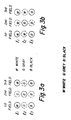
- the scanning line l1 is assumed to be white whereas the scanning lines l2 and l3 are assumed to be black; the brightness of image is also assumed to vary between the scanning lines l1 and l2.
- the scanning line l2 is an average of the scanning lines l1 and l3 so that it takes on a grey hue.
- a similar interpolation is conducted in the second and third fields.
- the White and gray hues are alternately repeated for each field so that line flicker is decreased. This decrease also occurs for scanning line l2.
- This system has an advantage that line flicker is made smaller than the case where scanning lines are not interpolated, because interpolations in this average line interpolation system are made with a neutral hue such as grey. In the average line interpolation system, however, the boundaries are blurred by the grey hue so that vertical resolution becomes worse.
- scanning line l2 of the first field is the same interpolation of the scanning line l1 so that it appears white.
- the scanning line l1 of the second field is the same as the previous scanning line which is not shown, so that it takes on a white hue, whereas the scanning line l3 is caused to take on black hue by repeatedly interpolating the scanning line l2.
- the scanning line l2 of the third field takes on a white hue like the first field. If the white and black hues of scanning line l2 are repeated for each field, 30 Hz line flicker occurs.
- the same line interpolation system emphasizes the line flickers more than a system not using any imterpolation system.
- Reference numeral 21 indicates an interpolating circuit; numeral 22 a switch; numeral 23 a first field memory; numeral 24 a second field memory (F ); numeral 25 a switch; numeral 26 a field memory control circuit; numerals 27 and 28 field memory R/W switching signals; and numeral 29 a field memory output image signal.
- the same elements shown in Fig. 1 are indicated with the same reference numerals.
- the operations of the embodiment of the present invention will be described in the following paragraphs. Referring to Fig. 4, the operations of switch 2, line memories 3, 4 and 5, switch 6, and line memory control circuit 11 are the same as those of the example discussed earlier herein and shown in Fig. 1, so that their descriptions are omitted.
- line memories 3, 4 and 5 execute the operations described above. Only one of the field memories 23 and 24 is selected by switch 22 so that the field memory selected is written with the image of one field.
- the scanning lines are read during a single vertical scanning period two-by-two at double the rate for a subsequent single field.
- Switch 25 is connected with one of the field memories 23 and 24 in the reading operation to send the image data to the interpolating circuit 21.
- the field memories 23 and 24 operate at the times shown in Figs. 5a and 5b in response to the R/W switching signals 27 and 28 output from the field memory control circuit 25.
- the switches 22 and 25 are also switched for each field so that they are always connected with one of the field memories.
- field memories (F1 ) 23 and (F2 ) 24 would require vast memory capacities if they stored all the signals of one field.
- the data of the field memories are used only for judgment, not as interpolated signals, as will be described. Therefore, it is possible in the present invention to reduce the memory capacities of the field memories.
- the objects of the present invention can be achieved even if the number of the total picture elements, that is, the precision of each picture element written into the field memories, are reduced by between one-third and one-fourth.
- the output signals 16 and 17, that is, image data of the present field, are supplied to the interpolating circuit 21, together with the output signal 29 occurring at switch 25, that is, the image data of the preceding field. Relationship of these output signals is illustrated in Fig. 6, where image data of three continuous fields and scanning lines are shown. Referring to Fig. 6, X indicates a scanning line corresponding to image data 16, Y indicates a scanning line corresponding to image data 17 and Z indicates a scanning line corresponding to line information contained in the image data 29.
- the interpolating circuit 21 generates the line interpolation signal by varying a mixing ratio between image data 16 and image data 17 in response to the output signal 29 and provides a luminance signal converted to have high quality, to output terminal 10'.
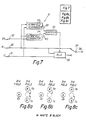
- FIG. 7 shows the construction of the interpolating circuit 21 of Fig. 4.
- Numerals 30, 31 and 32 denote input terminals receiving the output signals 16, 17 and 29, respectively.
- Numerals 33 and 34 designate an intrafield scanning line comparator and an interfield scanning line comparator, respectively.
- Numerals 35, 36, 37 and 38 indicate an encoder, an arithmetic logic circuit (ALU), a switch (S6) and an output terminal connected with the output terminal 10'.
- ALU arithmetic logic circuit
- S6 switch
- a dotted line appearing in the third field indicates the interpolated scanning line which is produced by the interpolating circuit 21.
- intrafield scanning line comparator 33 compares the luminance signals of scanning lines X and Y to provide a correlation coefficient ⁇ as an output signal 39.
- interfield scanning line comparator 34 compares the luminance signals of the scanning lines X and Z to provide a correlation coefficient ⁇ as an output signal 40.
- Encoder 35 produces an arithmetic switching signal in accordance with the magnitude of the correlation coefficients ⁇ and ⁇ to send the switching signal to ALU 36. In response to the arithmetic switching signal, ALU 36 switches and averages scanning lines X and Y.
- the interpolated scanning line signal is applied to the switch 37, which is alternately switched between the original scanning line so that the interpolated scanning line signal is converted into a signal having twice as many scanning lines and is supplied to the terminal 38. This converted signal is supplied as a final output to the terminal 10'.
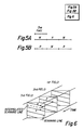
- Figs. 8a, 8b and 8c show how to interpolate between arbitrary picture elements of scanning lines X, Y and Z of Fig. 6.
- the color difference signal will be described in the following.
- the averaging method of the prior art can achieve the interpolations while considering that the visual characteristics of an observer are inferior to that of the luminance signal. Therefore, it is possible to omit the field memory for the color difference signal.
- the color difference signal is input to the input terminal 1, as shown in Fig. 4, scanning line interpolations are conducted by the line memories, as has been described herein, so that a color difference signal having twice the number of scanning lines occurs at terminal 10.
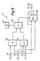
- FIG. 9 illustrates a block diagram of the interpolating circuit 21 shown in Fig. 4.
- Numerals 30, 31, 32, 37 and 38 indicate the same parts as shown in Fig. 7.
- circuit 105 provides an output signal ⁇ , that is, (X-Y).
- circuit 106 When the scanning lines X, Y and Z are applied to a circuit 106, which includes a subtracting circuit and an averaging circuit, circuit 106 provides an output signal , that is, (X+Y)/2 - Z. These signals ⁇ and ⁇ are supplied to circuit 107 for providing an interpolation coefficient ⁇ .
- Interpolation coefficient circuit 107 comprising a dividing circuit, provides interpolation coefficient ⁇ , equal to (1/2 + ⁇ / ⁇ ).
- the fraction ⁇ / ⁇ expresses nomalization of the output signal of the interfield comparision by output signals ⁇ of the intrafield comparison.
- interpolation coefficient ⁇ approaches 1, which shows that there is large correlation between the scanning line Z, and the scanning line Y.
- ⁇ / ⁇ is smaller, that is, near to (-1/2)
- the interpolation coefficient approaches zero, which indicates that the correlation between the scanning line X and the scanning line Z is small.
- interpolation coefficient approaches 1/2, which indicates that the correlation between the scanning line X and the scanning line Y is large.
- the interpolation coefficient is set to 1/2. Namely, in the case that
- the value of adding the noise threshold to scanning line Z is smaller than the smaller one of scanning lines X and scanning line Y; that is, this indicates that it is impossible to correlate the image data of the present field and the line information of the preceding field. Also, the same situation may happen in a case where an object has a luminence signal extremely different from the luminance signal of its surrounding. Therefore, the interpolation coefficient is set to 1/2, where the resolution may become a little inferior. In the case of ii), the value of subtracting the noise threshold ⁇ from scanning line Z is larger than the larger one of the scanning lines X and Y, so that interpolation coefficient ⁇ is also set to 1/2.
- a mixer 108 produces the interporated lines in response to the interpolation coefficient in the following formula.
- I [(1 - ⁇ ) ⁇ X] + ⁇ ⁇ Y
- I indicates a line interpolation signal.
- the interpolation coefficient ⁇ is near to zero, the correlation between the scanning line X and the scanning line Z is large, so that the line interpolation signal I tends to be predominantly determined by the value of scanning line X.
- the interpolation coefficient ⁇ is near to one, the correlation between the scanning line Z and scanning line Y, so that the value of line interpolation signal I is predominantly determined by the value of scanning line Y.
- line interpolation signal I is set to have an average of scanning lines X and Y.
- Line interpolation signal I produced as described above is switched every 1/2 H period by the switch 37 and provided to terminal 38 as the luminance signal having a high quality.
- Fig. 10 shows a more detailed circuit for interpolating circuit 21.
- Numerals 201, 202, 204, 206 and 214 indicate adders
- numerals 203 and 215 denote half multipliers
- numerals 205 and 210 designate absolute circuits
- numerals 207 and 208 indicate comparators
- numeral 209 denotes an 0R circuit
- numeral 111 designates a divider
- numeral 212 indicates a switch
- numeral 213 denotes a constant setting circuit, respectively.
- the parts having the same numerals as shown in Fig. 4 show the same elements.
- Adder 201 provides an output signal (X-Y), adder 202 an output signal (X+Y) and half multiplier 203 an output signal (X+Y)/2.
- Adder 204 delivers ⁇ , equal to [(X+Y)/2-Z].
- the absolute circuit 205 outputs the absolute vague
- is multiplied by 1/2 in half multiplier 215, and added with the constant ⁇ by the adder 206, the output signal of which is (
- Comparator 20 compares the absolute value
- Comparator 208 compares the absolute value
- OR circuit 209 provides the output signals from the comparator 207 and 208.
- the divider 211 provides the signal ⁇ / ⁇ and comprises a ROM. It is possible to construct the divider 211 by using a register and an adder.
- the switch 212 attains an "ON" state and provides output signal ⁇ / ⁇ when the output signal of the OR circuit 209 is zero. Further, the switch 212 attains a "ONE" state and provides a zero output when the output signal of the OR circuit 209 is one.
- the constant setting circuit 213 provides a constant 1/2.
- Adder 214 adds the signal ⁇ / ⁇ and the constant 1/2 and provides output signal ⁇ equal to ( ⁇ / ⁇ + 1/2).
- Mixer 108 provides output signal I, as mentioned before, in response to signal ⁇ . Therefore, line interpolation signal I and the original scanning signal are switched every 1/2 H period and supplied to terminal 109 as a luminance signal having twice of the number of the scanning lines.
- the present invention line flicker is prevented, so that it is possible to improve vertical resolution. Further, by separating the television signal into a luminance signal and a color difference signal, the luminance signal is subjected to scanning line interpolation with field memories, whereas the color difference signal may be subjected to the scanning line interpolation with line memories. Therefore, it becomes possible to economically attain the high-quality signal converting circuit of the color television signal.
Description
- The present invention relates to a signal converting method and circuit for a television signal, particularly to a scanning. line converting method for a high resolutional television receiver and a circuit thereof.
- In recent years, television receivers have been developed to a point that a high-resolutional image can be reproduced. Advanced techniques were being developed through research for replacing analog video signal circuits with digital signal circuits. Accompanying the replacement, techniques to process the television signal of the present system into a higher quality level have been proposed. The impairment of the picture quality of the television signal in the present system is caused mainly by interlaced scanning which is usually called 2:1 interlaced scanning and characterized by the following problems:
- 1) Line flicker is generated around boundaries of lateral stripes pattern of the image;
- 2) Structure of the scanning lines (since the number of scanning lines in each field may be as low 262.5 lines, becomes more significant for larger frames and details in the frames are blurred; and
- 3) The currently available system fails to provide any improvement in overall resolution; a comb-filter is used to improve horizontal resolution, but vertical resolution is not improved at all.
- To solve the problems described above, that is, to improve image quality, a system for doubling the number of the scanning lines by using line memories has been developped and is known as the 1:1 non-interlaced scanning with line interpolation system. There are two types of such systems, that is, a same line interpolation and an average line interpolation, as will be described later. The average line interpolation system is described, for example, in Japanese Patent Application Laid-Open No. 79378/83. The systems have problems such that line flicker is emphasized rather than diminished or that resolution in the vertical direction is degraded on some video signal patterns.
- The European patent application EP-A-0 018 856 describes a line interpolation of a television signal with improved resolution of the display image, the field rate being doubled from that of a received input television signal. The video signal of an adjacent field is used as a component of the line interpolation signal in the still picture, and the interpolation for the motion picture in an average interpolation.
- It is an object of the present invention to provide a signal converting method and circuit for a television receiver.
- It is another object to provide a method and circuit for converting a television signal of 2:1 interlaced scanning into a television signal of 1:1 non-interlaced scanning with scanning line interpolation.
- It is another object to provide a method and circuit for scanning line interpolation to prevent line flicker and to improve vertical resolution.
- To attain the above objects in the present invention, image data like a television signal of a previous field is used to control scanning line interpolation of image data for two adjacent scanning lines in a current or present field. Namely, in the present invention, a signal converting circuit is constructed with line memories for storing image data of two adjacent scanning lines of the present field, field memories for storing image data of the previous field, and means for differentiating image data of the two adjacent scanning lines and image data of the previous field and for determining a line interpolation signal of the two adjacent scanning lines in the present field. Specifically, in the present invention, in order to interpolate the two adjacent scanning lines in the present field, image data in the previous field corresponding to a line, for which the interpolation signal is determined, is used. That is, an interpolation coefficient is determined by subtracting an average signal of image data of two adjacent scanning lines in the present field and image data in the previous field corresponding to the position of the line interpolation signal.
- Further, in the present invention, image data having an analog form or a digital form, especially, a color television signal is separated into a brightness, or luminance component and a color difference component and the luminance component is subjected to the scanning line interpolation with image data of the previous field and the present field, whereas the color difference component is subjected to the scanning line interpolation with image data of the present field, because the line flicker is based mainly on the luminance component.
The object of the present invention is reached with the methods and circuits defined in the claims. - Fig. 1 shows a block diagram of a signal converting circuit in the prior art;
- Figs. 2A to 2F illustrate time charts for explaining the operation of the circuit shown in Fig. 1;
- Figs. 3a and 3b illustrate explanatory patterns for showing the scanning line interpolation according to the circuit shown in Fig. 1;
- Fig. 4 shows a block diagram of a luminance signal component converting circuit of the present invention;
- Figs. 5a and 5b illustrate time charts for explaining the operation of the circuit shown in Fig. 4;
- Fig. 6 is an explanatory view for explaining the scanning line interpolation of the present invention;
- Fig. 7 shows a block diagram of an embodiment of an interpolating
circuit 21 shown in Fig. 4; - Figs. 8a to 8c illustrate explanatory patterns for explaining the scanning line interpolation according to the present invention;
- Fig. 9 shows a block diagram of another embodiment of the interpolating
circuit 21 shown in Fig. 4, and - Fig. 10 shows a circuit diagram of another embodiment of the interpolating
circuit 21 shown in Fig. 4. - Fig. 1 is a block diagram showing the fundamental concept of the prior art. Reference numeral 1 indicates an input terminal; numeral 2 a switch;
numerals numeral 7 an adder; numeral 8 a half attenuator; numeral 9 a switch;numeral 10 an output terminal; numeral 11 a line memory control circuit; andnumerals line memories A-line memory 3 is in a write period (W), the B- and C-line memories W control signals memory control circuit 11. First of all, when the demodulated color signal is supplied to the input terminal 1,switch 2 is connected for each successive 1H period with the threeline memories switch 6 so that the image data of the line memories is provided in response to aswitching signal 15 supplied fromcontrol circuit 11 at times shown in Figs. 2E and 2F. The output signals designated bynumerals adder 7 and thehalf attenuator 8, and are supplied to switch 9. Thisswitch 9 is switched for each 1/2H period so that the original signal and the line interpolation signal alternately occur atterminal 10, as shown in Fig., 2F. As a result, a signal converted to a double scanning rate is provided. Byfixing switch 9 at the upper side,terminal 10 provides the signal train of Fig. 2F which is interpolated by the double repetitions of the scanning lines. - Here, since an NTSC television signal is subjected to 2:1 interlaced scanning, the scanning lines of previous and subsequent fields appear alternately in the positions of the newly interpolated scanning lines. Therefore, the system described above has its image quality degraded rather than improved, because of the absence of the image data from the previous field. This degradation will be described with reference to Figs. 3a and 3b. Characters ℓ₁, ℓ₂ and ℓ₃ indicate scanning lines in specified positions, and Figs. 3a and 3b show picture elements or pixels when scanning is executed in the vertical direction of the Figure and when the fields progress from left to right. Solid circles indicate the real picture elements whereas broken circles indicate the picture elements which have been newly produced by scanning line interpolation. The average line interpolation system is shown in Fig. 3a, and the same line interpolation system is shown in Fig. 3b. The scanning line ℓ₁ is assumed to be white whereas the scanning lines ℓ₂ and ℓ₃ are assumed to be black; the brightness of image is also assumed to vary between the scanning lines ℓ₁ and ℓ₂.
- In the case of Fig. 3a, in the first field, the scanning line ℓ₂ is an average of the scanning lines ℓ₁ and ℓ₃ so that it takes on a grey hue. A similar interpolation is conducted in the second and third fields. In scanning line ℓ₁ in this case, the White and gray hues are alternately repeated for each field so that line flicker is decreased. This decrease also occurs for scanning line ℓ₂. This system has an advantage that line flicker is made smaller than the case where scanning lines are not interpolated, because interpolations in this average line interpolation system are made with a neutral hue such as grey. In the average line interpolation system, however, the boundaries are blurred by the grey hue so that vertical resolution becomes worse.
- Next, in the case of Fig. 3b, in the first field, scanning line ℓ₂ of the first field is the same interpolation of the scanning line ℓ₁ so that it appears white. The scanning line ℓ₁ of the second field is the same as the previous scanning line which is not shown, so that it takes on a white hue, whereas the scanning line ℓ₃ is caused to take on black hue by repeatedly interpolating the scanning line ℓ₂. The scanning line ℓ₂ of the third field takes on a white hue like the first field. If the white and black hues of scanning line ℓ₂ are repeated for each field, 30 Hz line flicker occurs. The same line interpolation system emphasizes the line flickers more than a system not using any imterpolation system.
- Next, the present invention will be described in the following in connection with one embodiment with reference to Fig. 4.
Reference numeral 21 indicates an interpolating circuit; numeral 22 a switch; numeral 23 a first field memory; numeral 24 a second field memory (F ); numeral 25 a switch; numeral 26 a field memory control circuit;numerals switch 2,line memories switch 6, and linememory control circuit 11 are the same as those of the example discussed earlier herein and shown in Fig. 1, so that their descriptions are omitted. - First, the brightness signal will be described. When the luminance signal is supplied to the input terminal 1,
line memories field memories switch 22 so that the field memory selected is written with the image of one field. When the image data has been written on one field memory, the scanning lines are read during a single vertical scanning period two-by-two at double the rate for a subsequent single field.Switch 25 is connected with one of thefield memories circuit 21. Thefield memories memory control circuit 25. While one of the field memories is writing, the other is reading so that theswitch 25 continuously provides image data delayed by one field, which is denoted by the numeral 29. Theswitches - The output signals 16 and 17, that is, image data of the present field, are supplied to the interpolating
circuit 21, together with theoutput signal 29 occurring atswitch 25, that is, the image data of the preceding field. Relationship of these output signals is illustrated in Fig. 6, where image data of three continuous fields and scanning lines are shown. Referring to Fig. 6, X indicates a scanning line corresponding to imagedata 16, Y indicates a scanning line corresponding to imagedata 17 and Z indicates a scanning line corresponding to line information contained in theimage data 29. The interpolatingcircuit 21 generates the line interpolation signal by varying a mixing ratio betweenimage data 16 andimage data 17 in response to theoutput signal 29 and provides a luminance signal converted to have high quality, to output terminal 10'. - Next, operations of the interpolating
circuit 21 will be described with reference to Figs. 6 and 7. Fig. 7 shows the construction of the interpolatingcircuit 21 of Fig. 4.Numerals Numerals Numerals circuit 21. - When scanning line X of the third field is applied to the
input terminal 30, scanning line Y is supplied to theinput terminal 31 and scanning line Z of the second field is applied toterminal 32, intrafieldscanning line comparator 33 compares the luminance signals of scanning lines X and Y to provide a correlation coefficient α as anoutput signal 39. Likewise, interfieldscanning line comparator 34 compares the luminance signals of the scanning lines X and Z to provide a correlation coefficient β as anoutput signal 40. Encoder 35 produces an arithmetic switching signal in accordance with the magnitude of the correlation coefficients α and β to send the switching signal toALU 36. In response to the arithmetic switching signal,ALU 36 switches and averages scanning lines X and Y. The interpolated scanning line signal is applied to theswitch 37, which is alternately switched between the original scanning line so that the interpolated scanning line signal is converted into a signal having twice as many scanning lines and is supplied to the terminal 38. This converted signal is supplied as a final output to the terminal 10'. - Next, a method of scanning line interpolation will be described with reference to Figs. 8a, 8b and 8c, which show how to interpolate between arbitrary picture elements of scanning lines X, Y and Z of Fig. 6. When correlation coefficients α and β are produced from the arbitrary picture elements Xp, Yp and Zp of scanning lines X, Y and Z the cases of: (a)α = large and β = large; (b) α = small and β = large; and (c)α = small and β = small, as shown in Figs. 8a, 8b and 8c are examples of possible combinations. First, where (a) α = large and β = large, correlation among the picture elements Xp, Yp and Zp is high, therefore, an average is interpolated between the picture elements Xp and Yp. Referring now to Fig. 8b, when (b) α = small and β = large, correlation between picture elements Xp and Yp is low whereas the correlation between picture element Xp and Zp is high. This indicates that the interfield correlation between picture elements Xp and Zp is high. Therefore, picture element Xp is interpolated as being between picture element Xp and Yp. Referring to Fig. 8c, when (c)α = small and β = small, this indicates that there is neither correlation between the picture elements Xp and Yp, nor between picture elements Xp and Zp. This indicates that correlation between the picture elements Yp and Zp is high. Therefore, the picture element Yp is interpolated between the picture elements Xp and Yp. Thus, by repeating these interpolations while taking the intrafield and interfield correlations for each picture element, it becomes possible to produce a luminance signal which is converted to have twice as many scanning lines and a higher quality of resolution.
- Next, the color difference signal will be described in the following. For the color difference signal, the averaging method of the prior art can achieve the interpolations while considering that the visual characteristics of an observer are inferior to that of the luminance signal. Therefore, it is possible to omit the field memory for the color difference signal. When the color difference signal is input to the input terminal 1, as shown in Fig. 4, scanning line interpolations are conducted by the line memories, as has been described herein, so that a color difference signal having twice the number of scanning lines occurs at
terminal 10. - Further, another embodiment of the interpolating
circuit 21 of the present invention will be described in connection with Figs. 9 and 10. This embodiment interpolates the luminance signals of the scanning lines X, Y and Z. In the following description, scanning lines X, Y and Z indicate the luminance signals corresponding to each line. Fig. 9 illustrates a block diagram of the interpolatingcircuit 21 shown in Fig. 4.Numerals circuit 105, for example, a subtracting circuit,circuit 105 provides an output signal λ , that is, (X-Y). When the scanning lines X, Y and Z are applied to acircuit 106, which includes a subtracting circuit and an averaging circuit,circuit 106 provides an output signal , that is, (X+Y)/2 - Z. These signals λ and µ are supplied tocircuit 107 for providing an interpolation coefficient γ. -
Interpolation coefficient circuit 107, comprising a dividing circuit, provides interpolation coefficient γ , equal to (1/2 + µ/λ). Here, the fraction µ/λ expresses nomalization of the output signal of the interfield comparision by output signals λ of the intrafield comparison. When µ/λ is larger, that is, nearer to 1/2, interpolation coefficient γ approaches 1, which shows that there is large correlation between the scanning line Z, and the scanning line Y. In contrast, when µ/λ is smaller, that is, near to (-1/2), the interpolation coefficient approaches zero, which indicates that the correlation between the scanning line X and the scanning line Z is small. Further, when µ/λ becomes nearer to zero, interpolation coefficient approaches 1/2, which indicates that the correlation between the scanning line X and the scanning line Y is large. - However, when the absolute value of the output signal is either not larger than a noise threshold value δ , which is generated by a
circuit 104 for setting up a noise threshold value, or not smaller than (|λ| /2 + δ), the interpolation coefficient is set to 1/2. Namely, in the case that |λ|≦ δ , the difference between scanning line X and scanning line Y is just below the noise threshold. Therefore, the interpolation coefficient is set to 1/2. In the case that |µ|≧ |λ|/2 +δ, there will be considered the following two cases.
i)
ii)
In the case of i), the value of adding the noise threshold to scanning line Z is smaller than the smaller one of scanning lines X and scanning line Y; that is, this indicates that it is impossible to correlate the image data of the present field and the line information of the preceding field. Also, the same situation may happen in a case where an object has a luminence signal extremely different from the luminance signal of its surrounding. Therefore, the interpolation coefficient is set to 1/2, where the resolution may become a little inferior. In the case of ii), the value of subtracting the noise threshold δ from scanning line Z is larger than the larger one of the scanning lines X and Y, so that interpolation coefficient γ is also set to 1/2. - Next, a
mixer 108 produces the interporated lines in response to the interpolation coefficient in the following formula.

where I indicates a line interpolation signal. When the interpolation coefficient γ is near to zero, the correlation between the scanning line X and the scanning line Z is large, so that the line interpolation signal I tends to be predominantly determined by the value of scanning line X. When the interpolation coefficient γ is near to one, the correlation between the scanning line Z and scanning line Y, so that the value of line interpolation signal I is predominantly determined by the value of scanning line Y. Further, when interpolation coefficient γ is near to 1/2, the correlation between scanning line X and scanning line Y is large, line interpolation signal I is set to have an average of scanning lines X and Y. Line interpolation signal I produced as described above is switched every 1/2 H period by theswitch 37 and provided to terminal 38 as the luminance signal having a high quality. - Fig. 10 shows a more detailed circuit for interpolating
circuit 21.Numerals numerals numerals 205 and 210 designate absolute circuits,numerals - First, scanning lines X, Y and Z are provided to each input terminal.
Adder 201 provides an output signal (X-Y),adder 202 an output signal (X+Y) andhalf multiplier 203 an output signal (X+Y)/2.Adder 204 delivers µ , equal to [(X+Y)/2-Z]. Theabsolute circuit 205 outputs the absolute vague |λ| , equal to | X - Y | , and absolute circuit 210 provides |µ| , which is equal to |(X+Y)/2 - Z | . Output signal |λ| is multiplied by 1/2 inhalf multiplier 215, and added with the constant δ by theadder 206, the output signal of which is (|λ|/2 + δ).Comparator 20, compares the absolute value | λ | with the noise threshold value δ , provides one in case of δ ≧ |λ| or zero in case of δ < |λ|. -
Comparator 208 compares the absolute value |µ| with the output signal of theadder 206, provides an output of one in case of |λ|≧ (|µ|/2 + δ) or zero in case of |λ|< (|µ|/2 + δ). ORcircuit 209 provides the output signals from thecomparator divider 211 provides the signal µ/λ and comprises a ROM. It is possible to construct thedivider 211 by using a register and an adder. Theswitch 212 attains an "ON" state and provides output signal µ/λ when the output signal of theOR circuit 209 is zero. Further, theswitch 212 attains a "ONE" state and provides a zero output when the output signal of theOR circuit 209 is one. Theconstant setting circuit 213 provides a constant 1/2.Adder 214 adds the signal µ/λ and the constant 1/2 and provides output signal γ equal to (µ/λ + 1/2).Mixer 108 provides output signal I, as mentioned before, in response to signal γ . Therefore, line interpolation signal I and the original scanning signal are switched every 1/2 H period and supplied to terminal 109 as a luminance signal having twice of the number of the scanning lines. - As mentioned above, in the present invention, line flicker is prevented, so that it is possible to improve vertical resolution. Further, by separating the television signal into a luminance signal and a color difference signal, the luminance signal is subjected to scanning line interpolation with field memories, whereas the color difference signal may be subjected to the scanning line interpolation with line memories. Therefore, it becomes possible to economically attain the high-quality signal converting circuit of the color television signal.
Claims (14)
- A method for line interpolation in a television signal having a plurality of scanning lines during each scanning field, comprising the steps of:(a) storing (3, 4, 5) the television signals for at least two adjacent scanning lines (X, Y) of a present field (third field); and(b) storing (23, 24) the television signals of a previous field (second field) adjacent to said present field, the television signals of said previous field including a television signal for a scanning line (Z) located between said two adjacent scanning lines (X, Y) and included in said previous field; characterised by(c) generating (33, 34, 35; 104-107) a mixing coefficient in response to the picture signals for the two adjacent scanning lines (X, Y) and for said scanning line (Z); and(d) mixing (36; 108) said television signals for said two adjacent scanning lines (X, Y) of said present field with a mixing ratio determined by said mixing coefficient for producing a line interpolation signal.
- A method for converting a first type television signal for a 2:1 interlaced scanning system having a plurality of scanning lines during each scanning field, to a second type television signal for a 1:1 non-interlaced scanning system, characterized by the steps of:(a) storing the first type television signals corresponding to two adjacent scanning lines (X, Y) of a present field,(b) storing the first type television signals of a previous field adjacent to said present field,(c) generating a mixing coefficient in response to the picture signals for the two adjacent scanning lines (X, Y) and for a scanning line (Z) located between said two adjacent scanning lines (X, Y) and included in said previous field; and(d) mixing said television signals for said two adjacent scanning lines (X, Y) of said present field with a mixing ratio determined by said mixing coefficient for producing a line interpolation signal for the second type television signal of a scanning line positioned between the two adjacent scanning lines (X, Y) of the present field.
- A method according to one of the preceding claims, wherein the first type television signal is a luminance signal.
- A method according to one of the claims 1 and 2 wherein said mixing coefficient comprises making a first subtracted signal from the television signals of said two adjacent scanning lines (X, Y), and making a first average signal from the television signals of said two adjacent scanning lines (X, Y).
- A method according to claim 4 wherein said step of generating said mixing coefficient further comprises making a second subtracted signal from said first average signal and the television signal of said scanning line (Z).
- A method according to claim 5 wherein said step of producing said mixing coefficient further comprises the step of making a signal having a value determined by the ratio of said second subtracted signal to said first subtracted signal.
- A circuit for line interpolation in a television signal having a plurality of scanning lines during each scanning field, having(a) means (3-5) for storing the television signals for at least two adjacent scanning lines (X, Y) of a present field; and(b) storing means (23, 24) for storing the television signals of a previous field adjacent to said present field, said television signals of said previous field including a television signal of a scanning line (Z) located between said two adjacent scanning lines (X, Y) and included in said previous field; characterised by(c) generating means (33, 34, 35; 104-107) for generating a mixing coefficient in response to the picture signals for the two adjacent scanning lines (X, Y) and for said scanning line (Z); and(d) mixing means (36; 108) for mixing said television signals for said two adjacent scanning lines (X, Y) of said present field with a mixing ratio determined by said mixing coefficient for producing a line interpolation signal.
- A circuit according to claim 7 wherein said generating means (104-107) comprises means (104) for controlling a value of the picture signal of the first occuring line (X) of said two adjacent scanning lines (X, Y) by a value of the picture signal of the next occuring line (Y) of said two adjacent scanning lines (X, Y).
- A circuit for converting a first type television signal for 2:1 interlaced scanning system having a plurality of scanning lines during each scanning field two a second type television signal for 1:1 non-interlaced scanning system, characterized by(a) means (3, 4, 5) for storing the first type television signal corresponding to two adjacent scanning lines of a present field;(b) means (23, 24) for storing the first type television signal corresponding to a previous field adjacent to said present field;(c) generating means (104-107) for generating a mixing coefficient in response to the picture signals for the two adjacent scanning lines (X, Y) and for a scanning line (Z) located between said two adjacent scanning lines (X, Y) and included in said previous field; and(d) mixing means (108) for mixing said television signals for said two adjacent scanning lines (X, Y) of said present field with a mixing ratio determined by said mixing coefficient for producing a line interpolation signal for the second type television signal of the scanning line positioned between said two adjacent scanning lines (X, Y) of the present field.
- A circuit according to claim 7 or 9 wherein said storing means comprises three line memories (3-5) and two field memories (23, 24).
- A circuit according to claim 7 or 9 wherein said generating means (107) comprises
means (201) for making a first subtracted signal from the television signals of said two adjacent scanning lines (X, Y);
means (202, 203) for making an average signal from the television signals of said two adjacent scanning lines (X, Y);
means (204) for making a second subtracted signal from said average signal and the television signal of said scanning line (Z);
means (211) for outputting a signal having a value corresponding to the ratio of said second subtracted signal to said first subtracted signal. - A circuit according to claim 11 wherein said generating means (107) further comprises means (214) for adding a constant to said output signal to produce said interpolation coefficient.
- A circuit according to claim 9 wherein said mixing means (108) comprises means for producing a summation signal from the television signal corresponding to said second occuring line (Y) of the present field multiplied by said interpolation coefficient γ and the television signal corresponding to said first occuring line (X) of the present field multiplied by (1-γ).
- A circuit according to claim 9 further comprising means (37) for alternatedly switching the signal of said first occuring line (X) of the present field and said summation signal every one-half horizontal period.
Applications Claiming Priority (2)
| Application Number | Priority Date | Filing Date | Title |
|---|---|---|---|
| JP15122084A JPS6130887A (en) | 1984-07-23 | 1984-07-23 | Signal converting circuit of digital television receiver |
| JP151220/84 | 1984-07-23 |
Publications (3)
| Publication Number | Publication Date |
|---|---|
| EP0169527A2 EP0169527A2 (en) | 1986-01-29 |
| EP0169527A3 EP0169527A3 (en) | 1987-06-03 |
| EP0169527B1 true EP0169527B1 (en) | 1991-10-09 |
Family
ID=15513869
Family Applications (1)
| Application Number | Title | Priority Date | Filing Date |
|---|---|---|---|
| EP85109133A Expired - Lifetime EP0169527B1 (en) | 1984-07-23 | 1985-07-22 | Signal converting method and circuit for television receiver |
Country Status (4)
| Country | Link |
|---|---|
| US (1) | US4684985A (en) |
| EP (1) | EP0169527B1 (en) |
| JP (1) | JPS6130887A (en) |
| DE (1) | DE3584329D1 (en) |
Families Citing this family (26)
| Publication number | Priority date | Publication date | Assignee | Title |
|---|---|---|---|---|
| US4723163A (en) * | 1985-12-26 | 1988-02-02 | North American Philips Consumer Electronics Corp. | Adaptive line interpolation for progressive scan displays |
| FR2598053B1 (en) * | 1986-04-25 | 1989-03-24 | Labo Electronique Physique | VIDEO SIGNAL PROCESSING METHOD AND VIDEO SIGNAL CONVERTER FOR CARRYING OUT SAID METHOD |
| FR2604049B1 (en) * | 1986-09-12 | 1988-11-10 | Labo Electronique Physique | METHOD FOR CONVERTING INTERLACED VIDEO SIGNALS TO NON-INTERLACED VIDEO SIGNALS AND VIDEO SIGNAL CONVERTER FOR CARRYING OUT SAID METHOD |
| US4698675A (en) * | 1986-09-29 | 1987-10-06 | Rca Corporation | Progressive scan display system having intra-field and inter-field processing modes |
| US4731648A (en) * | 1986-09-29 | 1988-03-15 | Rca Corporation | Interstitial signal generating system |
| US4831435A (en) * | 1986-11-29 | 1989-05-16 | Samsung Electronics Co., Ltd. | Adaptive scanning line converting circuit for a television receiver |
| FR2616287A1 (en) * | 1987-06-04 | 1988-12-09 | Labo Electronique Physique | METHOD FOR PROCESSING SAMPLE VIDEO SIGNALS ACCORDING TO A SAMPLING NETWORK DIFFERENT FROM ONE IMAGE TO THE OTHER AND VIDEO SIGNAL CONVERTER FOR CARRYING OUT SAID METHOD |
| JPH0710102B2 (en) * | 1987-09-25 | 1995-02-01 | シャープ株式会社 | Field interpolation signal generator |
| US5325187A (en) * | 1988-04-27 | 1994-06-28 | Canon Kabushiki Kaisha | Image processing apparatus with back porch period sampling and clamping |
| US6408127B1 (en) | 1988-04-27 | 2002-06-18 | Canon Kabushiki Kaisha | Image processing apparatus |
| DE3835171A1 (en) * | 1988-10-15 | 1990-04-19 | Philips Patentverwaltung | MEMORY FOR VIDEO SIGNALS |
| JPH02237280A (en) * | 1989-03-10 | 1990-09-19 | Hitachi Ltd | Standard/high definition television receiver |
| US7382929B2 (en) | 1989-05-22 | 2008-06-03 | Pixel Instruments Corporation | Spatial scan replication circuit |
| US6870964B1 (en) * | 1989-05-22 | 2005-03-22 | Pixel Instruments Corporation | Spatial scan replication circuit |
| US5424780C1 (en) * | 1989-05-22 | 2002-07-23 | James C Cooper | Apparatus and method for special scan modulation of a video display |
| US6529637B1 (en) | 1989-05-22 | 2003-03-04 | Pixel Instruments Corporation | Spatial scan replication circuit |
| EP0474287B1 (en) * | 1990-09-03 | 1995-11-22 | Koninklijke Philips Electronics N.V. | Method and apparatus for processing a picture signal |
| EP0498625B1 (en) * | 1991-02-08 | 1995-12-20 | The Grass Valley Group, Inc. | Television special effects generator with progressive scanning and corresponding method |
| EP0575862B1 (en) * | 1992-06-22 | 1998-04-29 | THOMSON multimedia | Method and apparatus for adaptive interpolation |
| DE69318216T2 (en) * | 1992-06-22 | 1998-08-27 | Thomson Multimedia Sa | Method and device for adaptive interpolation |
| GB2268354B (en) * | 1992-06-25 | 1995-10-25 | Sony Broadcast & Communication | Time base conversion |
| CA2138834C (en) * | 1994-01-07 | 2004-10-19 | Robert J. Gove | Video display system with digital de-interlacing |
| JP3794505B2 (en) * | 1995-03-22 | 2006-07-05 | ソニー株式会社 | Signal conversion apparatus and signal conversion method |
| JP2998072B2 (en) * | 1997-02-25 | 2000-01-11 | 株式会社クレ−・バ−ン・セラミックス | A large flat sintered body having a structure in which needle-shaped crystal minerals are oriented and aligned in the same direction, and a method and apparatus for manufacturing the same |
| KR100303728B1 (en) * | 1999-07-29 | 2001-09-29 | 구자홍 | Deinterlacing method of interlaced scanning video |
| JP2003018552A (en) * | 2001-06-27 | 2003-01-17 | Nec Corp | Scanning line conversion circuit |
Family Cites Families (9)
| Publication number | Priority date | Publication date | Assignee | Title |
|---|---|---|---|---|
| JPS6025949B2 (en) * | 1976-12-24 | 1985-06-21 | 株式会社日立製作所 | TV signal processing method |
| NL7706512A (en) * | 1977-06-14 | 1978-12-18 | Philips Nv | LINE CONVERSION SWITCH. |
| GB2050109B (en) * | 1979-05-08 | 1984-01-25 | British Broadcasting Corp | Television display system |
| JPS5776979A (en) * | 1980-10-30 | 1982-05-14 | Hitachi Ltd | Signal processing circuit for television receiver |
| JPS57111177A (en) * | 1980-12-26 | 1982-07-10 | Sony Corp | Television picture receiver |
| JPS5877373A (en) * | 1981-11-04 | 1983-05-10 | Hitachi Ltd | Television signal processing circuit |
| JPS5879378A (en) * | 1981-11-05 | 1983-05-13 | Sony Corp | Television receiver |
| JPS5879379A (en) * | 1981-11-05 | 1983-05-13 | Sony Corp | Television receiver |
| JPS5940772A (en) * | 1982-08-31 | 1984-03-06 | Sony Corp | Double scanning television receiver |
-
1984
- 1984-07-23 JP JP15122084A patent/JPS6130887A/en active Granted
-
1985
- 1985-07-02 US US06/751,267 patent/US4684985A/en not_active Expired - Lifetime
- 1985-07-22 EP EP85109133A patent/EP0169527B1/en not_active Expired - Lifetime
- 1985-07-22 DE DE8585109133T patent/DE3584329D1/en not_active Expired - Lifetime
Also Published As
| Publication number | Publication date |
|---|---|
| US4684985A (en) | 1987-08-04 |
| EP0169527A2 (en) | 1986-01-29 |
| DE3584329D1 (en) | 1991-11-14 |
| JPS6130887A (en) | 1986-02-13 |
| JPH0548666B2 (en) | 1993-07-22 |
| EP0169527A3 (en) | 1987-06-03 |
Similar Documents
| Publication | Publication Date | Title |
|---|---|---|
| EP0169527B1 (en) | Signal converting method and circuit for television receiver | |
| FI75247C (en) | DISPLAY SYSTEM WITH CONSTRUCTION LINES FOR TELEVISION. | |
| US5475438A (en) | Five field motion detector for a TV scan line doubler | |
| US4941045A (en) | Method and apparatus for improving vertical definition of a television signal by scan conversion | |
| US4692801A (en) | Bandwidth compressed transmission system | |
| US5081532A (en) | Adaptive progressive scan converter | |
| US4868650A (en) | Circuitry for expanding the effect of a video control signal in multiple dimensions | |
| US4470065A (en) | Adaptive error concealment using horizontal information determination from adjacent lines | |
| US4731648A (en) | Interstitial signal generating system | |
| US5444493A (en) | Method and apparatus for providing intra-field interpolation of video signals with adaptive weighting based on gradients of temporally adjacent fields | |
| JPH0311157B2 (en) | ||
| US5083203A (en) | Control signal spreader | |
| WO1990002468A1 (en) | Enhanced tv system using transmitted error signals | |
| US5016103A (en) | Spatial scan converter with vertical detail enhancement | |
| EP0502693B1 (en) | Television receiver for EDTV | |
| EP0364967B1 (en) | Luminance/chrominance signal separation circuit for pal color television signal | |
| EP0542259A1 (en) | Video signal processing circuit and method thereof | |
| US7142223B2 (en) | Mixed 2D and 3D de-interlacer | |
| EP0763933B1 (en) | Method for detecting motion in a video signal | |
| EP0772351A1 (en) | Motion detection for interlaced video signals | |
| JPH0225599B2 (en) | ||
| JP2840236B2 (en) | Color image information transmission device | |
| JP3064295B2 (en) | Motion adaptive signal processing circuit and television receiver | |
| JP2840237B2 (en) | Color image information transmission device | |
| JPH0468984A (en) | System conversion circuit for video signal |
Legal Events
| Date | Code | Title | Description |
|---|---|---|---|
| PUAI | Public reference made under article 153(3) epc to a published international application that has entered the european phase |
Free format text: ORIGINAL CODE: 0009012 |
|
| 17P | Request for examination filed |
Effective date: 19850722 |
|
| AK | Designated contracting states |
Designated state(s): DE GB |
|
| PUAL | Search report despatched |
Free format text: ORIGINAL CODE: 0009013 |
|
| AK | Designated contracting states |
Kind code of ref document: A3 Designated state(s): DE GB |
|
| 17Q | First examination report despatched |
Effective date: 19890925 |
|
| GRAA | (expected) grant |
Free format text: ORIGINAL CODE: 0009210 |
|
| AK | Designated contracting states |
Kind code of ref document: B1 Designated state(s): DE GB |
|
| REF | Corresponds to: |
Ref document number: 3584329 Country of ref document: DE Date of ref document: 19911114 |
|
| PLBI | Opposition filed |
Free format text: ORIGINAL CODE: 0009260 |
|
| 26 | Opposition filed |
Opponent name: INTERESSENGEMEINSCHAFT FUER RUNDFUNKSCHUTZRECHTE E Effective date: 19920709 |
|
| PLBM | Termination of opposition procedure: date of legal effect published |
Free format text: ORIGINAL CODE: 0009276 |
|
| STAA | Information on the status of an ep patent application or granted ep patent |
Free format text: STATUS: OPPOSITION PROCEDURE CLOSED |
|
| 27C | Opposition proceedings terminated |
Effective date: 19921016 |
|
| REG | Reference to a national code |
Ref country code: GB Ref legal event code: IF02 |
|
| PGFP | Annual fee paid to national office [announced via postgrant information from national office to epo] |
Ref country code: GB Payment date: 20030623 Year of fee payment: 19 |
|
| PGFP | Annual fee paid to national office [announced via postgrant information from national office to epo] |
Ref country code: DE Payment date: 20030908 Year of fee payment: 19 |
|
| PG25 | Lapsed in a contracting state [announced via postgrant information from national office to epo] |
Ref country code: GB Free format text: LAPSE BECAUSE OF NON-PAYMENT OF DUE FEES Effective date: 20040722 |
|
| PG25 | Lapsed in a contracting state [announced via postgrant information from national office to epo] |
Ref country code: DE Free format text: LAPSE BECAUSE OF NON-PAYMENT OF DUE FEES Effective date: 20050201 |
|
| GBPC | Gb: european patent ceased through non-payment of renewal fee |
Effective date: 20040722 |