EP0169460A2 - Dynamic memory array with segmented and quasi-folded bit lines - Google Patents
Dynamic memory array with segmented and quasi-folded bit lines Download PDFInfo
- Publication number
- EP0169460A2 EP0169460A2 EP85108720A EP85108720A EP0169460A2 EP 0169460 A2 EP0169460 A2 EP 0169460A2 EP 85108720 A EP85108720 A EP 85108720A EP 85108720 A EP85108720 A EP 85108720A EP 0169460 A2 EP0169460 A2 EP 0169460A2
- Authority
- EP
- European Patent Office
- Prior art keywords
- cells
- bit lines
- segments
- lines
- bit
- Prior art date
- Legal status (The legal status is an assumption and is not a legal conclusion. Google has not performed a legal analysis and makes no representation as to the accuracy of the status listed.)
- Granted
Links
- 230000015654 memory Effects 0.000 title claims abstract description 27
- 239000004065 semiconductor Substances 0.000 claims abstract description 12
- 239000003990 capacitor Substances 0.000 claims description 12
- 230000003213 activating effect Effects 0.000 claims 6
- 230000004044 response Effects 0.000 claims 5
- 239000000758 substrate Substances 0.000 abstract description 9
- 230000002349 favourable effect Effects 0.000 abstract description 2
- 210000004027 cell Anatomy 0.000 description 47
- 239000000872 buffer Substances 0.000 description 31
- 238000010586 diagram Methods 0.000 description 9
- 230000000295 complement effect Effects 0.000 description 6
- 239000012212 insulator Substances 0.000 description 4
- 210000000352 storage cell Anatomy 0.000 description 4
- 230000006870 function Effects 0.000 description 3
- 229910052751 metal Inorganic materials 0.000 description 3
- 239000002184 metal Substances 0.000 description 3
- 230000003071 parasitic effect Effects 0.000 description 3
- 229910052710 silicon Inorganic materials 0.000 description 3
- 239000010703 silicon Substances 0.000 description 3
- 101100411591 Dictyostelium discoideum rab8B gene Proteins 0.000 description 2
- 101100148749 Saccharomyces cerevisiae (strain ATCC 204508 / S288c) SAS2 gene Proteins 0.000 description 2
- VYPSYNLAJGMNEJ-UHFFFAOYSA-N Silicium dioxide Chemical compound O=[Si]=O VYPSYNLAJGMNEJ-UHFFFAOYSA-N 0.000 description 2
- 230000008901 benefit Effects 0.000 description 2
- 239000011248 coating agent Substances 0.000 description 2
- 238000000576 coating method Methods 0.000 description 2
- 238000012986 modification Methods 0.000 description 2
- 230000004048 modification Effects 0.000 description 2
- 229910021420 polycrystalline silicon Inorganic materials 0.000 description 2
- 229920005591 polysilicon Polymers 0.000 description 2
- 229910052814 silicon oxide Inorganic materials 0.000 description 2
- 101100523490 Dictyostelium discoideum rab8A gene Proteins 0.000 description 1
- ZOKXTWBITQBERF-UHFFFAOYSA-N Molybdenum Chemical compound [Mo] ZOKXTWBITQBERF-UHFFFAOYSA-N 0.000 description 1
- XUIMIQQOPSSXEZ-UHFFFAOYSA-N Silicon Chemical compound [Si] XUIMIQQOPSSXEZ-UHFFFAOYSA-N 0.000 description 1
- 229910052782 aluminium Inorganic materials 0.000 description 1
- XAGFODPZIPBFFR-UHFFFAOYSA-N aluminium Chemical compound [Al] XAGFODPZIPBFFR-UHFFFAOYSA-N 0.000 description 1
- 230000008878 coupling Effects 0.000 description 1
- 238000010168 coupling process Methods 0.000 description 1
- 238000005859 coupling reaction Methods 0.000 description 1
- 230000003111 delayed effect Effects 0.000 description 1
- 230000001627 detrimental effect Effects 0.000 description 1
- 229910052750 molybdenum Inorganic materials 0.000 description 1
- 239000011733 molybdenum Substances 0.000 description 1
- 239000002245 particle Substances 0.000 description 1
- 238000000206 photolithography Methods 0.000 description 1
- 235000020095 red wine Nutrition 0.000 description 1
- 238000000926 separation method Methods 0.000 description 1
- 230000003068 static effect Effects 0.000 description 1
Images


Classifications
-
- G—PHYSICS
- G11—INFORMATION STORAGE
- G11C—STATIC STORES
- G11C11/00—Digital stores characterised by the use of particular electric or magnetic storage elements; Storage elements therefor
- G11C11/21—Digital stores characterised by the use of particular electric or magnetic storage elements; Storage elements therefor using electric elements
- G11C11/34—Digital stores characterised by the use of particular electric or magnetic storage elements; Storage elements therefor using electric elements using semiconductor devices
- G11C11/40—Digital stores characterised by the use of particular electric or magnetic storage elements; Storage elements therefor using electric elements using semiconductor devices using transistors
- G11C11/401—Digital stores characterised by the use of particular electric or magnetic storage elements; Storage elements therefor using electric elements using semiconductor devices using transistors forming cells needing refreshing or charge regeneration, i.e. dynamic cells
- G11C11/4063—Auxiliary circuits, e.g. for addressing, decoding, driving, writing, sensing or timing
- G11C11/407—Auxiliary circuits, e.g. for addressing, decoding, driving, writing, sensing or timing for memory cells of the field-effect type
- G11C11/408—Address circuits
-
- G—PHYSICS
- G11—INFORMATION STORAGE
- G11C—STATIC STORES
- G11C11/00—Digital stores characterised by the use of particular electric or magnetic storage elements; Storage elements therefor
- G11C11/21—Digital stores characterised by the use of particular electric or magnetic storage elements; Storage elements therefor using electric elements
- G11C11/34—Digital stores characterised by the use of particular electric or magnetic storage elements; Storage elements therefor using electric elements using semiconductor devices
- G11C11/40—Digital stores characterised by the use of particular electric or magnetic storage elements; Storage elements therefor using electric elements using semiconductor devices using transistors
- G11C11/401—Digital stores characterised by the use of particular electric or magnetic storage elements; Storage elements therefor using electric elements using semiconductor devices using transistors forming cells needing refreshing or charge regeneration, i.e. dynamic cells
- G11C11/4063—Auxiliary circuits, e.g. for addressing, decoding, driving, writing, sensing or timing
- G11C11/407—Auxiliary circuits, e.g. for addressing, decoding, driving, writing, sensing or timing for memory cells of the field-effect type
- G11C11/409—Read-write [R-W] circuits
- G11C11/4097—Bit-line organisation, e.g. bit-line layout, folded bit lines
Definitions
- This invention relates to semiconductor memory devices, and more particularly to an improved cell array structure for dynamic read/write memory devices.
- Dynamic MOS read/write memory devices have been constructed generally as shown in U.S. Patent 4,081,701 (a 16K dynamic RAM) issued to White, McAdams, and Redwine, or U.S. Patent 4,239,993 (a 64K dynamic RAM) issued to McAlexander, White and Rao, both assigned to Texas Instruments. Improvements in photolithography and semiconductor processing have made possible the 256K DRAM which is now available, and the I-Megabit DRAM, now in development. All of these devices use a one-transistor storage cell in which the data is stored in a capacitor. In the devices of higher density, detecting the stored charge becomes more difficult because the cells are smaller and the bit lines longer, with more cells per bit line. A reliable signal cannot be detected by a differential sense amplifier when the ratio is less than about 1/30 or 1/40; preferably the ratio is in the area of 1/20 or less.
- the two bit lines for a given sense amplifier may be folded to lie adjacent one another on the face of the chip.
- localized noise introduced into the substrate as by alpha particles, for example, will be coupled equally to both bit lines and so will not affect the differential input to the sense amplifier.
- This folded bit line configuration can be detrimental to the capacitance ratio between storage capacitors and bit lines however, for some cell layouts, because the bit lines must be longer to accommodate twice the number of row lines on one side of a sense amplifier.
- a semiconductor dynamic read/write memory device contains an array of rows and columns of one-transistor memory cells, with a differential sense amplifier for each column of cells.
- the sense amplifier has a pair of balanced bit lines extending from its inputs, in a folded bit line configuration.
- the memory cells are not directly connected to the bit lines, but instead are coupled to bit line segments.
- the row address selects a cell to be connected to a segment, and also selects one of two segments to be connected to one of two bit lines. The ratio of storage capacitance to effective bit line capacitance is increased, because the bit line itself is of lower capacitance to the substrate.
- the word lines for cells to be connected to the two bit lines are in groups, one group for each segment line; the groups are interleaved.
- the combined segment line and bit line capacitance has a more favorable ratio to the storage capacitance, compared to the one-for-one interleaved layout.
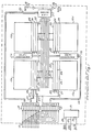
- FIG. 1 a block diagram of one example , a semiconductor read/write memory chip which may use segmented bit lines constructed according to the inventior is illustrated.
- This device is of the so-called 1-Megabit size, having 2 20 or 1,048,576 memory cells in an array of rows and columns.
- the array is partitioned into four identical b cks 10a, 10b, 10c and 10d, with each block containing 262 144 cells.
- Within eacn block there are 512 row lines, and all row lines are connected to one of the row decoders 1 or 11b.
- Each row decoder 11a or 11b receives 9-bits of a 10.bit row address from address input pins 12 by way of row add ess latches 13 and lines 14.
- a 10-bit column address is ,also applied to the input pins 12, in time-multiplexed manner and this column address is coupled to buffers 15.
- Eight data I/O lines 16 are positioned in the center of the array, anuone cf tnese eight is selected for data input or output y a 1-of-eight selector 17; a single 1/0 line from this selector 17 is connected through buffers to the data-in pin 18 anc the data-out pin 19.
- the selector 17 receives three bits of the column address by lines 20 from the column address buyers 15.
- Two of the eight lines 16 are connected respectivel to each of the blocks 10a, 10b, 10c and 10d, using four bits of the column address on lines 25 from buffers 15.
- Each one of 512 sense amplifiers 26 in each block is connected to one of the columns in the array; each column is made up of two column line halves or "bit lines", and each bit fire is selectively coupled to a number of bit line segments, according to the invention.
- Each buffer 24 is coupled to one of two columns; this selection is based on a one bit of the row address from buffers 13 on line 27.
- the memory device receives a row address strobe RAS on input pin 28, and a column address strobe CAS on input pin 29. Selection of a read or a write operation is made by a R/W control on an input pin 30.
- a clock generator and control circuit 31 produces all of the internal clocks and controls as needed.
- Each block of the array contains two rows of dummy cells 32 which are selectively coupled to the bit lines in the usual manner, as discussed in the above-mentioned Patents 4,293,993, or 4,081,701.
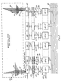
- the I/O lines 16, the first and second level intermediate output buffers 22 and 24, and the sense amplifiers 26 are shown in more detail for a part of one of the blocks 10a-lOd.
- buffers 22-1 through 22-8 are in one group of eight associated with one of the lines 16 for this block, and the buffers 22-9 through 22-16 are in another group of eight connected with the other one of the lines 16 for this block by lines 21.
- each sense amplifier 26 is connected to two of the bit lines 33, which in turn are selectively coupled to the bit line segments, as will be explained. Intersecting the bit lines 33 are 512 row lines 34 in the memory cell array. The dummy row lines 32 also intercept the bit lines 33, as will be described. One of the two dummy lines is selected by the row decoder Ila, 11b using one bit of the nine-bit row address 14.
- the tenth bit of the row address from buffers 13 is applied by the line 27 to a multiplex circuit for the sense amplifiers 26 to select which one of the two sense amplifiers of each pair is connected to the respective buffer 24 by 1ines 37.
- FIG. 3 a part of the circuitry of Fig. 2 is shown in more detail.
- the sense amplifiers 26 associated with the set of sixteen buffers 24-1 are shown. There are actually thirty-two sense amps 26 for this set. This set of sixteen buffers 24-1 is labeled 24-1-1 through 24-1-16 in this figure.
- Each individual sense amplifier 26 has two bit lines extending from it, in the so-called folded bit line configuration, and the bit line segments (not shown) run parallel to the bit lines 33.
- the row lines 34 intersect the bit lines, and memory cells are at intersections of row lines, and memory cells are at intersections of the row lines and bit line segments.
- a multiplexer 42 for each pair of sense amplifiers 26 selects one, based on the address bit on line 27, for connection to the respective buffer 24-1-1, 24-1-2, etc., by lines 37. Only one of the sixteen buffers 24-1-1 through 24-1-16 is selected at any one time, based on the four column address bits on lines 25, so only one will be operative to couple a read-or-write bit of data to or from the lines 38, 39 by lines 40.
- the buffer 22-1 of Fig. 3 may or may not be selected by the 2-of-16 select provided by three bits on lines 23, for coupling the dual-rail I/O lines 38, 39 to the single rail I/0 line 16 for this group.
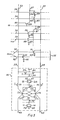
- Fig. 4 a detailed schematic diagram is shown for one of the buffers 24, e.g., the buffer 24-1-1 of Fig. 3, and for one of the buffers 22, e.g., the buffer 22-1.
- the multiplexer 42 consists of four transistors; one of the two transistors 43 is selected by the address bit on line 27 and its complement, i.e., by the sense-amp-select signals SAS1 and SAS2, so only one of these transistors 43 is on during a read (or write) operation. For read, only one path exists, through the selected one of the transistors 43. For write, one of the transistors 44 is also turned on by the address bit 27 which is Anded with a write control W from the control circuitry 31, valid when the R/W control 30 is in the write condition.
- the lines 45 which are inputs or outputs of the sense amplifiers 26 are single-ended for read and dual-rail for write; that is, for read operations both of the transistors 44 are off, and only one of the tranistors 43 is on, whereas for write operations one transistor 43 and its associated transistor 44 are conductive.
- the input/output lines 37 for the multiplexer 42 are connected through source/drain paths of transistors 46 and 47 in the buffer 24-1-1 to the lines 38 and 39.
- the transistors 46 and 47 are controlled by Y-select information on node 48, which comes from a 1-of-16 decoder 49 receiving the 4-bit column address on lines 25.
- a transistor 50 also is controlled by the Y-select on node 48; this transistor 50 is in series with an inverter transistor which has a P-channel precharge and load circuit.
- the inverter functions to place on node 51 the complement of the data bit on node 52, when the buffer 24-1-1 is selected (due to node 48 being high and transistor 50 being on), so the data bit from the selected sense amp is coupled from node 52 through the inverter, node 51, through transistor 47, line 39, to node 59 of the buffer 22-1.
- Transistor 46 and line 38 have no function during read operations. When node 52 is low, P-channel transistor 53 is on and node 51 is held at the supply voltage Vdd.
- node 51 when node 51 is low, P-channel transistor 54 is held on and node 52 is held high. Both nodes 51 and 52 are precharged high by P-channel transitors 55 which receive a low-going precharge voltage L (generated by the circuitry 31) in the precharge cycle after RAS goes high.
- the buffer 22-1 in Fig. 4 is controlled by Y-select information from address bits on lines 23 and a 2-of-16 decoder 56, so if this buffer is selected a node 57 is high.
- This condition turns on a transistor 58 and allows the data on line 39 or node 59 to be amplified through three stages 60, 61 and 62 for driving a node 63.
- a complementary transistor pair 64 is on, due to a read command R from control circuitry 31 applied to NAND gate 65. That is, when R/W is high, defining a read operation, then R is high and transistors 64 are both on. At this time, complementary transistor pairs 66 and 67 are off because write control W is low.
- the data bit on line 39 controls the line 16 through node 59, cascaded inverters 60, 61 and 62, node 63 and transistors 64, for a read operation.
- the transistor pairs 66 and 67 will be on, and transistor pair 64 will be off, so node 59 (and line 39) will receive the data bit from lne 16 through transistors 67, and node 63 (and lne 38) will receive the complement of this bit, thus converting from single-rail (on line 16) to double-rail (on lines 38, 39) during write.
- the dual-rail write data is coupled through both transistors 46 and 47, then through a selected transistor pair 43, 44, to one of the sense amps 26.
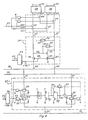
- FIG. 5 one of the sense amplifiers 26 is shown in detail. This figure also shows the two bit lines 33 for this sense amplifier and four of the 512 row lines 34 perpendiculr to these bit lines, along with two of the bit line segments according to the invention.
- the sense amplifier employs a CMOS cross-coupled flip-flop 70 having N-channel driver transistors 71 and P-channel transistors 72. Sense nodes 73 and 74 are connected to bit lines 33 through the source-drain paths of isolating transistors 75 and 76.
- a node 78 on the ground side of the flip-flop 70 is coupled to ground through two N-channel transistors 79 and 80 which have sense clocks Sl and S2 on their gates.
- the transistor 79 is much smaller than the transistor 80, and clock S1 occurs first, so the initial sensing is at a lower-gain condition, and is performed by N-channel transistors 71.
- a node 81 is coupled to the supply through P-channel transistors 82 and 83, one of which has sense clock S2 on its gate and the other a delayed S2D on its gate.
- the sense clock S2 is the complement of S2, so the P-channel transistors 72 start to operate only after the second clock S2 is activated.
- the transistor pairs 79,80 and 82,83 are shared with all of the other sense amplifiers 26 in two blocks 10a and 10b, i.e., 1024 sense amplifiers.
- the nodes 78 and 81 are precharged to Vref, about one-half Vdd by transistors (not shown) connected to the common lines when E is high.
- the bit lines 33 are precharged and equalized through three transistors 84 which have an equalize clock signal E on their gates; two of these transistors 84 have their sources connected to the reference voltage Vref.
- the value of this reference voltage is about half Vdd, so little or no net charge is needed from the chip supply Vdd to precharge all of the bit lines. That is, one line 33 will be high and the other low for each sense amplifier after an active cycle, so one will charge the other, and Vref need only supply any differential that might have occurred.
- the clock E is generated in the control circuitry 31 after the end of an active cycle, after RAS goes high.
- Each one of the memory cells consists of a capacitor 85 and an access transistor 86.
- the gates of all of the 512 access transistors 86 in a row are connected to (or formed by) a row line 34. Only one row line 34 of the 512 in the block is turned on at any one time, so only one memory cell capacitor 85 is selected. According to the invention, the selected cell is connected to a bit line 33 through a bit line segment 87.
- the row decoder lla or 11b selects the appropriate one of eight lines 89 by applying a segment select voltage SS to the selected line 89, at the same time as this decoder selects 1-of-512 row lines 34, based on certain ones of the same nine address bits from lines 14.
- dummy rows 32 a pair of dummy cells are provided for each pair of bit lines 33, and these dummy cells consist of dummy capacitors 90 and access transistors 91.
- the selected storage cell is coupled to the left-hand bit line 33 via selected segment 87 and transistor 88, then the right-hand dummy cell is selected in the row decoders lla, llb by one of the decoder output lines 92, and vice versa.
- One bit of the row address is used in the row decoder to select one or the other of these lines 92 of the dummy cell rows 32.
- An active cycle begins with the RAS voltage dropping from +5 to zero at the time TO.
- This example is a read cycle, so at time TO the R/W input voltage is at +5.
- the time prior to TO is a precharge cycle, during which the equalize signal E has been high, so all of the bit lines 33 and the nodes 78 and 81 have been precharged to the Vref voltage, assumed to be about 1/2 Vdd or +2.5.
- the segment select signal SS on all lines 89 is also held high during the precharge cycle, so all of the segments 87 are also precharged to the Vref voltage.
- the dropping of RAS at TO causes the equalize voltge E to drop, isolating the pairs of bit lines 33 from each other and from Vref.
- the segment select voltage SS then drops, isolating all of the segments 87 from the bit lines 33.
- the Xwd and Xdum voltages start to rise on the selected l-of-512 row line 34 and selected l-of-2 dummy line 92; at the same time, the segment-select signal on one of the lines 89 is brought up at T1.
- the sense amplifiers 26 are first activated by the Sl voltage going high, turning on the high-impedence N-channel transistor 79; this begins to separate the bit lines 33 further than the separation caused by the differential voltages on the storage cell and dummy cell. But before any current flows from the supply Vdd through transistors 72, the T voltage falls at T3, isolating the bitlines 33 from the sense nodes 73 and 74. After the T voltage falls, the sense voltage S2 is brought up, so the large tranistor 80 begins to conduct; also S2 drops, so one P-channel transistor 82 begins to conduct. After a slight delay S2D falls, and the other P-channel transistor 83 begins to conduct.
- each of the segment lines 89 is connected in common to all of the transistors 88 in a row, but a cell on a given segment 87 sees only the parasitic capacitance of that one segment line, plus that of one bit line 33.
- the advantage of using the segmented bit lines of the invention is that the parasitic capacitance of the bit lines 33 is much less than that of the segments 87; this is because the bit lines 33 are composed of metal strips separated from the substrate by a thick insulator coating, whereas the segments 87 are N+ regions within the substrate itself, as will be shown in Figs. 8 and 10A-10D.
- the capacitance ratio factor is greatly improved. Only one-thirty-secondth the amount of high-capacitance segment line is seen by a given storage cell, compared to using a full-length N+ bit line, and the metal bit hne 33 has perhaps only one-tenth the capacitance of an N+ diffused bit line. Also, the number of metal-to-silicon, or metal-to-poly, contacts per bit line or per row line is reduced to merely that of the number of transistors 88, since a "contactless" cell layout can be used.
- FIG. 8 One example of the one-transistor cell structure which may be used with the segmented bit lines of the invention is shown in Figs. 8, 9, and 10A-10D.
- the memory device of Figs. 1-7 is formed in a single silicon substrate 100 which would be about 180 x 500 mils in size, and about 15 mils thick.
- the small part shown in Figs. 8, 9 and '10A-10D is only about 5 x 5 microns.
- the word lines 34 are molybdenum strips extending above the face of the substrate 100, and the bit line segments 87 are elongated N+ regions in the substrate buried under thick thermal oxide 101.
- the capacitors 85 have upper plates 102 which are parts of a grounded polysilicon field plate 103 extending across the entire cell array.
- the silicon oxide 104 beneath the capacitor plate 102 is thinner than the insulator 105 beneath the other areas of the field plate 103.
- the gate 106 of a transistor 86 is formed by a part of the word line 34 where it extends into a hole 107 in the field plate 103.
- An oxide coating 108 covers the polysilicon field plate 103, insulating it from the word lines 34 and tranistor gates 106.
- a thin silicon oxide layer 109 is the gate insulator for the transistor.
- a thick layer 110 of deposited oxide or phosphosilicate glaze separates the aluminum lines 33 from the word lines 34; it is the thickness of this layer 110 which causes the parasitic capacitance of the bit lines to be small, compared to that of the N+ Segment lines 87.
- the pitch of the word lines 34 and the pitch of the bit lines 33 is therefore determined by the shape of the cell capacitor and transistor, rather than the contacts.
Landscapes
- Engineering & Computer Science (AREA)
- Microelectronics & Electronic Packaging (AREA)
- Computer Hardware Design (AREA)
- Semiconductor Memories (AREA)
- Dram (AREA)
Abstract
Description
- This invention relates to semiconductor memory devices, and more particularly to an improved cell array structure for dynamic read/write memory devices.
- Dynamic MOS read/write memory devices have been constructed generally as shown in U.S. Patent 4,081,701 (a 16K dynamic RAM) issued to White, McAdams, and Redwine, or U.S. Patent 4,239,993 (a 64K dynamic RAM) issued to McAlexander, White and Rao, both assigned to Texas Instruments. Improvements in photolithography and semiconductor processing have made possible the 256K DRAM which is now available, and the I-Megabit DRAM, now in development. All of these devices use a one-transistor storage cell in which the data is stored in a capacitor. In the devices of higher density, detecting the stored charge becomes more difficult because the cells are smaller and the bit lines longer, with more cells per bit line. A reliable signal cannot be detected by a differential sense amplifier when the ratio is less than about 1/30 or 1/40; preferably the ratio is in the area of 1/20 or less.
- Instead of the "open" bit line layout of Patents 4,081,701 and 4,239,993, the two bit lines for a given sense amplifier may be folded to lie adjacent one another on the face of the chip. In this manner, localized noise introduced into the substrate, as by alpha particles, for example, will be coupled equally to both bit lines and so will not affect the differential input to the sense amplifier. This folded bit line configuration can be detrimental to the capacitance ratio between storage capacitors and bit lines however, for some cell layouts, because the bit lines must be longer to accommodate twice the number of row lines on one side of a sense amplifier. That is, if the optimum cell width and length is such that a cell fits exactly with the pitch of bit lines and row lines for an open bit line configuration, then the same cell in a folded configuration will cause the bit lines to be longer, with more capacitance, because twice as many row lines must intercept a bit line.
- It is the principal object of this invention to provide an improved bit line an cell array structure for high density dynamic RAM devices, particularly MOS devices using one-transistor cells. Another object is to provide a high density dynamic RAM in which the ratio of storage capacitance to bit line capacitance is a maximum, in a folded bit line layout. Another object is to provide a high density dynamic RAM in which the ratio of storage capacitance to bit line capacitance is a maximum.
- In accordance with one embodiment of the invention, a semiconductor dynamic read/write memory device contains an array of rows and columns of one-transistor memory cells, with a differential sense amplifier for each column of cells. The sense amplifier has a pair of balanced bit lines extending from its inputs, in a folded bit line configuration. The memory cells are not directly connected to the bit lines, but instead are coupled to bit line segments. The row address selects a cell to be connected to a segment, and also selects one of two segments to be connected to one of two bit lines. The ratio of storage capacitance to effective bit line capacitance is increased, because the bit line itself is of lower capacitance to the substrate. Also, instead of being interleaved one-for-one, the word lines for cells to be connected to the two bit lines are in groups, one group for each segment line; the groups are interleaved. The combined segment line and bit line capacitance has a more favorable ratio to the storage capacitance, compared to the one-for-one interleaved layout.
- The novel features believed characteristic of the invention are set forth in the appended claims. The invention itself, however, as well as other features and advantages thereof, will be best understood by reference to the detailed description which follows, read in conjunction with the accompanying drawings, wherein:
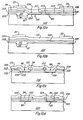
- Figure 1 is an electrical diagram in block form of a dynamic memory device of the I-Megabit size which may use a quasi-folded bit line configuration, with segmented bit lines in the cell array, according to the invention;
- Figure 2 is an electrical diagram in block form of a part of the memory device of Fig. 1;
- Figure 3 is an electrical diagram in block form of a part of the circuitry of Fig. 2;
- Figure 4 is an electrical diagram in schematic form of the multiplexers, buffers and column selector circuits of the device of Fig. 3;
- Figure 5 is an electrical diagram in schematic form of the sense amplifier and cell array of Figs. 1-4;
- Figure 6 is a timing diagram showing voltage vs. time for various nodes in the circuit of Figs. 1-5;
- Figure 7 is an enlarged view of a small part of the cell array showing the segmented bit lines of the invention;
- Figure 8 is a plan view, greatly enlarged, of a very small part of the cell array in the device of Figs. 1-7 showing two memory cells;
- Figure 9 is an electrical schematic diagram of the two cells of Fig. 8;
- Figures 10A-10D are elevation views in section of the device of Fig. 8, taken along the lines A-A and D-; respectively.
- Referring to Fig. 1, a block diagram of one example , a semiconductor read/write memory chip which may use segmented bit lines constructed according to the inventior is illustrated. This device is of the so-called 1-Megabit size, having 220 or 1,048,576 memory cells in an array of rows and columns. The array is partitioned into four identical b cks 10a, 10b, 10c and 10d, with each block containing 262 144 cells. Within eacn block, there are 512 row lines, and all row lines are connected to one of the
row decoders 1 or 11b. Each row decoder 11a or 11b receives 9-bits of a 10.bit row address from address input pins 12 by way of row add ess latches 13 andlines 14. A 10-bit column address is ,also applied to the input pins 12, in time-multiplexed manner and this column address is coupled tobuffers 15. Eight data I/O lines 16 are positioned in the center of the array, anuone cf tnese eight is selected for data input or output y a 1-of-eight selector 17; a single 1/0 line from this selector 17 is connected through buffers to the data-inpin 18 anc the data-out pin 19. The selector 17 receives three bits of the column address bylines 20 from thecolumn address buyers 15. Two of the eightlines 16 are connected respectivel to each of the blocks 10a, 10b, 10c and 10d, using four bits of the column address onlines 25 frombuffers 15. Each one of 512sense amplifiers 26 in each block is connected to one of the columns in the array; each column is made up of two column line halves or "bit lines", and each bit lire is selectively coupled to a number of bit line segments, according to the invention. Eachbuffer 24 is coupled to one of two columns; this selection is based on a one bit of the row address from buffers 13 online 27. - The memory device receives a row address strobe RAS on
input pin 28, and a column address strobeCAS on input pin 29. Selection of a read or a write operation is made by a R/W control on an input pin 30. A clock generator and control circuit 31 produces all of the internal clocks and controls as needed. - Each block of the array contains two rows of
dummy cells 32 which are selectively coupled to the bit lines in the usual manner, as discussed in the above-mentioned Patents 4,293,993, or 4,081,701. - Referring to Fig. 2, the I/
O lines 16, the first and second levelintermediate output buffers sense amplifiers 26 are shown in more detail for a part of one of the blocks 10a-lOd. In a given block, there are sixteen of theintermediate output buffers 22, in this figure labeled 22-1...22-16. Note that buffers 22-1 through 22-8 are in one group of eight associated with one of thelines 16 for this block, and the buffers 22-9 through 22-16 are in another group of eight connected with the other one of thelines 16 for this block bylines 21. For each one of the buffers 22-1...22-16, there is a set of sixteenbuffers 24; here these sets are labeled 24-1 through 24-16 (sixteen in each set). For each set of sixteenbuffers 24, a group of thirty-twosense amplifiers 26 is provided, and eachsense amplifier 26 is connected to two of thebit lines 33, which in turn are selectively coupled to the bit line segments, as will be explained. Intersecting thebit lines 33 are 512row lines 34 in the memory cell array. Thedummy row lines 32 also intercept thebit lines 33, as will be described. One of the two dummy lines is selected by the row decoder Ila, 11b using one bit of the nine-bit row address 14. - The tenth bit of the row address from buffers 13 is applied by the
line 27 to a multiplex circuit for thesense amplifiers 26 to select which one of the two sense amplifiers of each pair is connected to therespective buffer 24 by1ines 37. There are sixteen pairs of data/data-bar lines selected buffers 24 on one side bylines 40 and connected to theselected buffers 22 on the other side bylines 41. Note that the I/O changes from single-rail at the data I/O lines 16 to double rail at thelines - Referring to Fig. 3, a part of the circuitry of Fig. 2 is shown in more detail. The
sense amplifiers 26 associated with the set of sixteen buffers 24-1 are shown. There are actually thirty-twosense amps 26 for this set. This set of sixteen buffers 24-1 is labeled 24-1-1 through 24-1-16 in this figure. Eachindividual sense amplifier 26 has two bit lines extending from it, in the so-called folded bit line configuration, and the bit line segments (not shown) run parallel to the bit lines 33. The row lines 34 intersect the bit lines, and memory cells are at intersections of row lines, and memory cells are at intersections of the row lines and bit line segments. Amultiplexer 42 for each pair ofsense amplifiers 26 selects one, based on the address bit online 27, for connection to the respective buffer 24-1-1, 24-1-2, etc., bylines 37. Only one of the sixteen buffers 24-1-1 through 24-1-16 is selected at any one time, based on the four column address bits onlines 25, so only one will be operative to couple a read-or-write bit of data to or from thelines lines 40. The buffer 22-1 of Fig. 3 may or may not be selected by the 2-of-16 select provided by three bits onlines 23, for coupling the dual-rail I/O lines line 16 for this group. - Turning now to Fig. 4, a detailed schematic diagram is shown for one of the
buffers 24, e.g., the buffer 24-1-1 of Fig. 3, and for one of thebuffers 22, e.g., the buffer 22-1. - . The
multiplexer 42 consists of four transistors; one of the twotransistors 43 is selected by the address bit online 27 and its complement, i.e., by the sense-amp-select signals SAS1 and SAS2, so only one of thesetransistors 43 is on during a read (or write) operation. For read, only one path exists, through the selected one of thetransistors 43. For write, one of thetransistors 44 is also turned on by theaddress bit 27 which is Anded with a write control W from the control circuitry 31, valid when the R/W control 30 is in the write condition. Thus, thelines 45 which are inputs or outputs of thesense amplifiers 26 are single-ended for read and dual-rail for write; that is, for read operations both of thetransistors 44 are off, and only one of thetranistors 43 is on, whereas for write operations onetransistor 43 and its associatedtransistor 44 are conductive. The input/output lines 37 for themultiplexer 42 are connected through source/drain paths of transistors 46 and 47 in the buffer 24-1-1 to thelines node 48, which comes from a 1-of-16decoder 49 receiving the 4-bit column address onlines 25. Atransistor 50 also is controlled by the Y-select onnode 48; thistransistor 50 is in series with an inverter transistor which has a P-channel precharge and load circuit. In the single-ended read operation, the inverter functions to place on node 51 the complement of the data bit onnode 52, when the buffer 24-1-1 is selected (due tonode 48 being high andtransistor 50 being on), so the data bit from the selected sense amp is coupled fromnode 52 through the inverter, node 51, through transistor 47,line 39, tonode 59 of the buffer 22-1. Transistor 46 andline 38 have no function during read operations. Whennode 52 is low, P-channel transistor 53 is on and node 51 is held at the supply voltage Vdd. Likewise, when node 51 is low, P-channel transistor 54 is held on andnode 52 is held high. Bothnodes 51 and 52 are precharged high by P-channel transitors 55 which receive a low-going precharge voltage L (generated by the circuitry 31) in the precharge cycle after RAS goes high. - The buffer 22-1 in Fig. 4 is controlled by Y-select information from address bits on
lines 23 and a 2-of-16decoder 56, so if this buffer is selected anode 57 is high. This condition turns on atransistor 58 and allows the data online 39 ornode 59 to be amplified through threestages node 63. For read, acomplementary transistor pair 64 is on, due to a read command R from control circuitry 31 applied toNAND gate 65. That is, when R/W is high, defining a read operation, then R is high andtransistors 64 are both on. At this time, complementary transistor pairs 66 and 67 are off because write control W is low. Thus, the data bit online 39 controls theline 16 throughnode 59, cascadedinverters node 63 andtransistors 64, for a read operation. On the other hand, for a write operation, the transistor pairs 66 and 67 will be on, andtransistor pair 64 will be off, so node 59 (and line 39) will receive the data bit fromlne 16 throughtransistors 67, and node 63 (and lne 38) will receive the complement of this bit, thus converting from single-rail (on line 16) to double-rail (onlines 38, 39) during write. From thelines transistor pair sense amps 26. - Referring to Fig. 5, one of the
sense amplifiers 26 is shown in detail. This figure also shows the twobit lines 33 for this sense amplifier and four of the 512row lines 34 perpendiculr to these bit lines, along with two of the bit line segments according to the invention. The sense amplifier employs a CMOS cross-coupled flip-flop 70 having N-channel driver transistors 71 and P-channel transistors 72.Sense nodes lines 33 through the source-drain paths of isolating transistors 75 and 76. - A node 78 on the ground side of the flip-flop 70 is coupled to ground through two N-
channel transistors 79 and 80 which have sense clocks Sl and S2 on their gates. The transistor 79 is much smaller than thetransistor 80, and clock S1 occurs first, so the initial sensing is at a lower-gain condition, and is performed by N-channel transistors 71. On the Vdd side, a node 81 is coupled to the supply through P-channel transistors 82 and 83, one of which has sense clock S2 on its gate and the other a delayed S2D on its gate. The sense clock S2 is the complement of S2, so the P-channel transistors 72 start to operate only after the second clock S2 is activated. There is a two-interval sense operation, first Sl, then S2 and S2. The transistor pairs 79,80 and 82,83 are shared with all of theother sense amplifiers 26 in two blocks 10a and 10b, i.e., 1024 sense amplifiers. The nodes 78 and 81 are precharged to Vref, about one-half Vdd by transistors (not shown) connected to the common lines when E is high. - The bit lines 33 are precharged and equalized through three
transistors 84 which have an equalize clock signal E on their gates; two of thesetransistors 84 have their sources connected to the reference voltage Vref. The value of this reference voltage is about half Vdd, so little or no net charge is needed from the chip supply Vdd to precharge all of the bit lines. That is, oneline 33 will be high and the other low for each sense amplifier after an active cycle, so one will charge the other, and Vref need only supply any differential that might have occurred. The clock E is generated in the control circuitry 31 after the end of an active cycle, after RAS goes high. - Each one of the memory cells consists of a
capacitor 85 and anaccess transistor 86. There are 512 cells for each column, i.e., associated with a pair of bit lines 33. Also, there are 512 cells for each row, i.e., associated with eachrow line 34. The gates of all of the 512access transistors 86 in a row are connected to (or formed by) arow line 34. Only onerow line 34 of the 512 in the block is turned on at any one time, so only onememory cell capacitor 85 is selected. According to the invention, the selected cell is connected to abit line 33 through abit line segment 87. In order to reduce the ratio of the bit line capacitance to the value of thestorage capacitance 85, a number ofbit line segments 87 are employed for each pair of bit lines 33. Two of thesesegments 87 are coupled toopposite bit lines 33 at a given time by twotransistors 88. For example, eachsegment 87 may have thirty-two cells connected to it, so in the embodiment disclosed herein there must be sixteen of thesesegments 87 for each sense amplifier (16 x 32 = 512). The row decoder lla or 11b selects the appropriate one of eightlines 89 by applying a segment select voltage SS to the selectedline 89, at the same time as this decoder selects 1-of-512row lines 34, based on certain ones of the same nine address bits fromlines 14. When aline 89 goes high, twosegments 87 are connected to bitlines 33, one on each side by the twotransistors 88, but only one of thesesegments 87 will have an activatedrow line 34 on it, so only one memory cell is coupled to abit line 33. - In the
dummy rows 32, a pair of dummy cells are provided for each pair ofbit lines 33, and these dummy cells consist of dummy capacitors 90 and access transistors 91. When the selected storage cell is coupled to the left-hand bit line 33 via selectedsegment 87 andtransistor 88, then the right-hand dummy cell is selected in the row decoders lla, llb by one of thedecoder output lines 92, and vice versa. One bit of the row address is used in the row decoder to select one or the other of theselines 92 of thedummy cell rows 32. - Referring to Fig. 6, the sequence of operation of the memory device will be explained for a single-bit read operation. An active cycle begins with the RAS voltage dropping from +5 to zero at the time TO. This example is a read cycle, so at time TO the R/W input voltage is at +5. The time prior to TO is a precharge cycle, during which the equalize signal E has been high, so all of the bit lines 33 and the nodes 78 and 81 have been precharged to the Vref voltage, assumed to be about 1/2 Vdd or +2.5. The segment select signal SS on all
lines 89 is also held high during the precharge cycle, so all of thesegments 87 are also precharged to the Vref voltage. The dropping of RAS at TO causes the equalize voltge E to drop, isolating the pairs ofbit lines 33 from each other and from Vref. The segment select voltage SS then drops, isolating all of thesegments 87 from the bit lines 33. As soon as the row decoders lla, llb have had time to respond to the row address, the Xwd and Xdum voltages start to rise on the selected l-of-512row line 34 and selected l-of-2dummy line 92; at the same time, the segment-select signal on one of thelines 89 is brought up at T1. These address voltages Xwd, Xdum and SS are brought up rather slowly, and, after reaching the Vdd level, SS and Xwd are boosted above Vdd to eliminate the Vt drop across the access tranistors 86 and 88. The Xdum voltage falls, since the function of the dummy cells is completed during initial sensing, and the dummy capacitors can be decoupled from the bit lines so that precharge of these capacitors can begin. - At time T2, the
sense amplifiers 26 are first activated by the Sl voltage going high, turning on the high-impedence N-channel transistor 79; this begins to separate the bit lines 33 further than the separation caused by the differential voltages on the storage cell and dummy cell. But before any current flows from the supply Vdd throughtransistors 72, the T voltage falls at T3, isolating thebitlines 33 from thesense nodes large tranistor 80 begins to conduct; also S2 drops, so one P-channel transistor 82 begins to conduct. After a slight delay S2D falls, and the other P-channel transistor 83 begins to conduct. After S2 rises and S2 drops at T4, the T voltage is brought up to Vdd. At time T5 after the isolating transistors 75, 76 have been turned back on, sensing is complete and onebit line 33 is high and the other at zero, so the sense-amp-select signal S AS1 or SAS2 is turned on, connecting one of the bit lines to thenode 52 vialines decoders nodes line 16, and shortly thereafter valid on the output pin 19. - With reference to Fig. 7, a small part of one block of the cell array is illustrated. Each of the segment lines 89 is connected in common to all of the
transistors 88 in a row, but a cell on a givensegment 87 sees only the parasitic capacitance of that one segment line, plus that of onebit line 33. The advantage of using the segmented bit lines of the invention is that the parasitic capacitance of the bit lines 33 is much less than that of thesegments 87; this is because the bit lines 33 are composed of metal strips separated from the substrate by a thick insulator coating, whereas thesegments 87 are N+ regions within the substrate itself, as will be shown in Figs. 8 and 10A-10D. Thus, even though the length of thebit line 33 to which the selectedcapacitor 85 is coupled is as long as if the segmenting had not been used, nevertheless the capacitance ratio factor is greatly improved. Only one-thirty-secondth the amount of high-capacitance segment line is seen by a given storage cell, compared to using a full-length N+ bit line, and themetal bit hne 33 has perhaps only one-tenth the capacitance of an N+ diffused bit line. Also, the number of metal-to-silicon, or metal-to-poly, contacts per bit line or per row line is reduced to merely that of the number oftransistors 88, since a "contactless" cell layout can be used. - One example of the one-transistor cell structure which may be used with the segmented bit lines of the invention is shown in Figs. 8, 9, and 10A-10D. The memory device of Figs. 1-7 is formed in a
single silicon substrate 100 which would be about 180 x 500 mils in size, and about 15 mils thick. The small part shown in Figs. 8, 9 and '10A-10D is only about 5 x 5 microns. The word lines 34 are molybdenum strips extending above the face of thesubstrate 100, and thebit line segments 87 are elongated N+ regions in the substrate buried under thickthermal oxide 101. Thecapacitors 85 haveupper plates 102 which are parts of a groundedpolysilicon field plate 103 extending across the entire cell array. Thesilicon oxide 104 beneath thecapacitor plate 102 is thinner than theinsulator 105 beneath the other areas of thefield plate 103. Thegate 106 of atransistor 86 is formed by a part of theword line 34 where it extends into ahole 107 in thefield plate 103. Anoxide coating 108 covers thepolysilicon field plate 103, insulating it from the word lines 34 andtranistor gates 106. A thinsilicon oxide layer 109 is the gate insulator for the transistor. Athick layer 110 of deposited oxide or phosphosilicate glaze separates thealuminum lines 33 from the word lines 34; it is the thickness of thislayer 110 which causes the parasitic capacitance of the bit lines to be small, compared to that of the N+ Segment lines 87. Every thirty-two cells there is a metal-to-silicon contact (not shown) between themetal lines 33 and an N+ region in thesubstrate 100 to contact the drain of atransistor 88; this contact is at a hole in thethick insulator 110 andfield plate 103. Note, however, that no contacts are needed for the cells, only for the segment lines. The pitch of the word lines 34 and the pitch of the bit lines 33 is therefore determined by the shape of the cell capacitor and transistor, rather than the contacts. - Although the embodiment disclosed herein is a dynamic read/write memory, features of the invention are applicable to read-only memories such as ROMs or EPROMs, as well as to other read/write memories such as static RAMs.
- While this invention has been described with reference to an illustrative embodiment, this description is not intended to be construed in a liminting sense. Various modifications to the illustrative embodiment, as well as other embodiments of the invention, will be apparent to persons skilled in the art upon reference to this description. It is therefore contemplated that the appended claims will cover any such modifications or embodiments as fall within the true scope of the invention.
Claims (17)
and control means for each of said segments for selectively connecting each said segment to a bit line.
and control means selectively connecting said segments to said bit line.
Applications Claiming Priority (4)
| Application Number | Priority Date | Filing Date | Title |
|---|---|---|---|
| US06/634,898 US4658377A (en) | 1984-07-26 | 1984-07-26 | Dynamic memory array with segmented bit lines |
| US06/634,899 US4701885A (en) | 1984-07-26 | 1984-07-26 | Dynamic memory array with quasi-folded bit lines |
| US634899 | 1984-07-26 | ||
| US634898 | 1984-07-26 |
Publications (3)
| Publication Number | Publication Date |
|---|---|
| EP0169460A2 true EP0169460A2 (en) | 1986-01-29 |
| EP0169460A3 EP0169460A3 (en) | 1988-05-18 |
| EP0169460B1 EP0169460B1 (en) | 1991-05-15 |
Family
ID=27092256
Family Applications (1)
| Application Number | Title | Priority Date | Filing Date |
|---|---|---|---|
| EP85108720A Expired EP0169460B1 (en) | 1984-07-26 | 1985-07-12 | Dynamic memory array with segmented and quasi-folded bit lines |
Country Status (3)
| Country | Link |
|---|---|
| EP (1) | EP0169460B1 (en) |
| JP (1) | JPS63127490A (en) |
| DE (1) | DE3582828D1 (en) |
Cited By (4)
| Publication number | Priority date | Publication date | Assignee | Title |
|---|---|---|---|---|
| GB2246001A (en) * | 1990-04-11 | 1992-01-15 | Digital Equipment Corp | Cache memory having sub-arrays of cells |
| EP0544320A2 (en) * | 1991-11-27 | 1993-06-02 | Kabushiki Kaisha Toshiba | Semiconductor memory cell |
| WO1997009719A1 (en) * | 1995-09-07 | 1997-03-13 | Advanced Micro Devices, Inc. | Segmented read line circuit particularly useful for multi-port storage arrays |
| US7110319B2 (en) * | 2004-08-27 | 2006-09-19 | Micron Technology, Inc. | Memory devices having reduced coupling noise between wordlines |
Citations (2)
| Publication number | Priority date | Publication date | Assignee | Title |
|---|---|---|---|---|
| EP0068645A2 (en) * | 1981-05-29 | 1983-01-05 | Hitachi, Ltd. | A semiconductor device |
| EP0077935A2 (en) * | 1981-10-23 | 1983-05-04 | Kabushiki Kaisha Toshiba | Dynamic memory device |
Family Cites Families (2)
| Publication number | Priority date | Publication date | Assignee | Title |
|---|---|---|---|---|
| JPS60234296A (en) * | 1984-05-07 | 1985-11-20 | Hitachi Ltd | Semiconductor memory |
| JPS60253096A (en) * | 1984-05-30 | 1985-12-13 | Fujitsu Ltd | Semiconductor storage device |
-
1985
- 1985-07-12 DE DE8585108720T patent/DE3582828D1/en not_active Expired - Lifetime
- 1985-07-12 EP EP85108720A patent/EP0169460B1/en not_active Expired
-
1987
- 1987-06-30 JP JP62163875A patent/JPS63127490A/en active Granted
Patent Citations (2)
| Publication number | Priority date | Publication date | Assignee | Title |
|---|---|---|---|---|
| EP0068645A2 (en) * | 1981-05-29 | 1983-01-05 | Hitachi, Ltd. | A semiconductor device |
| EP0077935A2 (en) * | 1981-10-23 | 1983-05-04 | Kabushiki Kaisha Toshiba | Dynamic memory device |
Cited By (10)
| Publication number | Priority date | Publication date | Assignee | Title |
|---|---|---|---|---|
| GB2246001A (en) * | 1990-04-11 | 1992-01-15 | Digital Equipment Corp | Cache memory having sub-arrays of cells |
| GB2246001B (en) * | 1990-04-11 | 1994-06-15 | Digital Equipment Corp | Array architecture for high speed cache memory |
| EP0544320A2 (en) * | 1991-11-27 | 1993-06-02 | Kabushiki Kaisha Toshiba | Semiconductor memory cell |
| EP0544320A3 (en) * | 1991-11-27 | 1994-04-06 | Toshiba Kk | |
| US5500815A (en) * | 1991-11-27 | 1996-03-19 | Kabushiki Kaisha Toshiba | Semiconductor memory |
| WO1997009719A1 (en) * | 1995-09-07 | 1997-03-13 | Advanced Micro Devices, Inc. | Segmented read line circuit particularly useful for multi-port storage arrays |
| US5646893A (en) * | 1995-09-07 | 1997-07-08 | Advanced Micro Devices, Inc. | Segmented read line circuit particularly useful for multi-port storage arrays |
| US7110319B2 (en) * | 2004-08-27 | 2006-09-19 | Micron Technology, Inc. | Memory devices having reduced coupling noise between wordlines |
| US7417916B2 (en) | 2004-08-27 | 2008-08-26 | Micron Technology, Inc. | Methods of reducing coupling noise between wordlines |
| US7460430B2 (en) | 2004-08-27 | 2008-12-02 | Micron Technology, Inc. | Memory devices having reduced coupling noise between wordlines |
Also Published As
| Publication number | Publication date |
|---|---|
| EP0169460B1 (en) | 1991-05-15 |
| JPS63127490A (en) | 1988-05-31 |
| JPH0542077B2 (en) | 1993-06-25 |
| DE3582828D1 (en) | 1991-06-20 |
| EP0169460A3 (en) | 1988-05-18 |
Similar Documents
| Publication | Publication Date | Title |
|---|---|---|
| US4658377A (en) | Dynamic memory array with segmented bit lines | |
| US5416734A (en) | Bit line structure for semiconductor memory device | |
| US6600671B2 (en) | Reduced area sense amplifier isolation layout in a dynamic RAM architecture | |
| US6108264A (en) | Dynamic type semiconductor memory device | |
| KR101156172B1 (en) | Semiconductor integrated circuit device | |
| US5682343A (en) | Hierarchical bit line arrangement in a semiconductor memory | |
| US5111434A (en) | Semiconductor memory device | |
| KR970000883B1 (en) | Semiconductor memory device having dual word line structure | |
| US4551820A (en) | Dynamic RAM integrated circuit device | |
| US4800525A (en) | Dual ended folded bit line arrangement and addressing scheme | |
| US5815428A (en) | Semiconductor memory device having hierarchical bit line structure | |
| US5127739A (en) | CMOS sense amplifier with bit line isolation | |
| KR900005667B1 (en) | Semiconductor memory device | |
| US4195357A (en) | Median spaced dummy cell layout for MOS random access memory | |
| US4608670A (en) | CMOS sense amplifier with N-channel sensing | |
| US4627033A (en) | Sense amplifier with reduced instantaneous power | |
| EP0264929B1 (en) | Semiconductor memory device with improved bit line arrangement | |
| US5091887A (en) | Dynamic semiconductor memory device | |
| US4701885A (en) | Dynamic memory array with quasi-folded bit lines | |
| US4418399A (en) | Semiconductor memory system | |
| US4630240A (en) | Dynamic memory with intermediate column derode | |
| US5295111A (en) | Dynamic random access memory device with improved power supply system for speed-up of rewriting operation on data bits read-out from memory cells | |
| US4198697A (en) | Multiple dummy cell layout for MOS random access memory | |
| USRE33694E (en) | Dynamic memory array with segmented bit lines | |
| JPH07135301A (en) | Semiconductor memory |
Legal Events
| Date | Code | Title | Description |
|---|---|---|---|
| PUAI | Public reference made under article 153(3) epc to a published international application that has entered the european phase |
Free format text: ORIGINAL CODE: 0009012 |
|
| AK | Designated contracting states |
Designated state(s): DE FR GB |
|
| PUAL | Search report despatched |
Free format text: ORIGINAL CODE: 0009013 |
|
| AK | Designated contracting states |
Kind code of ref document: A3 Designated state(s): DE FR GB |
|
| 17P | Request for examination filed |
Effective date: 19881012 |
|
| 17Q | First examination report despatched |
Effective date: 19900316 |
|
| GRAA | (expected) grant |
Free format text: ORIGINAL CODE: 0009210 |
|
| AK | Designated contracting states |
Kind code of ref document: B1 Designated state(s): DE FR GB |
|
| REF | Corresponds to: |
Ref document number: 3582828 Country of ref document: DE Date of ref document: 19910620 |
|
| ET | Fr: translation filed | ||
| PLBE | No opposition filed within time limit |
Free format text: ORIGINAL CODE: 0009261 |
|
| STAA | Information on the status of an ep patent application or granted ep patent |
Free format text: STATUS: NO OPPOSITION FILED WITHIN TIME LIMIT |
|
| 26N | No opposition filed | ||
| REG | Reference to a national code |
Ref country code: GB Ref legal event code: IF02 |
|
| PGFP | Annual fee paid to national office [announced via postgrant information from national office to epo] |
Ref country code: GB Payment date: 20040615 Year of fee payment: 20 |
|
| PGFP | Annual fee paid to national office [announced via postgrant information from national office to epo] |
Ref country code: FR Payment date: 20040702 Year of fee payment: 20 |
|
| PGFP | Annual fee paid to national office [announced via postgrant information from national office to epo] |
Ref country code: DE Payment date: 20040730 Year of fee payment: 20 |
|
| PG25 | Lapsed in a contracting state [announced via postgrant information from national office to epo] |
Ref country code: GB Free format text: LAPSE BECAUSE OF EXPIRATION OF PROTECTION Effective date: 20050711 |
|
| REG | Reference to a national code |
Ref country code: GB Ref legal event code: PE20 |