EP0169360A2 - Random access memory - Google Patents
Random access memory Download PDFInfo
- Publication number
- EP0169360A2 EP0169360A2 EP85107232A EP85107232A EP0169360A2 EP 0169360 A2 EP0169360 A2 EP 0169360A2 EP 85107232 A EP85107232 A EP 85107232A EP 85107232 A EP85107232 A EP 85107232A EP 0169360 A2 EP0169360 A2 EP 0169360A2
- Authority
- EP
- European Patent Office
- Prior art keywords
- bit
- transistor
- word
- lines
- collector
- Prior art date
- Legal status (The legal status is an assumption and is not a legal conclusion. Google has not performed a legal analysis and makes no representation as to the accuracy of the status listed.)
- Granted
Links
Images


Classifications
-
- G—PHYSICS
- G11—INFORMATION STORAGE
- G11C—STATIC STORES
- G11C11/00—Digital stores characterised by the use of particular electric or magnetic storage elements; Storage elements therefor
- G11C11/21—Digital stores characterised by the use of particular electric or magnetic storage elements; Storage elements therefor using electric elements
- G11C11/34—Digital stores characterised by the use of particular electric or magnetic storage elements; Storage elements therefor using electric elements using semiconductor devices
- G11C11/40—Digital stores characterised by the use of particular electric or magnetic storage elements; Storage elements therefor using electric elements using semiconductor devices using transistors
- G11C11/41—Digital stores characterised by the use of particular electric or magnetic storage elements; Storage elements therefor using electric elements using semiconductor devices using transistors forming static cells with positive feedback, i.e. cells not needing refreshing or charge regeneration, e.g. bistable multivibrator or Schmitt trigger
- G11C11/413—Auxiliary circuits, e.g. for addressing, decoding, driving, writing, sensing, timing or power reduction
- G11C11/414—Auxiliary circuits, e.g. for addressing, decoding, driving, writing, sensing, timing or power reduction for memory cells of the bipolar type
- G11C11/415—Address circuits
-
- G—PHYSICS
- G11—INFORMATION STORAGE
- G11C—STATIC STORES
- G11C11/00—Digital stores characterised by the use of particular electric or magnetic storage elements; Storage elements therefor
- G11C11/21—Digital stores characterised by the use of particular electric or magnetic storage elements; Storage elements therefor using electric elements
- G11C11/34—Digital stores characterised by the use of particular electric or magnetic storage elements; Storage elements therefor using electric elements using semiconductor devices
- G11C11/40—Digital stores characterised by the use of particular electric or magnetic storage elements; Storage elements therefor using electric elements using semiconductor devices using transistors
- G11C11/41—Digital stores characterised by the use of particular electric or magnetic storage elements; Storage elements therefor using electric elements using semiconductor devices using transistors forming static cells with positive feedback, i.e. cells not needing refreshing or charge regeneration, e.g. bistable multivibrator or Schmitt trigger
- G11C11/413—Auxiliary circuits, e.g. for addressing, decoding, driving, writing, sensing, timing or power reduction
- G11C11/414—Auxiliary circuits, e.g. for addressing, decoding, driving, writing, sensing, timing or power reduction for memory cells of the bipolar type
- G11C11/416—Read-write [R-W] circuits
Definitions
- the invention is directed to an array of memory cells.
- Random access memories employing CTS type memory cells are known to the art. See for the example, the Gersbach patent 3,863,229, the Dorler et al IBM TDB publication "AC Write Scheme For Bipolar Random-Access Memories Using Schottky Coupled Cells", IBM TDB, Vol. 23, No. 11, April 1981, pages 4960-2, and the Dorler et al Article “A 1024 Byte ECL Random Access Memory Using a Complementary Transistor Switch (CTS) Cell", IBM Journal of Research and Development, Vol. 25, No. 3, May 1981, pages 126-34.
- CTS Complementary Transistor Switch
- bit decode transistor has to drive a number of bit columns across the chip. Due to long metal line and large fan-out current, voltage drop along the bit decode line is high. The cells at the end of the bit decode line may have insufficient voltage across their "1" bit rail resistors to provide adequate gate currents into the cells. This may lead to potential data retention problems on the selected cells.
- both selection and deselection of the bit rails are slow due to the fact that the bit decode transistor has large fan-out loadings. Discharge speed of the bit rails is limited by the bit rail resistors.
- the bit selection scheme in accordance with the invention obviates the above recited short comings of known RAMs and in particular RAMs using CTS cells.
- the word lines are very capacitive. (For word lines having 60 to 80 cells, this word line capacitance could be as high as 30 to 40 pf).
- a constant current source pulls down the selected word lines according to its large RC time constant. Hence cell selection is very slow, and its drive capability is often limited by the fixed source of current.
- bit line voltage of the side to be written a "1" is driven high. This causes the bit rail and the drain line levels to rise.
- a long address set up time is needed to wait for the previous selected cell to get out of the way before writing can start in order to avoid write-through problems.
- the object of the invention is to provide an improved random access memory which employs complementary transistor switch (CTS) memory cells, which obviates data retention concerns on fully selected cells, and improves (1) speed of selection of word lines, (2) stability of selected word lines, and (3) reduces address set-up time for "write" operation.
- CTS complementary transistor switch
- the bit select circuitry includes interconnected first and second level matrix decoders, each memory column has a pair of bit lines, each pair of bit lines has connected thereto bit select circuit means, each of said bit select circuit means being connected to an output of said second level decoder, a bit up level clamp circuit connected to each of said bit select circuit means of each pair of bit lines, each of said bit select circuit means including first circuit means for increasing the speed of selection of the selected pair of bit lines, said bit up level clamp circuit cooperating with said bit select circuit means of said selected pair of bit lines for positively limiting the upper potential level of said selected pair of bit lines, and each of said bit select circuit means including second circuit means for increasing the speed of deselection of the selected pair of bit lines.
- the invention also includes voltage mode word selection means in a RAM preferably employing CTS type memory cells.
- the word lines are very capacitive. (For word lines having 60 to 80 cells, this word line capacitance could be as high as 30 to 40 pf).
- a constant current source pulls down the selected word line according to its large RC time constant. Hence, cell selection is very slow, and its drive capability is often limited by the fixed source of current.
- bit line voltage of the side to be written a "1" is driven high. This causes the bit rail and the drain line levels to rise.
- a long address set up time is needed to wait for the previous selected cell to go out of the way before writing can start in order to avoid write-through problems.
- Figure 2 shows a lk x 4 RAM in accordance with the invention.
- This RAM has an array density of 4096 cells arranged in 64 words (rows) by 64 bit (columns). The 64 bit columns are further divided into 4 data groups, so that it will write 4 bits (therefore 4 data inputs) and read 4 bits (4 data outputs) at a time.
- the RAM has 6 word addresses (to select 1 out of 64 rows) and 4 bit addresses (to select 4 out of 64 bits). Read and write operations are controlled by the RW input.
- the first level decode includes two groups of 4 address lines (BAO - BA3 and BA4 - BA7) formed from output emitter dotting of the four bit address receivers.
- the bit address receivers are current switch emitter follower circuits as shown in Figure 4. They convert the address inputs to true and complement signals. By means of emitter follower output dotting of the address receiver pairs, a partial decode of 1 out of 4 is formed from each group, hence, giving a total of two selected (low level) lines.
- the second level decode function is performed by the 16 bit decoders ( Figure 5), which have current switch inputs and high speed push-pull outputs.
- Input 1 of the bit decoder is connected to one of the 4 lines in BAO - BA3 address group, and input 2 is connected to one in the BA4 - BA7 group.
- Of the 16 BD output lines only one is decoded to a selected up level. Each BD line fans out to drive four bit columns (one from each data group), so that four cells are selected at a time for READ or WRITE operation.
- Each bit column has a bit select circuit ( Figures 3 and 6) to perform bit line select and deselect functions.
- the selected bit lines up level is set by a bit up level clamp circuit (Bit UPCL, Figure 7), so that the cells' read and write operating points can be readily adjusted by changing the up clamp (UC) level.
- the SCR device For unclamped CTS cell, the SCR device operates in saturation mode.
- the cell is more capacitive (due to higher B-C junction saturation capacitance) than a normal CTS with Schottky clamp. This makes the unclamped cell very difficult to write.
- the bit select circuit It is essential that the bit select circuit is capable of driving high transient current into the cell to enable fast write performance.
- a novel circuit technique utilizing capacitive boot strapping and transient drive mechanism is designed for this application. The bit select circuit's modes of operation are described below.
- the BD line is held low by its corresponding bit decoder to a voltage close to V N .
- Transistors T1 and T2 of the bit select circuit are driven into inverse saturated mode operation. Nodes 1 and 2 are clamped low by the B-C junctions of Tl and T2 to a voltage a V BC above the BD level. Nodes 3 and 4 are also driven negative by the inverse transistors to a voltage close to that of the BD line (a V CES above from BD). With nodes 1, 2, 3 and 4 being held low, transistors T3, T4 and T5, T6 are shut off. No current will flow into the bit rail resistors RBL and RBR. The bit lines BL and BR levels are equal to those of nodes 3 and 4.
- resistors R1 and R2 provide small amount of base currents that conducts through Tl and T2 into the BD line. Since Tl and T2 conducts in inverse saturation mode, they develop large diffusion capacitance (due to storage charge) across their B-C and B-E junctions. These storage charges will be used to boot strap nodes 1, 2 and nodes 3, 4 up rapidly when the BD line is selected high.
- both the PDL and PDR lines are high (up at around Vp).
- Nodes 1 and 2's up levels are clamped by the transistor diodes T5 and T6 respectively to a voltage set by the UC line (see Figure 12).
- the read reference level on the UC line is generated by the bit up level clamp circuit in such a way that it tracks with the selected cells' voltages to ensure proper read currents (load current I L and gate current I G).
- the cell's read currents are supplied by T1 and T2 through resistors RBL and RBR.
- Typical READ currents are set at I L ⁇ 1.0 mA and I G ⁇ 0.2 mA. This results in a voltage differential of about 600-700 mV across the bit lines for read sensing by the sense amplifier.
- Tl and T2 operate in active forward mode to provide DC read currents.
- Transistors T3 and T4 are only turned ON transiently. They will stay OFF after the bit lines BL and BR reach their fully selected up levels. Since the BD line's voltage level is set to be higher than those of nodes 1 and 2, transistors Tl and T2 in the selected state are always kept in active forward conduction.
- the read currents are defined by the read reference level and will not be affected by the BD's voltage variations or line drops.
- bit line selection is similar to that of the READ as described above. The only difference here is that one of the write control lines (either PDL or PDR, depending on the data to be written) is driven negative to a voltage close to V N . by the write control circuit prior to bit selection (see Figure 13). The lowered PDL or PDR line will clamp down either node 1 or 2 through the transistor diode T5 or T6 respectively, so that when the bit rail is selected, only one side of the bit lines will be driven high to provide write current into the cell. The other side will stay at down level in order to shut off the bit line current that normally flows into the cell.
- This mode of write operation is denoted "Differential Mode Write" hereinafter.
- node 1 or 2's up level is also clamped by the transistor diode T5 or T6 to a voltage set by the UC line.
- the write reference voltage is typically 600-800 mV above the READ reference voltage, so that sufficient over voltage and sufficient write current are-always guaranteed to provide fast write performance.
- writing is primarily done by driving large transient current into the cell to overcome its original state. This large transient write current (typically a few milli ampere) is sourced by either T3 or T4 from V directly. After the cell has been written, its bit line voltage will rise up to the "1" level. Transistor T3 or T4 will be gradually turned off to remove the large transient write current.
- Resistor RBL or RBR will then supply a small DC write current I W from either Tl or T2 to reinforce the state of the newly written cell.
- the large transient write current is sourced directly from V P through T3 or T4. The write performance is therefore not affected by the BD line's level variation.
- Transistors T1 and T2 of the bit select circuit are driven into inverse saturation mode. Nodes 1, 2 and 3, 4 are pulled negative to shut off the read or write bit rail currents.
- the bit lines are also pulled down actively by Schottky diodes SL and SR and will discharge into the BD line. While diodes SL and SR are pulling down the bit lines, the bit rail resistors RBL and RBR are also driven low by the inverse transistors to discharge the bit lines. After the bit lines are fully discharged to their unselect down levels, resistors RBL, RBR and diodes SL, SR will stop conducting. The bit column is now said to be in an unselected state.
- the disclosed bit select scheme has particular utility in arrays using CTS (Complementary Transistor Switch, Figure lA) cells. With this scheme, at least the following two advantages have been achieved over the known designs.
- the improved bit selection circuit means in accordance with the invention includes the following elements:
- the first level decode includes three groups of 4 address lines (WA4 -.WA3, WAO - WA7, and WA8 - WA11) formed from output emitter dotting of the 6 word address receivers.
- the word address receivers are current switch emitter follower circuits ( Figure 4). They convert the address inputs to true and complement signals. By means of emitter follower output dotting of the address receiver pairs, a partial decode of 1 out of 4 is obtained from each group, hence giving a total of three selected (low level) lines.
- the second level decode function is performed by the 64 word decoders ( Figure 9).
- Each word decoder has three current switch inputs (IN1 - IN3) and two high speed high power push-pull outputs (WL and DL).
- IN1 of the word decoder is connected to one of the four lines in WAO - WA3 address group.
- IN2 is connected to one in the second group (WA4 - WA7), and
- IN3 is connected to one in the third group (WA8 - WAll). All these three inputs have to be low in order to select a row line.
- the two outputs of the word decoder are connected to the word line (WL) and drain line (DL) of the memory cells as shown.
- An unselected word decoder will have at least one of its three inputs high.
- Decoding transistors T1, T2 or T3 are turned ON to pull down node 1.
- Transistors T5 and T6 form a dual phase level shifter, so that node 4 is also pulled negative to a voltage close to V N and node 3 is pulled positive to Vp. With node 4 being down, the open collector transistor TL is shut off, allowing the word line WL and drain line DL to move up to their unselected (high) levels. In this state, the cells' stand-by current, as well as word and drain line voltages are defined by the current sources I SBH and I SBL .
- transistors T5 and T6 are never shut OFF but kept in slight conduction.
- the active pull up devices (T 7 and T H ) are OFF when the word line reaches its full unselected DC level (about one and a half V BE below V p ).
- Transistors Tl, T2 and T3 are OFF.
- Node 1 goes high to turn ON T5 and T6 hard.
- Node 3 is pulled down by T5's collector to keep T 7 - T OFF, so that WL and DL are allowed to move down to their selected levels.
- node 4 is driven high to turn ON TL. It is this high power open collector pull down action on the drain line that enables the cells to be selected fast. While the drain line is being driven low, the word line follows it at the same rate with a voltage offset defined by the cells.
- T 7 - T H are OFF and TL is maintained ON to sink the large READ/WRITE currents conducting from the selected cells.
- the word and drain line voltages are defined by following two equations:
- a row line After a row line has been selected for a READ or a WRITE operation, it is deselected back to its stand-by state.
- a deselecting word deocder will have at least one of its inputs go positive.
- Decoding transistors Tl, T2 or T3 are turned ON again, driving node 1 down to shut OFF the open collector transistor T Z .
- node 4 is pulled positive to Vp, driving the emitter follower devices T 7 - T H transiently ON to pull up word line WL until it reaches its unselected DC level.
- drain line DL follows it up at the same rate with a voltage offset defined by the cells.
- T 7 - T H and T L are all OFF.
- the row line is now said to be in an unselected state.
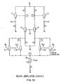
- a cell is selected for the READ operation when its row lines (WL, DL) and bit lines (BL, BR) are both selected ( Figure 12).
- the row lines are selected by the voltage mode word selection scheme as previously described.
- the bit lines are selected by the bit selection scheme explained earlier ( Figure 3).
- I L and I G are fed into its bit rail Schottky SL and SR, which then couple the cell's internal voltages ("0" and "1") on to the bit lines for READ sensing.
- I L and I G currents have to be controlled within a chosen operating range. This is accomplished by a READ reference level applied to the bit rail driving transistors (T 1 and T 2 of Figure 12) from the UC line.
- the READ reference is generated by a bit up level clamp circuit (Bit UPCL, Figure 7) which tracks fully with the selected cells, so that sufficient voltage potentials (V"O" and V"1") are always ensured across bit rail resistors RBL and RBR to define I L and I G currents.
- Bit up level clamp circuit Bit UPCL, Figure 7
- the magnitude of the DC WRITE current Iw is controlled by a WRITE reference level applied to the bit rail driving transistor Tl or T2 through the U c line. This WRITE current can readily be adjusted by changing the bit up level clamp's WRITE reference level.
- bit up level clamp circuit to define the selected cells' operating levels. This is particularly important for the READ operation.
- a read reference voltage is generated by the bit up level clamp to track with the selected cells in temperature, power supply (V N ) and device ( V BE and V FSBD ) variations, so that proper read currents (I G and I L ) are always guaranteed under all conditions to ensure cell stability.
- the bit up level clamp circuit ( Figure 7) represented in Figures 3 and 3A by the block labelled "BIT UPCL" will now be explained with particular reference to Figures 8, 12 and 13.
- the voltage level required at the emitter of the clamping diode T5 in READ mode can be determined by summing up the potential rises/falls from V N in the word decoder.
- the R/W control input of the bit up level clamp circuit ( Figure 7) is high.
- Transistor Tl is ON and T2 is OFF, so that node 3 is up to turn ON T3, T4 and T5.
- the output line UC is clamped down by T3 to generate a READ reference voltage defined by the equation below.
- V"1" is the voltage across the "1" side of the bit rail resistor. It is this voltage potential across RBL that defines the gate current I G to maintain cell stability during READ.
- V"1" is defined by the voltage difference between a V BE (forward mode Base-Emitter voltage of an NPN transistor) and V F (forward conduction voltage of a Schottky diode), it is therefore independent of power supply (Vp and V N ) variations.
- the R/W input is low.
- Transistor Tl is OFF and T2 is ON.
- Node 1 is high to pull up T6 while node 3 is down to shut OFF T3.
- the WRITE reference level at the UC line is given by:
- This WRITE reference voltage is applied to the bit rail driving transistors (T 1 and T 2 , Figure 13) to define the write current I W .
- sensing circuitry The operation of circuitry represented in Figure 3 by the block labelled “sensing circuitry" will now be explained with particular reference to Figures 10 and 11.
- FIG 3A illustrates the sensing scheme employed for the RAM shown in Figure 2.
- the 64 bit columns of this RAM are divided into four data groups of 16 bits.
- Each data group contains a sense amplifier ( Figure 10) .for READ sensing.
- the state of the sense amplifier is determined by the selected cell within its data group.
- Data read by the sense amplifier is sent off chip through an off chip driver (OCD) circuit.
- OCD off chip driver
- FIG 11 illustrates the sense amplifier arrangement for a data group.
- each bit column has a pair of sensing transistors (TL and TR) attached to its bit lines for voltage sensing.
- TL and TR sensing transistors
- Figure 10 illustrates a high speed sense amplifier circuit designed for the above sensing scheme.
- the circuit uses current steering technique to enable very fast switching performance. Its sensing speed is independent of the number of bit columns in the data group.
- the thirty-two sensing transistors T11 to TL16 and TR1 to TR16 form a big current switch input for the sense amplifier.
- the bases of these transistors are connected to the sixteen bit columns in the data group.
- Transistors Tl and T2 are emitter followers providing dual-phase outputs to drive the off chip driver.
- Transistors T3 and T4 are set to be ON all the time to define a fixed voltage at nodes A and B, so that switching of these two devices is done in current mode.
- bit-left or bit-right of a selected bit column is up at a high voltage level.
- the higher voltage bit line turns on its corresponding sensing transistor.
- the sense current IS from the current source T5 is then steered by the ON sensing transistor through either T3 or T4, pulling node 1 or 2 down accordingly.
Abstract
Description
- The invention is directed to an array of memory cells.
- Random access memories employing CTS type memory cells are known to the art. See for the example, the Gersbach patent 3,863,229, the Dorler et al IBM TDB publication "AC Write Scheme For Bipolar Random-Access Memories Using Schottky Coupled Cells", IBM TDB, Vol. 23, No. 11, April 1981, pages 4960-2, and the Dorler et al Article "A 1024 Byte ECL Random Access Memory Using a Complementary Transistor Switch (CTS) Cell", IBM Journal of Research and Development, Vol. 25, No. 3, May 1981, pages 126-34.
- The known random access memories and the in particular those employing CTS memory cells have two relatively serious bit selection short comings. First, the bit decode transistor has to drive a number of bit columns across the chip. Due to long metal line and large fan-out current, voltage drop along the bit decode line is high. The cells at the end of the bit decode line may have insufficient voltage across their "1" bit rail resistors to provide adequate gate currents into the cells. This may lead to potential data retention problems on the selected cells. Secondly, both selection and deselection of the bit rails are slow due to the fact that the bit decode transistor has large fan-out loadings. Discharge speed of the bit rails is limited by the bit rail resistors. The bit selection scheme in accordance with the invention obviates the above recited short comings of known RAMs and in particular RAMs using CTS cells.
- In high performance arrays using cells like CTS, selection of a cell is accomplished by lowering its word lines and raising its bit rails. Known designs use a fixed current source to pull down the selected word lines. There are three problems usually associated with this method of word- selection in "current mode".
- With CTS cells, the word lines are very capacitive. (For word lines having 60 to 80 cells, this word line capacitance could be as high as 30 to 40 pf). A constant current source pulls down the selected word lines according to its large RC time constant. Hence cell selection is very slow, and its drive capability is often limited by the fixed source of current.
- Since the selected word lines are held down by a current source, their voltage levels are easily affected by noise or current source variations. If the word line levels drift to a degree that they no longer track with those of the bit rails, data retention problems could result.
- During write operation, the bit line voltage of the side to be written a "1" is driven high. This causes the bit rail and the drain line levels to rise. A long address set up time is needed to wait for the previous selected cell to get out of the way before writing can start in order to avoid write-through problems.
- The above problems are obviated and overcome by the "voltage mode word selection scheme" in accordance with the invention.
- The object of the invention is to provide an improved random access memory which employs complementary transistor switch (CTS) memory cells, which obviates data retention concerns on fully selected cells, and improves (1) speed of selection of word lines, (2) stability of selected word lines, and (3) reduces address set-up time for "write" operation.
- The solution of the object is characterized in
claim 1. The bit select circuitry includes interconnected first and second level matrix decoders, each memory column has a pair of bit lines, each pair of bit lines has connected thereto bit select circuit means, each of said bit select circuit means being connected to an output of said second level decoder, a bit up level clamp circuit connected to each of said bit select circuit means of each pair of bit lines, each of said bit select circuit means including first circuit means for increasing the speed of selection of the selected pair of bit lines, said bit up level clamp circuit cooperating with said bit select circuit means of said selected pair of bit lines for positively limiting the upper potential level of said selected pair of bit lines, and each of said bit select circuit means including second circuit means for increasing the speed of deselection of the selected pair of bit lines. The invention also includes voltage mode word selection means in a RAM preferably employing CTS type memory cells. - The foregoing and other objects, features and advantages of the invention will be apparent from the following more particular description of preferred embodiments of the invention, as illustrated in the accompanying drawings.
-
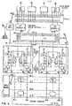
- Figure 1 illustrates bit select and word select circuitry in accordance with known RAMs employing CTS memory cells.
- Figure 1A illustrates the circuit of a known "unclamped" CTS memory cell.
- Figure 2 illustrates a lk x 4 random access memory in accordance with the invention.
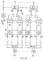
- Figure 3 illustrates the bit path circuitry of the random access memory shown in Figure 2.
- Figure 3A (to be reviewed in conjunction with Figure 3) illustrates the sensing and write control circuitry of the random access memory in accordance with Figure 3 and with the invention.
- Figure 4 is a circuit diagram of the address receiver circuits (Bit REC and Word REC) which may be employed in a RAM (Figure 3) in accordance with the invention.
- Figure 5 is a circuit diagram of a bit decoder circuit which may be employed in a RAM (Figure 3) in accordance with the invention.
- Figure 6 is a circuit diagram of a bit select circuit which may be employed in a RAM (Figure 3) in accordance with the invention.
- Figure 7 is a circuit diagram of the bit up-level clamp (Bit UPCL) which may be employed in a RAM (Figure 3) in accordance with the invention.
- Figure 8 illustrates the circuit diagram of "voltage mode" word selection scheme which may be employed in a RAM (Figure 3) in accordance with the invention.
- Figure 9 illustrates the circuit diagram of the word decoder circuit in accordance with Figure 8 and with the invention.
- Figure 10 illustrates the circuitry of a sense amplifier which may be employed in a RAM (Figure 3) in accordance with the invention.
- Figure 11 is a rearrangement of, and further illustrates the senses amplifier circuitry of Figure 10.
- Figure 12 is a further diagram referred to hereinafter in the explanation of the voltage mode READ operation of the RAM (Figures 3 & 8) in accordance with the invention.
- Figure 13 is a further-diagram referred to herein-after in the explanation of the voltage mode WRITE operation of the RAM in accordance with the invention.
- Figure 14 discloses idealized wave forms of the "WRITE" operation timing. Figure 14 is to be viewed in conjunction with the explanation of the WRITE operation (Figure 13) of the RAM (Figure 3) in accordance with the invention.
- In high performance arrays using CTS cells, selection of a cell is done by lowering its word lines and raising its bit rails. As depicted in Figure 1, known designs use a fi::ed current source to pull down the selected word and drain lines. There are three problems frequently associated with the "current mode" method of word selection.
- With CTS cells, the word lines are very capacitive. (For word lines having 60 to 80 cells, this word line capacitance could be as high as 30 to 40 pf). A constant current source pulls down the selected word line according to its large RC time constant. Hence, cell selection is very slow, and its drive capability is often limited by the fixed source of current.
- Since the selected word lines are held down by a current source, their voltage levels are easily affected by noise or current variations. If the word line levels drift to a degree that they no longer track with those of the bit rails, data retention problems could result.
- During write operation, the bit line voltage of the side to be written a "1" is driven high. This causes the bit rail and the drain line levels to rise. A long address set up time is needed to wait for the previous selected cell to go out of the way before writing can start in order to avoid write-through problems.
- The above problems are overcome and obviated by the "voltage mode word selection technique" in accordance with the invention and as disclosed herein. Figure 8 shows the schematic diagram of this scheme.
- Also known high performance arrays using CTS cells have bit selection concerns or short comings. Again referring to Figure 1, these concerns are as follows:
- 1. The bit decode transistor TB has to drive a number of bit columns across the chip. Due to long metal line and large fan-out current, voltage drop along the bit decode line (BD) is high. The cells at the end of the bit decode line may have insufficient voltage potential across their "1" bit rail resistors to define adequate gate currents (Il) into the cells. This may lead to potential data retention problems on the selected cells.
- 2. Both selection and deselection of the bit rails are slow, due to the fact that the bit decode transistor has large fan-out loadings. Discharge speed of the bit rails is limited by the bit rail resistors RBL and RBR.
- The above problems and concerns are addressed and overcome by the random access memory disclosed hereinafter.
- The above problems are overcome by using distributive bit select circuits and word line selection circuits illustrated in Figures 3, 3A, 8 and 9.
- For purpose of illustration, Figure 2 shows a lk x 4 RAM in accordance with the invention. This RAM has an array density of 4096 cells arranged in 64 words (rows) by 64 bit (columns). The 64 bit columns are further divided into 4 data groups, so that it will write 4 bits (therefore 4 data inputs) and read 4 bits (4 data outputs) at a time. The RAM has 6 word addresses (to select 1 out of 64 rows) and 4 bit addresses (to select 4 out of 64 bits). Read and write operations are controlled by the RW input.
- Referring to Figure 3, a two level matrix decode scheme is employed for bit address decoding. The first level decode includes two groups of 4 address lines (BAO - BA3 and BA4 - BA7) formed from output emitter dotting of the four bit address receivers. The bit address receivers are current switch emitter follower circuits as shown in Figure 4. They convert the address inputs to true and complement signals. By means of emitter follower output dotting of the address receiver pairs, a partial decode of 1 out of 4 is formed from each group, hence, giving a total of two selected (low level) lines.
- The second level decode function is performed by the 16 bit decoders (Figure 5), which have current switch inputs and high speed push-pull outputs.
Input 1 of the bit decoder is connected to one of the 4 lines in BAO - BA3 address group, andinput 2 is connected to one in the BA4 - BA7 group. Of the 16 BD output lines, only one is decoded to a selected up level. Each BD line fans out to drive four bit columns (one from each data group), so that four cells are selected at a time for READ or WRITE operation. - Each bit column has a bit select circuit (Figures 3 and 6) to perform bit line select and deselect functions. The selected bit lines up level is set by a bit up level clamp circuit (Bit UPCL, Figure 7), so that the cells' read and write operating points can be readily adjusted by changing the up clamp (UC) level.
- For unclamped CTS cell, the SCR device operates in saturation mode. The cell, is more capacitive (due to higher B-C junction saturation capacitance) than a normal CTS with Schottky clamp. This makes the unclamped cell very difficult to write. It is essential that the bit select circuit is capable of driving high transient current into the cell to enable fast write performance. A novel circuit technique utilizing capacitive boot strapping and transient drive mechanism is designed for this application. The bit select circuit's modes of operation are described below.
- In an unselected state, the BD line is held low by its corresponding bit decoder to a voltage close to VN. Transistors T1 and T2 of the bit select circuit are driven into inverse saturated mode operation.
Nodes Nodes nodes nodes boot strap nodes nodes - When a bit column is selected, its BD line is actively pulled up by the corresponding bit decoder to a voltage about a VBE below Vp. This forces the collectors of Tl and T2 to move up quickly at the same rate. The rapid discharge of the B-C and B-E junctions of T1 and T2 provide very fast capacitive push up action on
nodes nodes nodes - During READ mode, both the PDL and PDR lines are high (up at around Vp).
Nodes - In the selected state, Tl and T2 operate in active forward mode to provide DC read currents. Transistors T3 and T4 are only turned ON transiently. They will stay OFF after the bit lines BL and BR reach their fully selected up levels. Since the BD line's voltage level is set to be higher than those of
nodes - In the WRITE mode, bit line selection is similar to that of the READ as described above. The only difference here is that one of the write control lines (either PDL or PDR, depending on the data to be written) is driven negative to a voltage close to VN . by the write control circuit prior to bit selection (see Figure 13). The lowered PDL or PDR line will clamp down either
node - During WRITE mode,
node - When a bit column is deselected, its corresponding bit decoder output falls to the unselected down level. Transistors T1 and T2 of the bit select circuit are driven into inverse saturation mode.
Nodes - The disclosed bit select scheme has particular utility in arrays using CTS (Complementary Transistor Switch, Figure lA) cells. With this scheme, at least the following two advantages have been achieved over the known designs.
-
- (I) Improved bit line "select/deselect" speed, hence faster bit path access time.
- (II) Eliminates the effects of bit decode up level line drop, hence reduce data retention concerns for the selected cells.
- The improved bit selection circuit means, in accordance with the invention includes the following elements:
- 1. Two level matrix decode (Figure 3) - First level is emitter dotting of the current switch emitter follower address receivers. Second level is the bit decoders with current switch input and high speed push-pull outputs.
- 2. Distributive bit select circuit (Figures 3 & 6). It utilizes capacitive discharge mechanism of inverse saturation transistors (Tl & T2) to enhance bit rail selection speed. The same transistors are also used in active forward mode (when the bit column is selected) to source the DC READ and WRITE currents into the cell through resistors RBL and RBR. It has transistors T3 and T4 to provide high speed high power transient drive mechanism on the bit lines to enable fast READ/WRITE performance. It uses Schottky barrier diodes (SL and SR) in conjunction with the bit rail resistors RBL & RBR for active bit rail pull down to enable fast bit column deselection. It also uses multi-emitter transistor diodes T5 and T6 for READ/WRITE control as well as setting the operating points for the selected cell.
- 3. Bit up level clamp (Figures 3 and 7) - The selected bit lines' read and write up levels are controlled by a reference circuit (Bit UPCL) so as to enable easy operating point adjustment. This circuit is also designed, as more fully explained hereinafter, to meet various tracking requirements (such as tracking with selected drain line level in read mode).
- The improved word line decoder and control circuitry represented by the block labelled "Word Decode" in Figure 3 is shown in detail in Figures 8 and 9. Figure 8 shows the voltage mode word selection scheme whereas Figure 9 discloses in detail the circuit of the word decoder.
- Referring to Figure 8, there are 6 word addresses to decode 1 out of 64 rows. A two level matrix decode scheme similar to that of the bit path is employed for word address decoding. The first level decode includes three groups of 4 address lines (WA4 -.WA3, WAO - WA7, and WA8 - WA11) formed from output emitter dotting of the 6 word address receivers. The word address receivers are current switch emitter follower circuits (Figure 4). They convert the address inputs to true and complement signals. By means of emitter follower output dotting of the address receiver pairs, a partial decode of 1 out of 4 is obtained from each group, hence giving a total of three selected (low level) lines.
- The second level decode function is performed by the 64 word decoders (Figure 9). Each word decoder has three current switch inputs (IN1 - IN3) and two high speed high power push-pull outputs (WL and DL). IN1 of the word decoder is connected to one of the four lines in WAO - WA3 address group. IN2 is connected to one in the second group (WA4 - WA7), and IN3 is connected to one in the third group (WA8 - WAll). All these three inputs have to be low in order to select a row line. The two outputs of the word decoder are connected to the word line (WL) and drain line (DL) of the memory cells as shown.
- Operations of the word decoder, in accordance with the invention, are explained hereinafter.
- An unselected word decoder will have at least one of its three inputs high. Decoding transistors T1, T2 or T3 are turned ON to pull down
node 1. Transistors T5 and T6 form a dual phase level shifter, so thatnode 4 is also pulled negative to a voltage close to VN andnode 3 is pulled positive to Vp. Withnode 4 being down, the open collector transistor TL is shut off, allowing the word line WL and drain line DL to move up to their unselected (high) levels. In this state, the cells' stand-by current, as well as word and drain line voltages are defined by the current sources ISBH and ISBL. - To enable fast switching speed, transistors T5 and T6 are never shut OFF but kept in slight conduction. The active pull up devices (T7 and TH) are OFF when the word line reaches its full unselected DC level (about one and a half VBE below Vp).
- When a word decoder is selected, all its three inputs are low. Transistors Tl, T2 and T3 are OFF.
Node 1 goes high to turn ON T5 and T6 hard.Node 3 is pulled down by T5's collector to keep T7 - T OFF, so that WL and DL are allowed to move down to their selected levels. At the same time,node 4 is driven high to turn ON TL. It is this high power open collector pull down action on the drain line that enables the cells to be selected fast. While the drain line is being driven low, the word line follows it at the same rate with a voltage offset defined by the cells. - When the word and drain lines are fully selected, T7 - TH are OFF and TL is maintained ON to sink the large READ/WRITE currents conducting from the selected cells. In this state, the word and drain line voltages are defined by following two equations:


- Since the selected drain line is pulled down by a high power open collector transistor (TL), word selection is therefore very fast and its drive capability is not limited by fixed current sources as in prior designs. Furthermore, the selected drain and word line levels are solidly defined to voltages offset from power supply VN, they are more stable than those of the prior art. This technique of word selection is denoted herein as "Voltage Mode Word Selection".
- After a row line has been selected for a READ or a WRITE operation, it is deselected back to its stand-by state. A deselecting word deocder will have at least one of its inputs go positive. Decoding transistors Tl, T2 or T3 are turned ON again, driving
node 1 down to shut OFF the open collector transistor TZ. At the same time,node 4 is pulled positive to Vp, driving the emitter follower devices T7 - TH transiently ON to pull up word line WL until it reaches its unselected DC level. While the word line is being pulled positive, drain line DL follows it up at the same rate with a voltage offset defined by the cells. When the word and drain lines are fully up at their stand-by levels, T7 - TH and TL are all OFF. The row line is now said to be in an unselected state. - A cell is selected for the READ operation when its row lines (WL, DL) and bit lines (BL, BR) are both selected (Figure 12). The row lines are selected by the voltage mode word selection scheme as previously described. The bit lines are selected by the bit selection scheme explained earlier (Figure 3). After a cell is fully selected, read currents IL and IG are fed into its bit rail Schottky SL and SR, which then couple the cell's internal voltages ("0" and "1") on to the bit lines for READ sensing. In order to guarantee cell stability during READ, IL and IG currents have to be controlled within a chosen operating range. This is accomplished by a READ reference level applied to the bit rail driving transistors (T1 and T2 of Figure 12) from the UC line. The READ reference is generated by a bit up level clamp circuit (Bit UPCL, Figure 7) which tracks fully with the selected cells, so that sufficient voltage potentials (V"O" and V"1") are always ensured across bit rail resistors RBL and RBR to define IL and IG currents. Generation of this READ reference level, and the operation of the bit up level clamp circuit, will be more fully explained in the following sections.
- With voltage mode word selection technique, WRITE operation is performed in three sequential steps (Figures 13 and 14).
-
- 1. The row lines are selected/deselected as previously described.
- 2. After crossing of the selecting and deselecting drain lines (see Figure 14), WRITE operation is initiated. The RW clock switches the bit up level clamp circuit to generate a WRITE reference voltage on the UC line. This RW signal is also applied to a write control circuit, which depending on its data input, will drive either one of its two output lines PDL or PDR low. The lowered PDL or PDR line will then pull down
node - 3. After the PDL or PDR line is lowered, the bit select circuit is selected. The side of the bit line to be written a "1" is raised high by the bit rail driving transistors Tl-T3 or T2-T4. Large transient write current is injected into the cell through T3-RBL or T4-RBR until the desired cell state is reached. After the cell has been written, the bit line voltage of the "1" side will rise up to its normal "1" level. This reduces the potential difference across the conducting bit rail resistor RBL or RBR, hence the transient transistor T3 or T4 is shut off. The bit rail resistor RBL or RBR will then supply a small DC WRITE current (IW) from Tl or T2 to reinforce the state of the newly written cell.
- The magnitude of the DC WRITE current Iw is controlled by a WRITE reference level applied to the bit rail driving transistor Tl or T2 through the Uc line. This WRITE current can readily be adjusted by changing the bit up level clamp's WRITE reference level.
- The above write scheme is denoted "Differential Mode Write", since one side of the bit line is raised high while the other side is being held low during write time.
- The key advantage of this write scheme is that since the drain line is selected to a fixed voltage a VCE above VN, when write current is injected into the cell, the level of this line will not move up but remain stable. The chasing effect with the deselecting cells as exists in "current mode" word selection scheme used by prior art designs is hence eliminated. The RW clock can now come in sooner (as soon as the selecting and deselecting drain lines cross over) without waiting for the deselecting cells to get out of the way. This minimizes address set up time required prior to write. Due to faster word selection and shorter address set up time, write performance is therefore greatly improved. Furthermore, since the selected drain line is solidly held to a voltage level, and the deselected one is actively pulled up quickly to its unselected level, no "write through" (i.e., writing into the deselecting as well as the stand-by cells) problems exist.
- As is submitted to be evident from the above description the use of the voltage mode word selection technique, in accordance with the invention, particularly in CTS RAMs, provides the following benefit and advantages:
- (1) Enables very high speed word select and deselect, hence faster "READ" performance.
- (2) Provides large row lines drive capability, hence very desirable for high density applications.
- (3) Stabilizes the selected drain line level, hence eliminates possible data retention and WRITE through problems.
- (4) Enables faster "WRITE" performance.
- The proper operation of a voltage mode word selection scheme in a CTS RAM requires a bit up level clamp circuit to define the selected cells' operating levels. This is particularly important for the READ operation. A read reference voltage is generated by the bit up level clamp to track with the selected cells in temperature, power supply (VN) and device (V BE and V FSBD) variations, so that proper read currents (IG and IL) are always guaranteed under all conditions to ensure cell stability. The bit up level clamp circuit (Figure 7) represented in Figures 3 and 3A by the block labelled "BIT UPCL" will now be explained with particular reference to Figures 8, 12 and 13.
- Referring to Figure 12, the voltage level required at the emitter of the clamping diode T5 in READ mode can be determined by summing up the potential rises/falls from VN in the word decoder.

- Cancelling the VBE rises/falls and VF rises/falls in the above expression, a simplified equation defining the READ reference voltage is obtained:

- For a READ operation, the R/W control input of the bit up level clamp circuit (Figure 7) is high. Transistor Tl is ON and T2 is OFF, so that
node 3 is up to turn ON T3, T4 and T5. The output line UC is clamped down by T3 to generate a READ reference voltage defined by the equation below.
- Equating expressions (1) and (2), we have: Voltage @ T5 = VUC(READ)

- V"1" is the voltage across the "1" side of the bit rail resistor. It is this voltage potential across RBL that defines the gate current IG to maintain cell stability during READ. The read currents IG and IL are related by the following expressions:

and V"0" = V"1" + VF - As seen from equation (3), since V"1" is defined by the voltage difference between a VBE (forward mode Base-Emitter voltage of an NPN transistor) and VF (forward conduction voltage of a Schottky diode), it is therefore independent of power supply (Vp and VN) variations.
- Furthermore, temperture effects on the devices are also equally cancelled out.
- In a WRITE mode, the R/W input is low. Transistor Tl is OFF and T2 is ON.
Node 1 is high to pull up T6 whilenode 3 is down to shut OFF T3. The WRITE reference level at the UC line is given by:
- This WRITE reference voltage is applied to the bit rail driving transistors (T1 and T2, Figure 13) to define the write current IW.
- The operation of circuitry represented in Figure 3 by the block labelled "sensing circuitry" will now be explained with particular reference to Figures 10 and 11.
- Figure 3A illustrates the sensing scheme employed for the RAM shown in Figure 2. The 64 bit columns of this RAM are divided into four data groups of 16 bits. Each data group contains a sense amplifier (Figure 10) .for READ sensing. The state of the sense amplifier is determined by the selected cell within its data group. Data read by the sense amplifier is sent off chip through an off chip driver (OCD) circuit.
- Figure 11 illustrates the sense amplifier arrangement for a data group. Within a data group, each bit column has a pair of sensing transistors (TL and TR) attached to its bit lines for voltage sensing. When a cell is selected for READ, its row lines (WL and DL) are pulled down by its corresponding word decoder, and its bit lines (BL and BR) are raised up by its bit select circuit. Since there are 16 bit columns per data group, bit selection is always 1 out of 16. Of the thirty-two bit lines, only two are up at any one time. The higher of these two selected bit lines turns on the corresponding sensing transistor in the sense amplifier circuit.
- Figure 10 illustrates a high speed sense amplifier circuit designed for the above sensing scheme. The circuit uses current steering technique to enable very fast switching performance. Its sensing speed is independent of the number of bit columns in the data group.
- Referring to Figure 10, the thirty-two sensing transistors T11 to TL16 and TR1 to TR16 form a big current switch input for the sense amplifier. The bases of these transistors are connected to the sixteen bit columns in the data group. Transistors Tl and T2 are emitter followers providing dual-phase outputs to drive the off chip driver. Transistors T3 and T4 are set to be ON all the time to define a fixed voltage at nodes A and B, so that switching of these two devices is done in current mode.
- At any time, either bit-left or bit-right of a selected bit column is up at a high voltage level. The higher voltage bit line turns on its corresponding sensing transistor. The sense current IS from the current source T5 is then steered by the ON sensing transistor through either T3 or T4, pulling
node - Since voltage levels at node A and B will never be switched but remain fixed, any capacitance at these nodes, therefore will have no effect on the switching time. In fact, the circuit's delay will stay constant, disregarding the number of sensing transistors attached to its input stage. Furthermore, transistors Tl, T2 and T3, T4 are active all the time; hence, their switching delay is kept to a minimum.
- The features of the sense amplifier circuit in Figure 10 are summarized as follows:
- 1. The sensing transistors are configurated as a bit current switch, with their bases connected to bit lines within the data group. This forms the input stage of the sense amplifier.
- 2. The switching of the circuit is done in current mode, i.e., input voltages at A and B are fixed, and switching is performed by steering sense current Is through T3 or T4. This mode of operation enables very large fan-in capability, as well as high circuit speed independent of input loadings.
- 3. All switching devices (Tl, T2 and T3, T4) are kept active at all times to minimize circuit delay.
- It is to be appreciated, that for convenience of explanation and understanding, in the foregoing description of applicants' invention only a limited number of memory cells, word lines etc. were shown and described. Persons skilled in the art readily recognize that the size of the Array depicted in the drawing and described in the specification is not to be construed as a limitation on applicants' invention.
Claims (8)
characterized in that the second level of circuitry of said word line decoder circuit means includes n decoder circuits each of said n decoder circuits having at least one input and providing one of said n outputs.
Applications Claiming Priority (2)
| Application Number | Priority Date | Filing Date | Title |
|---|---|---|---|
| US06/624,489 US4598390A (en) | 1984-06-25 | 1984-06-25 | Random access memory RAM employing complementary transistor switch (CTS) memory cells |
| US624489 | 1984-06-25 |
Publications (3)
| Publication Number | Publication Date |
|---|---|
| EP0169360A2 true EP0169360A2 (en) | 1986-01-29 |
| EP0169360A3 EP0169360A3 (en) | 1989-02-08 |
| EP0169360B1 EP0169360B1 (en) | 1992-04-08 |
Family
ID=24502202
Family Applications (1)
| Application Number | Title | Priority Date | Filing Date |
|---|---|---|---|
| EP85107232A Expired EP0169360B1 (en) | 1984-06-25 | 1985-06-13 | Random access memory |
Country Status (4)
| Country | Link |
|---|---|
| US (1) | US4598390A (en) |
| EP (1) | EP0169360B1 (en) |
| JP (1) | JPS619894A (en) |
| DE (1) | DE3585811D1 (en) |
Cited By (1)
| Publication number | Priority date | Publication date | Assignee | Title |
|---|---|---|---|---|
| EP0247324A2 (en) * | 1986-04-30 | 1987-12-02 | International Business Machines Corporation | Improved random access memory employing complementary transistor switch (CTS) memory cells |
Families Citing this family (16)
| Publication number | Priority date | Publication date | Assignee | Title |
|---|---|---|---|---|
| JPS60254484A (en) * | 1984-05-31 | 1985-12-16 | Fujitsu Ltd | Semiconductor integrated circuit device |
| US4792923A (en) * | 1985-08-30 | 1988-12-20 | Mitsubishi Denki Kabushiki Kaisha | Bipolar semiconductor memory device with double word lines structure |
| US4922455A (en) * | 1987-09-08 | 1990-05-01 | International Business Machines Corporation | Memory cell with active device for saturation capacitance discharge prior to writing |
| JPH023187A (en) * | 1988-06-09 | 1990-01-08 | Toshiba Corp | Non-volatile semiconductor memory |
| DE69023456T2 (en) * | 1989-10-30 | 1996-06-20 | Ibm | Bit decoding scheme for memory arrays. |
| US5022010A (en) * | 1989-10-30 | 1991-06-04 | International Business Machines Corporation | Word decoder for a memory array |
| JPH0775734B2 (en) * | 1990-11-09 | 1995-08-16 | 川崎製鉄株式会社 | Straightening roll unit used for shaped steel roll straightening machine |
| US9564199B2 (en) | 2014-09-25 | 2017-02-07 | Kilopass Technology, Inc. | Methods of reading and writing data in a thyristor random access memory |
| US9460771B2 (en) * | 2014-09-25 | 2016-10-04 | Kilopass Technology, Inc. | Two-transistor thyristor SRAM circuit and methods of operation |
| US9613968B2 (en) | 2014-09-25 | 2017-04-04 | Kilopass Technology, Inc. | Cross-coupled thyristor SRAM semiconductor structures and methods of fabrication |
| US9496021B2 (en) * | 2014-09-25 | 2016-11-15 | Kilopass Technology, Inc. | Power reduction in thyristor random access memory |
| US9530482B2 (en) | 2014-09-25 | 2016-12-27 | Kilopass Technology, Inc. | Methods of retaining and refreshing data in a thyristor random access memory |
| US20160093624A1 (en) | 2014-09-25 | 2016-03-31 | Kilopass Technology, Inc. | Thyristor Volatile Random Access Memory and Methods of Manufacture |
| US9741413B2 (en) | 2014-09-25 | 2017-08-22 | Kilopass Technology, Inc. | Methods of reading six-transistor cross-coupled thyristor-based SRAM memory cells |
| US9449669B2 (en) | 2014-09-25 | 2016-09-20 | Kilopass Technology, Inc. | Cross-coupled thyristor SRAM circuits and methods of operation |
| US9564441B2 (en) | 2014-09-25 | 2017-02-07 | Kilopass Technology, Inc. | Two-transistor SRAM semiconductor structure and methods of fabrication |
Family Cites Families (34)
| Publication number | Priority date | Publication date | Assignee | Title |
|---|---|---|---|---|
| US3423737A (en) * | 1965-06-21 | 1969-01-21 | Ibm | Nondestructive read transistor memory cell |
| US3525084A (en) * | 1967-12-14 | 1970-08-18 | Ibm | Memory sense system with fast recovery |
| US3582911A (en) * | 1968-12-04 | 1971-06-01 | Ferroxcube Corp | Core memory selection matrix |
| US3753008A (en) * | 1970-06-20 | 1973-08-14 | Honeywell Inf Systems | Memory pre-driver circuit |
| US3623033A (en) * | 1970-06-29 | 1971-11-23 | Electronic Memories & Magnetic | Cross-coupled bridge core memory addressing system |
| US3636377A (en) * | 1970-07-21 | 1972-01-18 | Semi Conductor Electronic Memo | Bipolar semiconductor random access memory |
| US3736574A (en) * | 1971-12-30 | 1973-05-29 | Ibm | Pseudo-hierarchy memory system |
| US3786442A (en) * | 1972-02-24 | 1974-01-15 | Cogar Corp | Rapid recovery circuit for capacitively loaded bit lines |
| US3789243A (en) * | 1972-07-05 | 1974-01-29 | Ibm | Monolithic memory sense amplifier/bit driver having active bit/sense line pull-up |
| US3771147A (en) * | 1972-12-04 | 1973-11-06 | Bell Telephone Labor Inc | Igfet memory system |
| US3843954A (en) * | 1972-12-29 | 1974-10-22 | Ibm | High-voltage integrated driver circuit and memory embodying same |
| US3863229A (en) * | 1973-06-25 | 1975-01-28 | Ibm | Scr (or scs) memory array with internal and external load resistors |
| US3919566A (en) * | 1973-12-26 | 1975-11-11 | Motorola Inc | Sense-write circuit for bipolar integrated circuit ram |
| US3942160A (en) * | 1974-06-03 | 1976-03-02 | Motorola, Inc. | Bit sense line speed-up circuit for MOS RAM |
| FR2304991A1 (en) * | 1975-03-15 | 1976-10-15 | Ibm | ARRANGEMENT OF CIRCUITS FOR SEMICONDUCTOR MEMORY AND ITS OPERATING PROCEDURE |
| US4007451A (en) * | 1975-05-30 | 1977-02-08 | International Business Machines Corporation | Method and circuit arrangement for operating a highly integrated monolithic information store |
| US4078261A (en) * | 1976-01-02 | 1978-03-07 | Motorola, Inc. | Sense/write circuits for bipolar random access memory |
| US4090254A (en) * | 1976-03-01 | 1978-05-16 | International Business Machines Corporation | Charge injector transistor memory |
| US4042915A (en) * | 1976-04-15 | 1977-08-16 | National Semiconductor Corporation | MOS dynamic random access memory having an improved address decoder circuit |
| US4104735A (en) * | 1976-09-15 | 1978-08-01 | Siemens Aktiengesellschaft | Arrangement for addressing a MOS store |
| US4174541A (en) * | 1976-12-01 | 1979-11-13 | Raytheon Company | Bipolar monolithic integrated circuit memory with standby power enable |
| DE2738187C2 (en) * | 1977-08-24 | 1979-02-15 | Siemens Ag, 1000 Berlin Und 8000 Muenchen | Circuit arrangement for a plurality of memory cells arranged on a bipolar module with a control circuit for adapting the characteristic curves of the memory cells |
| US4194130A (en) * | 1977-11-21 | 1980-03-18 | Motorola, Inc. | Digital predecoding system |
| US4242605A (en) * | 1978-05-22 | 1980-12-30 | Motorola, Inc. | Transient array drive for bipolar ROM/PROM |
| US4172291A (en) * | 1978-08-07 | 1979-10-23 | Fairchild Camera And Instrument Corp. | Preset circuit for information storage devices |
| US4264828A (en) * | 1978-11-27 | 1981-04-28 | Intel Corporation | MOS Static decoding circuit |
| DE2926050C2 (en) * | 1979-06-28 | 1981-10-01 | Ibm Deutschland Gmbh, 7000 Stuttgart | Method and circuit arrangement for reading and / or writing an integrated semiconductor memory with memory cells using MTL technology |
| JPS5847792B2 (en) * | 1979-07-26 | 1983-10-25 | 富士通株式会社 | Bit line control circuit |
| US4308595A (en) * | 1979-12-19 | 1981-12-29 | International Business Machines Corporation | Array driver |
| US4287575A (en) * | 1979-12-28 | 1981-09-01 | International Business Machines Corporation | High speed high density, multi-port random access memory cell |
| US4323986A (en) * | 1980-06-30 | 1982-04-06 | International Business Machines Corporation | Electronic storage array having DC stable conductivity modulated storage cells |
| JPS5841596B2 (en) * | 1980-11-28 | 1983-09-13 | 富士通株式会社 | Static semiconductor memory device |
| US4413191A (en) * | 1981-05-05 | 1983-11-01 | International Business Machines Corporation | Array word line driver system |
| US4417159A (en) * | 1981-08-18 | 1983-11-22 | International Business Machines Corporation | Diode-transistor active pull up driver |
-
1984
- 1984-06-25 US US06/624,489 patent/US4598390A/en not_active Expired - Fee Related
-
1985
- 1985-03-08 JP JP60045015A patent/JPS619894A/en active Granted
- 1985-06-13 DE DE8585107232T patent/DE3585811D1/en not_active Expired - Fee Related
- 1985-06-13 EP EP85107232A patent/EP0169360B1/en not_active Expired
Non-Patent Citations (4)
| Title |
|---|
| IBM TECHNICAL DISCLOSURE BULLETIN, vol. 23, no. 3, August 1980, pages 1077-1078, New York, US; G.BOUDON et al.: "Fast data access in a CTS cell matrix memory" * |
| IBM TECHNICAL DISCLOSURE BULLETIN, vol. 25, no. 6, November 1982, pages 2746-2750, New York, US; F.C.WERNICKE: "Circuit concept for rapidly reading and writing semiconductor storages with diode-coupled cells" * |
| IEEE TWENTY-FOURTH IEEE COMPUTER SOCIETY INTERNATIONAL CONFERENCE, San Francisco, California, 22nd-25th February 1982, Digest of Papers, COMPCON 82, "High Technical in the Information Industry", pages 58-61, IEEE, Inc., New York, US; R.D.DUSSAULT et al.: "Novel circuit techniques for dense bipolar RAMS" * |
| IEEE TWENTY-SECOND COMPUTER SOCIETY INTERNATIONAL CONFERENCE, San Francisco, California, 23rd-26th February 1981, Digest of Papers, VLSI, COMPCON 81, "In the laboratory the office the factory the home", pages 120-124, IEEE, Inc., New York, US; J.STINEHELFER et al.: "Large ECL bipolar RAMS" * |
Cited By (2)
| Publication number | Priority date | Publication date | Assignee | Title |
|---|---|---|---|---|
| EP0247324A2 (en) * | 1986-04-30 | 1987-12-02 | International Business Machines Corporation | Improved random access memory employing complementary transistor switch (CTS) memory cells |
| EP0247324A3 (en) * | 1986-04-30 | 1990-10-10 | International Business Machines Corporation | Improved random access memory employing complementary transistor switch (cts) memory cells |
Also Published As
| Publication number | Publication date |
|---|---|
| JPH0355912B2 (en) | 1991-08-26 |
| EP0169360A3 (en) | 1989-02-08 |
| EP0169360B1 (en) | 1992-04-08 |
| US4598390A (en) | 1986-07-01 |
| JPS619894A (en) | 1986-01-17 |
| DE3585811D1 (en) | 1992-05-14 |
Similar Documents
| Publication | Publication Date | Title |
|---|---|---|
| EP0169360A2 (en) | Random access memory | |
| US5371713A (en) | Semiconductor integrated circuit | |
| EP0169355B1 (en) | Random access memory | |
| US5058067A (en) | Individual bit line recovery circuits | |
| EP0247324B1 (en) | Improved random access memory employing complementary transistor switch (cts) memory cells | |
| JPH05251670A (en) | Semiconductor device | |
| US4651302A (en) | Read only memory including an isolation network connected between the array of memory cells and the output sense amplifier whereby reading speed is enhanced | |
| EP0222154B1 (en) | Semiconductor memory device and array | |
| EP0168633B1 (en) | Array selection circuitry for a random access memory | |
| JPS6331879B2 (en) | ||
| EP0469834B1 (en) | A BICMOS logic circuit with self-boosting immunity and a method therefor | |
| US5199000A (en) | Semiconductor memory circuit having switched voltage supply for data bus lines | |
| JPH029087A (en) | Bi-cmos programming recovery circuit | |
| US4319344A (en) | Method and circuit arrangement for discharging bit line capacitances of an integrated semiconductor memory | |
| JPH0810556B2 (en) | Semiconductor memory circuit | |
| US4627034A (en) | Memory cell power scavenging apparatus and method | |
| US4070656A (en) | Read/write speed up circuit for integrated data memories | |
| US4697251A (en) | Bipolar RAM cell | |
| US5301148A (en) | Semiconductor memory device with bipolar-FET sense amp | |
| EP0185156B1 (en) | Random access memory | |
| US4899311A (en) | Clamping sense amplifier for bipolar ram | |
| US4701882A (en) | Bipolar RAM cell | |
| JPS6299976A (en) | Semiconductor memory device | |
| KR940005686B1 (en) | Sense amplifier of the dram | |
| JPH01155589A (en) | Semiconductor memory device |
Legal Events
| Date | Code | Title | Description |
|---|---|---|---|
| PUAI | Public reference made under article 153(3) epc to a published international application that has entered the european phase |
Free format text: ORIGINAL CODE: 0009012 |
|
| AK | Designated contracting states |
Designated state(s): DE FR GB |
|
| 17P | Request for examination filed |
Effective date: 19860424 |
|
| PUAL | Search report despatched |
Free format text: ORIGINAL CODE: 0009013 |
|
| AK | Designated contracting states |
Kind code of ref document: A3 Designated state(s): DE FR GB |
|
| 17Q | First examination report despatched |
Effective date: 19900516 |
|
| GRAA | (expected) grant |
Free format text: ORIGINAL CODE: 0009210 |
|
| AK | Designated contracting states |
Kind code of ref document: B1 Designated state(s): DE FR GB |
|
| PGFP | Annual fee paid to national office [announced via postgrant information from national office to epo] |
Ref country code: GB Payment date: 19920507 Year of fee payment: 8 |
|
| REF | Corresponds to: |
Ref document number: 3585811 Country of ref document: DE Date of ref document: 19920514 |
|
| PGFP | Annual fee paid to national office [announced via postgrant information from national office to epo] |
Ref country code: FR Payment date: 19920601 Year of fee payment: 8 |
|
| ET | Fr: translation filed | ||
| PGFP | Annual fee paid to national office [announced via postgrant information from national office to epo] |
Ref country code: DE Payment date: 19920619 Year of fee payment: 8 |
|
| PLBE | No opposition filed within time limit |
Free format text: ORIGINAL CODE: 0009261 |
|
| STAA | Information on the status of an ep patent application or granted ep patent |
Free format text: STATUS: NO OPPOSITION FILED WITHIN TIME LIMIT |
|
| 26N | No opposition filed | ||
| PG25 | Lapsed in a contracting state [announced via postgrant information from national office to epo] |
Ref country code: GB Effective date: 19930613 |
|
| GBPC | Gb: european patent ceased through non-payment of renewal fee |
Effective date: 19930613 |
|
| PG25 | Lapsed in a contracting state [announced via postgrant information from national office to epo] |
Ref country code: FR Effective date: 19940228 |
|
| PG25 | Lapsed in a contracting state [announced via postgrant information from national office to epo] |
Ref country code: DE Effective date: 19940301 |
|
| REG | Reference to a national code |
Ref country code: FR Ref legal event code: ST |