EP0167732A1 - Method for producing a basic material for a hybrid circuit - Google Patents
Method for producing a basic material for a hybrid circuit Download PDFInfo
- Publication number
- EP0167732A1 EP0167732A1 EP85104961A EP85104961A EP0167732A1 EP 0167732 A1 EP0167732 A1 EP 0167732A1 EP 85104961 A EP85104961 A EP 85104961A EP 85104961 A EP85104961 A EP 85104961A EP 0167732 A1 EP0167732 A1 EP 0167732A1
- Authority
- EP
- European Patent Office
- Prior art keywords
- conductor tracks
- metal layer
- contact points
- insulating layer
- substrate
- Prior art date
- Legal status (The legal status is an assumption and is not a legal conclusion. Google has not performed a legal analysis and makes no representation as to the accuracy of the status listed.)
- Granted
Links
Images
Classifications
-
- H—ELECTRICITY
- H01—ELECTRIC ELEMENTS
- H01L—SEMICONDUCTOR DEVICES NOT COVERED BY CLASS H10
- H01L23/00—Details of semiconductor or other solid state devices
- H01L23/52—Arrangements for conducting electric current within the device in operation from one component to another, i.e. interconnections, e.g. wires, lead frames
- H01L23/538—Arrangements for conducting electric current within the device in operation from one component to another, i.e. interconnections, e.g. wires, lead frames the interconnection structure between a plurality of semiconductor chips being formed on, or in, insulating substrates
- H01L23/5382—Adaptable interconnections, e.g. for engineering changes
-
- H—ELECTRICITY
- H01—ELECTRIC ELEMENTS
- H01L—SEMICONDUCTOR DEVICES NOT COVERED BY CLASS H10
- H01L21/00—Processes or apparatus adapted for the manufacture or treatment of semiconductor or solid state devices or of parts thereof
- H01L21/02—Manufacture or treatment of semiconductor devices or of parts thereof
- H01L21/04—Manufacture or treatment of semiconductor devices or of parts thereof the devices having at least one potential-jump barrier or surface barrier, e.g. PN junction, depletion layer or carrier concentration layer
- H01L21/48—Manufacture or treatment of parts, e.g. containers, prior to assembly of the devices, using processes not provided for in a single one of the subgroups H01L21/06 - H01L21/326
- H01L21/4814—Conductive parts
- H01L21/4846—Leads on or in insulating or insulated substrates, e.g. metallisation
-
- H—ELECTRICITY
- H01—ELECTRIC ELEMENTS
- H01L—SEMICONDUCTOR DEVICES NOT COVERED BY CLASS H10
- H01L2924/00—Indexing scheme for arrangements or methods for connecting or disconnecting semiconductor or solid-state bodies as covered by H01L24/00
- H01L2924/0001—Technical content checked by a classifier
- H01L2924/0002—Not covered by any one of groups H01L24/00, H01L24/00 and H01L2224/00
-
- H—ELECTRICITY
- H05—ELECTRIC TECHNIQUES NOT OTHERWISE PROVIDED FOR
- H05K—PRINTED CIRCUITS; CASINGS OR CONSTRUCTIONAL DETAILS OF ELECTRIC APPARATUS; MANUFACTURE OF ASSEMBLAGES OF ELECTRICAL COMPONENTS
- H05K1/00—Printed circuits
- H05K1/02—Details
- H05K1/0286—Programmable, customizable or modifiable circuits
Definitions
- the invention relates to a method for producing a base material for a hybrid circuit, consisting of a carrier substrate with multilayer metal layers which are electrically insulated from one another and can be subdivided in each case by suitable means into chip contact areas and conductor tracks.
- the invention is therefore based on the object of providing a hybrid base material which can be used universally and by means of which individual electrical circuits are possible in an economical manner, with minimal modifications, while maintaining the highest possible packing density.
- This object is achieved according to the invention in that the number of first conductor tracks formed from the one metal layer and the number of second conductor tracks formed from the other metal layer are specified at program-like contact points of the in different levels arranged and intersecting interconnects can be contacted with suitable means for forming an electrical circuit.
- the programmable hybrid substrate according to the invention can be produced using the methods and techniques known per se and stored as a base material, as a result of which the high one-off costs for circuit-specific design work and tools are eliminated. Another advantage is that this hybrid substrate ensures a high packing density and thus short connecting conductors, thereby permitting a high signal processing speed. Another advantage is seen in the fact that the programmability of the hybrid substrate enables a variety of circuits to be implemented which are almost copy-proof due to the always identical layout of the surface structure.
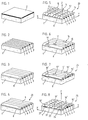
- FIG. 1, 1 denotes an electrically insulating substrate provided as a carrier element, on which a first metal layer 2 is vapor-deposited or sputtered.
- the metal layer 2 is etched in accordance with the photolithographic method of semiconductor technology known per se in such a way that, as shown in FIG. 2, a first group of conductor tracks 3, 4, 5, 6, 6 and 7 is formed parallel to one another.
- a first insulating layer shown in FIG. 3 and designated 8 is applied to the first conductor track group 3 to 7.
- This first insulating layer 8 serves as a protective layer electrically insulating the conductor tracks 3 to 7, to which, as shown in FIG. 4, a second metal layer 9 is applied.
- the second metal layer 9 is etched in such a way that a second group of conductor tracks 10, 11, 12 and 13 is arranged parallel to one another.
- the conductor tracks 10 to 13 are oriented essentially transversely to the conductor tracks 3 to 7 etched from the first metal layer 2.
- contact points K are formed which are electrically insulated from one another by the first insulating layer 8.
- FIG. 5 only one group of contact points K is designated for a better overview.
- the insulating layer 8 consists of polycrystalline, highly insulating silicon and the first and second metal layers 2, 9 for the upper and lower conductor tracks 3 to 7 and 10 to 13 consist of the aluminum usually used in semiconductor technology. Taking these features into account, there is the possibility of producing an electrically optimally conductive aluminum-silicon alloy by means of a focused laser beam by locally heating the contact points K to be contacted.
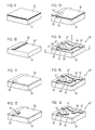
- any type of program is to be applied before the second metal layer is applied predetermined locations from the first insulating layer 8, as shown in more detail in FIG. 6, are etched out correspondingly designed windows 15, 16, 17 and 18.
- the second metal layer 9 ' is applied to the first insulating layer 8 provided with the windows 15 to 18, so that in the region of the windows 15 to 18 between the conductor tracks 3 to 7 and the second insulating layer 9' electrical contact points 15 'to 18' arise.
- the same is etched in such a way that, as shown in FIG.
- the carrier element (FIG. 3) formed from the essential elements 1 to 9 ' serves as the base material and is only after the relevant determination of the contact points 15' essentially formed by the windows 15 to 18. to 18 'and the production of a corresponding etching mask (not shown) for the hybrid substrate designated 25 in its entirety in FIG.
- the first metal layer 32 is etched such that, as shown in FIG. 10, at least one conductor track 33 is formed.
- a first insulating layer 34 (FIG. 11) is now applied to the conductor track 33 and to the surface 31 ′ of the substrate 31.
- At least one window 35 is etched from the insulating layer 34 (FIG. 12) and then, as shown in FIG. 13, a second one on the elements 31, 33, 34 and 35 Metal layer 36 applied. In this case, a contact point 35 ′ is formed in the area of the window 35 between the conductor track 33 and the second metal layer 36.
- the hybrid substrate designated 40 in its entirety in FIG. 14 serves as the prefabricated base material.
- the final state of the hybrid substrate, designated 40 'or 40 " is achieved in such a way that, for example, webs 39 which are not required and which essentially connect the conductor tracks 37 and 38 oriented parallel to one another, according to FIG. 15 by laser, or as shown in Fig. 16, interrupted by etching or removed.
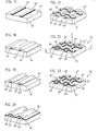
- the first metal layer 32 is etched in this example in such a way that, as shown in FIG. 17, two conductor tracks 33, 33 arranged parallel to one another 'arise.
- a subsequently applied first photoresist layer 44 (FIG. 18), as shown in FIG. 19, is subdivided into individual photoresist bridge parts 44 ′ that electrically isolate the two conductor tracks 33, 33 ′.
- a second metal layer 46 contacting the two bridge parts 44 'and the surface 31' is applied to the bridge parts 44 'and to the surface 31' of the substrate 31, which metal layer 46 is subsequently separated into individual Conductors 47, 48 oriented transversely to the conductor tracks 33, 33 'are subdivided (FIG. 21).
- the bridge parts 44 ′ formed from the photoresist layer 44 are removed by means of suitable means, so that, as shown in FIG. 22, a space 49, 49 ′ is created between the individual conductor tracks 33, 33 ′ and 47, 48.
- the hybrid substrate designated 50 in its entirety in FIG. 22 also serves as a prefabricated base material.
- the final state of the hybrid substrate 50 is essentially achieved by making an electrical contact at predetermined, programmed contact points K "of the intersecting conductor tracks 33, 33 'and 47, 48 and then an electrically insulating protective layer on the hybrid substrate 50 ( The interstices 49 and 49 'of the crossing conductor tracks 33, 33' and 47, 48 which are not designed as contact points K "are electrically insulated from one another.
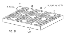
- FIG. 24 A perspective view of a larger section of the hybrid base material labeled 20, 25, 40, 40 ', 40 "and 50 is shown in FIG. 24 and the substrate 1 or 31 and the chip contact area labeled 60 can be seen.
- the one designated by a circle Position A corresponds to that here matically represented contact points K, K ', K "of the intersecting interconnects as described in more detail with reference to Examples I, II, III and IV.
- the hybrid base material 20, 25, 40, 40 ', 40 "and 50 according to the invention, described above and shown essentially as a partial section on a larger scale in FIGS. 1 to 24, can be produced by means of the already known and well-established techniques and processes.
Abstract
Description
Die Erfindung betrifft ein Verfahren zur Herstellung eines Basismaterials für eine Hybridschaltung, bestehend aus einem Trägersubstrat mit mehrlagig aufgebrachten, elektrisch gegeneinander isolierten und jeweils durch geeignete Mittel in Chip-Auflageflächen und Leiterbahnen unterteilbaren Metallschichten.The invention relates to a method for producing a base material for a hybrid circuit, consisting of a carrier substrate with multilayer metal layers which are electrically insulated from one another and can be subdivided in each case by suitable means into chip contact areas and conductor tracks.
Bekannte Verfahren zum Entwerfen und Herstellen von Hybridschaltungen erfordern eine aufwendige Entwicklung und auch eine kostenaufwendige, technische Realisierung. Dies ergibt sich insbesondere bei spezifischen Schaltungs-Anforderungen und aufgrund der Vielzahl unterschiedlicher Herstellungsschritte. Die bekannten Hybridbausteine eignen sich aus wirtschaftlichen Gründen ausschliesslich für relativ grosse Stückzahlen, wobei sie jedoch gegenüber den anderen, bekannten elektronischen Bausteinen den Vorteil einer hohen Packungsdichte und Zuverlässigkeit aufweisen.Known methods for designing and producing hybrid circuits require complex development and also costly, technical implementation. This is particularly the case with specific circuit requirements and due to the large number of different manufacturing steps. For economic reasons, the known hybrid modules are only suitable for relatively large quantities, but they have the advantage of a high packing density and reliability compared to the other known electronic modules.
Der Erfindung liegt deshalb die Aufgabe zugrunde ein universell verwendbares Hybrid-Basismaterial zu schaffen, mittels welchem unter Beibehaltung einer möglichst hohen Packungsdichte auf wirtschaftliche Weise, durch geringfügige Modifikationen, individuelle elektrische Schaltungen möglich sind.The invention is therefore based on the object of providing a hybrid base material which can be used universally and by means of which individual electrical circuits are possible in an economical manner, with minimal modifications, while maintaining the highest possible packing density.
Diese Aufgabe wird erfindungsgemäss dadurch gelöst, dass die aus der einen Metallschicht gebildete Anzahl erster Leiterbahnen mit der aus der anderen Metallschicht gebildeten Anzahl zweiter Leiterbahnen an programmartig vorbestimmten Kontaktstellen der in verschiedenen Ebenen angeordneten und sich kreuzenden Leiterbahnen mit geeigneten Mitteln zur Bildung einer elektrischen Schaltung durchkontaktiert werden.This object is achieved according to the invention in that the number of first conductor tracks formed from the one metal layer and the number of second conductor tracks formed from the other metal layer are specified at program-like contact points of the in different levels arranged and intersecting interconnects can be contacted with suitable means for forming an electrical circuit.
Das erfindungsgemässe, programmierbare Hybrid-Substrat kann unter Benutzung der an sich bekannten Verfahren und Techniken hergestellt und als Basismaterial gelagert werden, wodurch die hohen Einmalkosten für schaltungsspezifische Konstruktionsarbeiten und Werkzeuge entfallen. Ein weiterer Vorteil ist, dass dieses Hybrid-Substrat eine hohe Packungsdichte und somit kurze Verbindungsleiter gewährleistet und dadurch eine hohe Signalverarbeitungs-Geschwindigkeit zulässt. Als weiterer Vorteil wird angesehen, dass durch die Programmierbarkeit des Hybrid-Substrates mannigfaltige Schaltungen realisiert werden können, die aufgrund stets identischem Layout der Oberflächenstruktur nahezu kopiersicher sind.The programmable hybrid substrate according to the invention can be produced using the methods and techniques known per se and stored as a base material, as a result of which the high one-off costs for circuit-specific design work and tools are eliminated. Another advantage is that this hybrid substrate ensures a high packing density and thus short connecting conductors, thereby permitting a high signal processing speed. Another advantage is seen in the fact that the programmability of the hybrid substrate enables a variety of circuits to be implemented which are almost copy-proof due to the always identical layout of the surface structure.
Weiterbildungen der Erfindung ergeben sich aus der folgenden Beschreibung von Ausführungsbeispielen in Verbindung mit der Zeichnung und den Patentansprüchen. Es zeigt in vergrössertem Massstab
- Fig.1 ein perspektivisch in Schnittansicht dargestelltes Substrat-Teilstück mit einer ersten Metallschicht,
- Fig.2 das Substrat-Teilstück gemäss Fig.1 nach einem ersten Bearbeitungsschritt der ersten Metallschicht,
- Fig.3 das Substrat-Teilstück gemäss Fig.2 mit einer ersten Isolierschicht,
- Fi.4 das Substrat-Teilstück gemäss Fig.3 mit einer zweiten Metallschicht,
- Fig.5 ein erstes Beispiel eines Hybrid-Substrates, welches unter Verwendung des Substrat-Teilstückes gemäss Fig.1-4 hergestellt ist,
- Fig.6-8 ein zweites Beispiel eines Hybrid-Substrates, welches unter Verwendung des Substrat-Teilstückes gemäss Fig.1-4 hergestellt wurde,
- Fig.9-13 ein weiteres, in verschiedenen Stadien dargestelltes Substrat-Teilstück,
- Fig.14-16 ein drittes Beispiel eines Hybrid-Substrates, welches unter Verwendung des Substrat-Teilstückes gemäss Fig.9-13 hergestellt ist,
- Fig.17-20 ein weiteres, in verschiedenen Stadien dargestelltes Substrat-Teilstück,
- Fig.21-23 ein viertes Beispiel eines Hybrid-Substrates, welches unter Verwendung des Substrat-Teilstückes gemäss Fig.14-16 hergestellt ist,
- Fig.24 eine Perspektive des Basismaterials für eine Hybridschaltung mit den schematisch dargestellten Kontaktstellen und Chip-Auflageflächen.
- 1 shows a perspective section view of a substrate section with a first metal layer,
- 2 shows the substrate section according to FIG. 1 after a first processing step of the first metal layer,
- 3 shows the substrate section according to FIG. 2 with a first insulating layer,
- 4 shows the substrate section according to FIG. 3 with a second metal layer,
- 5 shows a first example of a hybrid substrate which is produced using the substrate section according to FIGS. 1-4,
- 6-8 shows a second example of a hybrid substrate which was produced using the substrate section according to FIG. 1-4,
- 9-13 a further substrate section shown in different stages,
- 14-16 a third example of a hybrid substrate, which is produced using the substrate section according to FIG. 9-13,
- Fig. 17-20 another substrate section shown in different stages,
- 21-23 a fourth example of a hybrid substrate which is produced using the substrate section according to FIGS. 14-16,
- 24 shows a perspective of the base material for a hybrid circuit with the schematically illustrated contact points and chip contact surfaces.
In Fig.1 ist mit 1 ein elektrisch isolierendes und als Trägerelement vorgesehenes Substrat bezeichnet, auf welchem eine erste Metallschicht 2 aufgedampft oder aufgestäubt ist. Die Metallschicht 2 wird nach dem an sich bekannten photolitographischen Verfahren der Halbleitertechnik derart geätzt, dass, wie in Fig.2 dargestellt, eine erste Gruppe parallel zueinander angeordnete Leiterbahnen 3,4,5,6, und 7 entsteht. Auf die erste Leiterbahnen-Gruppe 3 bis 7 wird eine in Fig.3 dargestellte und mit 8 bezeichnete erste Isolierschicht aufgebracht. Diese erste Isolierschicht 8 dient als eine die Leiterbahnen 3 bis 7 elektrisch isolierende Schutzschicht, auf welche, wie in Fig.4 dargestellt, eine zweite Metallschicht 9 aufgebracht ist.In FIG. 1, 1 denotes an electrically insulating substrate provided as a carrier element, on which a
Schaltungsbeispiele von dem in den Figuren 1,2,3 und 4 dargestellten und im wesentlichen aus den Elementen 1 bis 9 gebildeten und in den Figuren 4 und 5 in seiner Gesamtheit mit 20 bezeichneten Hybrid-Substrat werden nachstehend beschrieben.Circuit examples of the hybrid substrate shown in FIGS. 1, 2, 3 and 4 and essentially formed from
Hierbei wird, wie in Fig.5 dargestellt, die zweite Metallschicht 9 derart geätzt, dass eine zweite Gruppe parallel zueinander angeordneter Leiterbahnen 10,11,12 und 13 entsteht. Die Leiterbahnen 10 bis 13 sind im wesentlichen quer zu den aus der ersten Metallschicht 2 geätzten Leiterbahnen 3 bis 7 orientiert. In der flächigen Projektion der kreuzweise übereinander liegenden und entsprechend geätzten Leiterbahnen 3 bis 7 und 10 bis 13 entstehen Kontaktstellen K, die durch die erste Isolierschicht 8 voneinander elektrisch isolierend getrennt sind. In Fig.5 ist zur besseren Uebersicht nur eine Gruppe der Kontaktstellen K bezeichnet. Bei dem Ausführungsbeispiel gemäss Fig.5 besteht die Isolierschicht 8 aus polykristallinem, hochisolierendem Silizium und die erste und zweite Metallschicht 2,9 für die oberen und unteren Leiterbahnen 3 bis 7 sowie 10 bis 13 aus dem in der Halbleitertechnik üblicherweise verwendetem Aluminium. Unter Berücksichtigung dieser Merkmale besteht hierbei die Möglichkeit mittels eines fokussierten Laserstrahls durch lokale Erhitzung der zu kontaktierenden Kontaktstellen K eine elektrisch optimal leitende Aluminium-Silizium-Legierung zu erzeugen.In this case, as shown in FIG. 5, the
Ausgehend von dem in Fig.3 dargestellten und aus den Elementen 1 bis 8 gebildeten Hybrid-Substrat werden vor dem Aufbringen der zweiten Metallschicht an beliebig, programmartig vorbestimmten Stellen aus der ersten Isolierschicht 8, wie in Fig.6 näher dargestellt, entsprechend ausgebildete Fenster 15,16,17 und 18 ausgeätzt. Auf die mit den Fenstern 15 bis 18 versehene erste Isolierschicht 8 wird nunmehr, wie in Fig.7 dargestellt, die zweite Metallschicht 9' aufgebracht, so dass im Bereich der Fenster 15 bis 18 zwischen den Leiterbahnen 3 bis 7 und der zweiten Isolierschicht 9' elektrische Kontaktstellen 15' bis 18' entstehen. Nach dem Aufbringen der zweiten Metallschicht 9' wird dieselbe derart geätzt, dass, wie in Fig.8 dargestellt, quer zu den ersten Leiterbahnen 3 bis 7 orientierte, elektrisch isoliert voneinander getrennte Leiterbahnen 21,22,23 und 24 entstehen.Starting from the hybrid substrate shown in FIG. 3 and formed from
Bei dem Beispiel II gemäss den Figuren 6,7 und 8 dient das aus den wesentlichen Elementen 1 bis 9' gebildete Trägerelement (Fig.3) als Basismaterial und wird erst nach sachbezogener Festlegung der im wesentlichen mittels der Fenster 15 bis 18 gebildeten Kontaktstellen 15' bis 18' sowie der Herstellung einer entsprechenden Aetzmaske (nicht dargestellt) zu dem in Fig.7,8 in seiner Gesamtheit mit 25 bezeichneten Hybrid-Substrat verarbeitet.In the example II according to FIGS. 6, 7 and 8, the carrier element (FIG. 3) formed from the
Bei diesem Beispiel wird ausgehend von einem mit einer ersten Metallschicht 32 versehenen Substrat 31 (Fig.9) die erste Metallschicht 32 derart geätzt, dass, wie in Fig.10 dargestellt, mindestens eine Leiterbahn 33 entsteht. Auf die Leiterbahn 33 sowie auf die Fläche 31' des Substrats 31 wird nunmehr eine erste Isolierschicht 34 (Fig.11) aufgebracht. Aus der Isolierschicht 34 wird mindestens ein Fenster 35 geätzt (Fig.12) und anschliessend, wie in Fig.13 dargestellt, auf die Elemente 31,33,34 und 35 eine zweite Metallschicht 36 aufgebracht. Hierbei wird im Bereich des Fensters 35 zwischen der Leiterbahn 33 und der zweiten Metallschicht 36 eine Kontaktstelle 35' gebildet. Nach dem Aufbringen der zweiten Metallschicht 36 wird dieselbe derart geätzt, dass quer zu der ersten Leiterbahn 33 orientierte und, wie in Fig.14 dargestellt, durch einen Steg 39 miteinander in Verbindung stehende Leiterbahnen 37 und 38 entstehen. Die von der ersten Leiterbahn 33 und von den zweiten Leiterbahnen 37 und 38 gebildeten und durch die erste Isolierschicht 34 elektrisch isolierend voneinander getrennten Kontaktstellen K' werden anschliessend als elektrische Verbindungen durchkontaktiert.
Bei dem vorstehend beschriebenen Beispiel III dient das in Fig.14 in seiner Gesamtheit mit 40 bezeichnete Hybrid-Substrat als vorgefertigtes Basismaterial. Der Endzustand des mit 40' beziehungsweise mit 40" bezeichneten Hybrid-Substrates wird hierbei in der Weise erreicht, dass beispielsweise nichtbenötigte, die im wesentlichen die parallel zueinander orientierten Leiterbahnen 37 und 38 verbindenden Stege 39, gemäss Fig.15 durch Laser, oder aber, wie in Fig.16 dargestellt, durch Aetzen unterbrochen oder entfernt werden.In this example, starting from a substrate 31 (FIG. 9) provided with a
In Example III described above, the hybrid substrate designated 40 in its entirety in FIG. 14 serves as the prefabricated base material. The final state of the hybrid substrate, designated 40 'or 40 ", is achieved in such a way that, for example,
Ausgehend von dem in Fig.9 dargestellten und im wesentlichen aus dem Substrat 31 und der ersten Metallschicht 32 gebildeten Trägerelement wird bei diesem Beispiel die erste Metallschicht 32 derart geätzt, dass, wie in Fig.17 dargestellt, zwei parallel zueinander angeordnete Leiterbahnen 33,33' entstehen. Eine anschliessend aufgebrachte erste Fotolackschicht 44 (Fig.18) wird, wie in Fig.19 dargestellt, in einzelne, die beiden Leiterbahnen 33,33' elektrisch isolierende Fotolack-Brückenteile 44' unterteilt. Auf die Brückenteile 44' sowie auf die Fläche 31' des Substrates 31 wird, wie in Fig.20 dargestellt, eine zweite, die beiden Brückenteile 44' sowie die Fläche 31' kontaktierende Metallschicht 46 aufgebracht, welche Metallschicht 46 anschliessend durch eine entsprechende Aetzung in einzelne, quer zu den Leiterbahnen 33,33' orientierte Leiterbahnen 47, 48 unterteilt (Fig.21) wird. Mittels geeigneter Mittel werden die aus der Fotolackschicht 44 gebildeten Brückenteile 44' entfernt, so dass, wie in Fig.22 dargestellt, zwischen den einzelnen Leiterbahnen 33,33' sowie 47,48 jeweils ein Zwischenraum 49,49' entsteht.Starting from the carrier element shown in FIG. 9 and essentially formed from the
Bei dem vorstehend beschriebenen Beispiel IV dient das in Fig.22 in seiner Gesamtheit mit 50 bezeichnete Hybrid-Substrat ebenfalls als vorgefertigtes Basismaterial. Der Endzustand des Hybrid-Substrates 50 wird im wesentlichen dadurch erreicht, dass an vorbestimmten, programmierten Kontaktstellen K" der sich kreuzenden Leiterbahnen 33,33' und 47,48 ein elektrischer Kontakt hergestellt und anschliessend auf das Hybrid-Substrat 50 eine elektrisch isolierende Schutzschicht (nicht dargestellt) aufgebracht wird. Hierbei werden die nicht als Kontaktstellen K" ausgebildeten Zwischenräume 49 und 49' der sich kreuzenden Leiterbahnen 33, 33' sowie 47,48 elektrisch gegeneinander isoliert. Die Kontaktstellen K" werden vorzugsweise durch eine Ultraschall-Schweissung hergestellt und die Zwischenräume 49,49' mit geeignetem Quarz aufgefüllt.In example IV described above, the hybrid substrate designated 50 in its entirety in FIG. 22 also serves as a prefabricated base material. The final state of the
In Fig.24 ist perspektivisch ein grösseres Teilstück des mit 20,25,40,40',40"und 50 bezeichneten Hybrid-Basismaterials dargestellt und man erkennt das Substrat 1 beziehungsweise 31 sowie mit 60 bezeichnete Chip-Auflageflächen. Die durch einen Kreis bezeichnete Stelle A entspricht den hier schematisch dargestellten Kontaktstellen K,K',K" der sich kreuzenden Leiterbahnen wie sie anhand der Beispiele I,II,III und IV näher beschrieben sind.A perspective view of a larger section of the hybrid base material labeled 20, 25, 40, 40 ', 40 "and 50 is shown in FIG. 24 and the
Das erfindungsgemässe, vorstehend beschriebene und in den Figuren 1 bis 24 im wesentlichen als Teilstück in grösserem Massstab dargestellte Hybrid-Basismaterial 20,25,40,40',40" und 50 kann mittels der bereits bekannten und gut eingeführten Techniken und Verfahren hergestellt werden. Mit den in X- und Y-Richtung im wesentlichen quer zueinander und in Z-Richtung, wie in den Figuren 5,8,14 und 22 dargestellt, übereinanderliegend angeordneten Leiterbahnen 3 bis 7; 10 bis 13; 21 bis 24; 33,37 bis 39; 33,33' und 47,48 können bei einer Leiterbahnbreite sowie bei einem Leiterbahnabstand von 25 µ und bei einem 25mm x 25mm grossen Hybrid-Basismaterial annähernd 184.000 Kontaktierungsstellen hergestellt und dadurch schaltungstechnisch eine halbe, an sich bekannte Europaform-Karte integriert werden. Die Packungsdichte gegenüber der bekannten, konventionellen Leiterplattentechnik erhöht sich somit um einige Faktoren.The
Claims (7)
Priority Applications (1)
| Application Number | Priority Date | Filing Date | Title |
|---|---|---|---|
| AT85104961T ATE56310T1 (en) | 1984-06-27 | 1985-04-24 | PROCESS FOR MAKING A BASE MATERIAL FOR A HYBRID CIRCUIT. |
Applications Claiming Priority (2)
| Application Number | Priority Date | Filing Date | Title |
|---|---|---|---|
| CH310484 | 1984-06-27 | ||
| CH3104/84 | 1984-06-27 |
Publications (2)
| Publication Number | Publication Date |
|---|---|
| EP0167732A1 true EP0167732A1 (en) | 1986-01-15 |
| EP0167732B1 EP0167732B1 (en) | 1990-09-05 |
Family
ID=4248699
Family Applications (1)
| Application Number | Title | Priority Date | Filing Date |
|---|---|---|---|
| EP85104961A Expired - Lifetime EP0167732B1 (en) | 1984-06-27 | 1985-04-24 | Method for producing a basic material for a hybrid circuit |
Country Status (3)
| Country | Link |
|---|---|
| EP (1) | EP0167732B1 (en) |
| AT (1) | ATE56310T1 (en) |
| DE (1) | DE3579515D1 (en) |
Cited By (12)
| Publication number | Priority date | Publication date | Assignee | Title |
|---|---|---|---|---|
| EP0231970A2 (en) * | 1986-01-31 | 1987-08-12 | Philips Patentverwaltung GmbH | Thick-film wiring on a ceramic substrate plate |
| EP0256494A2 (en) * | 1986-08-12 | 1988-02-24 | Fujitsu Limited | Activatable conductive links for semiconductor devices |
| EP0268971A2 (en) * | 1986-11-24 | 1988-06-01 | Microelectronics and Computer Technology Corporation | Electrical interconnect support system with low dielectric constant |
| EP0329018A2 (en) * | 1988-02-19 | 1989-08-23 | Microelectronics and Computer Technology Corporation | Customizable circuitry |
| FR2653595A1 (en) * | 1989-10-25 | 1991-04-26 | Valtronic France | Electronic circuit inter-connection grid |
| US5074037A (en) * | 1989-12-01 | 1991-12-24 | Oerlikon-Contraves Ag | Process for producing electrical connections on a universal substrate |
| US5081561A (en) * | 1988-02-19 | 1992-01-14 | Microelectronics And Computer Technology Corporation | Customizable circuitry |
| US5132878A (en) * | 1987-09-29 | 1992-07-21 | Microelectronics And Computer Technology Corporation | Customizable circuitry |
| US5165166A (en) * | 1987-09-29 | 1992-11-24 | Microelectronics And Computer Technology Corporation | Method of making a customizable circuitry |
| EP0619935A1 (en) * | 1991-12-31 | 1994-10-19 | Tessera, Inc. | Multi-layer circuit construction methods and structures with customization features and components for use therein |
| US5558928A (en) * | 1991-12-31 | 1996-09-24 | Tessera, Inc. | Multi-layer circuit structures, methods of making same and components for use therein |
| US5570504A (en) * | 1991-12-31 | 1996-11-05 | Tessera, Inc. | Multi-Layer circuit construction method and structure |
Citations (3)
| Publication number | Priority date | Publication date | Assignee | Title |
|---|---|---|---|---|
| US3525617A (en) * | 1965-07-13 | 1970-08-25 | Int Computers & Tabulators Ltd | Method of making electrical circuit structure for electrical connections between components |
| US3846166A (en) * | 1971-09-25 | 1974-11-05 | Hitachi Ltd | Method of producing multilayer wiring structure of integrated circuit |
| EP0006810A1 (en) * | 1978-06-29 | 1980-01-09 | L.C.C.-C.I.C.E. - Compagnie Europeenne De Composants Electroniques | Method of producing an integrated hybrid circuit |
-
1985
- 1985-04-24 AT AT85104961T patent/ATE56310T1/en not_active IP Right Cessation
- 1985-04-24 EP EP85104961A patent/EP0167732B1/en not_active Expired - Lifetime
- 1985-04-24 DE DE8585104961T patent/DE3579515D1/en not_active Expired - Lifetime
Patent Citations (3)
| Publication number | Priority date | Publication date | Assignee | Title |
|---|---|---|---|---|
| US3525617A (en) * | 1965-07-13 | 1970-08-25 | Int Computers & Tabulators Ltd | Method of making electrical circuit structure for electrical connections between components |
| US3846166A (en) * | 1971-09-25 | 1974-11-05 | Hitachi Ltd | Method of producing multilayer wiring structure of integrated circuit |
| EP0006810A1 (en) * | 1978-06-29 | 1980-01-09 | L.C.C.-C.I.C.E. - Compagnie Europeenne De Composants Electroniques | Method of producing an integrated hybrid circuit |
Cited By (20)
| Publication number | Priority date | Publication date | Assignee | Title |
|---|---|---|---|---|
| EP0231970A3 (en) * | 1986-01-31 | 1989-12-27 | Philips Patentverwaltung Gmbh | Thick-film wiring on a ceramic substrate plate |
| EP0231970A2 (en) * | 1986-01-31 | 1987-08-12 | Philips Patentverwaltung GmbH | Thick-film wiring on a ceramic substrate plate |
| EP0256494A3 (en) * | 1986-08-12 | 1988-07-27 | Fujitsu Limited | Activatable conductive links for semiconductor devices |
| US4968643A (en) * | 1986-08-12 | 1990-11-06 | Fujitsu Limited | Method for fabricating an activatable conducting link for metallic conductive wiring in a semiconductor device |
| EP0256494A2 (en) * | 1986-08-12 | 1988-02-24 | Fujitsu Limited | Activatable conductive links for semiconductor devices |
| EP0268971A3 (en) * | 1986-11-24 | 1988-08-17 | Microelectronics & Computer | Electrical interconnect support system with low dielectric constant |
| EP0268971A2 (en) * | 1986-11-24 | 1988-06-01 | Microelectronics and Computer Technology Corporation | Electrical interconnect support system with low dielectric constant |
| US5438166A (en) * | 1987-09-29 | 1995-08-01 | Microelectronics And Computer Technology Corporation | Customizable circuitry |
| US5132878A (en) * | 1987-09-29 | 1992-07-21 | Microelectronics And Computer Technology Corporation | Customizable circuitry |
| US5165166A (en) * | 1987-09-29 | 1992-11-24 | Microelectronics And Computer Technology Corporation | Method of making a customizable circuitry |
| EP0329018A2 (en) * | 1988-02-19 | 1989-08-23 | Microelectronics and Computer Technology Corporation | Customizable circuitry |
| EP0329018A3 (en) * | 1988-02-19 | 1990-02-28 | Microelectronics and Computer Technology Corporation | Customizable circuitry |
| US5081561A (en) * | 1988-02-19 | 1992-01-14 | Microelectronics And Computer Technology Corporation | Customizable circuitry |
| FR2653595A1 (en) * | 1989-10-25 | 1991-04-26 | Valtronic France | Electronic circuit inter-connection grid |
| US5074037A (en) * | 1989-12-01 | 1991-12-24 | Oerlikon-Contraves Ag | Process for producing electrical connections on a universal substrate |
| EP0619935A4 (en) * | 1991-12-31 | 1995-03-22 | Tessera Inc | Multi-layer circuit construction methods and structures with customization features and components for use therein. |
| EP0619935A1 (en) * | 1991-12-31 | 1994-10-19 | Tessera, Inc. | Multi-layer circuit construction methods and structures with customization features and components for use therein |
| US5558928A (en) * | 1991-12-31 | 1996-09-24 | Tessera, Inc. | Multi-layer circuit structures, methods of making same and components for use therein |
| US5570504A (en) * | 1991-12-31 | 1996-11-05 | Tessera, Inc. | Multi-Layer circuit construction method and structure |
| US5583321A (en) * | 1991-12-31 | 1996-12-10 | Tessera, Inc. | Multi-layer circuit construction methods and structures with customization features and components for use therein |
Also Published As
| Publication number | Publication date |
|---|---|
| ATE56310T1 (en) | 1990-09-15 |
| EP0167732B1 (en) | 1990-09-05 |
| DE3579515D1 (en) | 1990-10-11 |
Similar Documents
| Publication | Publication Date | Title |
|---|---|---|
| EP0035093B1 (en) | Arrangement for packing several fast-switching semiconductor chips | |
| DE2536270A1 (en) | SEMI-CONDUCTOR DISC WITH MII OPENINGS | |
| DE2637667A1 (en) | SEMI-CONDUCTOR ARRANGEMENT | |
| EP0167732B1 (en) | Method for producing a basic material for a hybrid circuit | |
| DE19853703A1 (en) | Chip production, especially for a chip card, comprises applying metallization onto a thinned finished chip wafer, bonded to a handling wafer, for connection by vias to the chip metallization and/or circuit structure | |
| DE4140010A1 (en) | CIRCUIT BOARD AND METHOD FOR THEIR PRODUCTION | |
| HU176861B (en) | Method for making semiconductor device | |
| DE69723801T2 (en) | Manufacturing process of a contact grid semiconductor package | |
| DE19645568A1 (en) | Semiconductor wafer apparatus with integrated circuit forming region | |
| DE19517367A1 (en) | Method for connecting the output areas of an integrated circuit chip and multi-chip module obtained in this way | |
| EP1620893A2 (en) | Semiconductor wafer, panel and electronic component comprising stacked semiconductor chips, and method for the production thereof | |
| DE3544539C2 (en) | Semiconductor arrangement with metallization patterns of different layer thicknesses and method for their production | |
| DE19614584A1 (en) | Air-bridge wiring appts. for semiconductor monolithic microwave integrated circuit | |
| EP0152557B1 (en) | Semiconductor component having metallic bump contacts and multi-layer wiring | |
| DE3245272A1 (en) | Method for producing miniaturised thick-film and thin-film circuits | |
| DE10232190A1 (en) | Method for producing a component with deep connection surfaces | |
| EP0007993A1 (en) | Conductor plate for mounting and electrically connecting semiconductor chips | |
| DE4113034A1 (en) | SYSTEM AND METHOD FOR AUTOMATED TAPE BONDING, WHICH EASIER TO REPAIR | |
| DE10302022A1 (en) | Chip scale package comprises conductive layers formed on upper and lower chip surfaces and electrode surfaces on same side surfaces of conductive layers | |
| DE4222402A1 (en) | Arrangement for the multiple wiring of multi-chip modules | |
| DE4437963C2 (en) | Multilayer printed circuit board and process for its manufacture | |
| DE102010055935B4 (en) | Method for joining a plurality of unhoused substrates | |
| DE2629303C3 (en) | Multilayer printed circuit board and process for its manufacture | |
| DE4129835A1 (en) | POWER ELECTRONIC SUBSTRATE AND METHOD FOR THE PRODUCTION THEREOF | |
| EP1398834A2 (en) | Electronic device with voltage supply structure and method of producing it |
Legal Events
| Date | Code | Title | Description |
|---|---|---|---|
| PUAI | Public reference made under article 153(3) epc to a published international application that has entered the european phase |
Free format text: ORIGINAL CODE: 0009012 |
|
| AK | Designated contracting states |
Designated state(s): AT BE CH DE FR GB IT LI NL SE |
|
| 17P | Request for examination filed |
Effective date: 19860612 |
|
| 17Q | First examination report despatched |
Effective date: 19880119 |
|
| ITF | It: translation for a ep patent filed |
Owner name: ING. ZINI MARANESI & C. S.R.L. |
|
| GRAA | (expected) grant |
Free format text: ORIGINAL CODE: 0009210 |
|
| AK | Designated contracting states |
Kind code of ref document: B1 Designated state(s): AT BE CH DE FR GB IT LI NL SE |
|
| REF | Corresponds to: |
Ref document number: 56310 Country of ref document: AT Date of ref document: 19900915 Kind code of ref document: T |
|
| REF | Corresponds to: |
Ref document number: 3579515 Country of ref document: DE Date of ref document: 19901011 |
|
| ET | Fr: translation filed | ||
| GBT | Gb: translation of ep patent filed (gb section 77(6)(a)/1977) | ||
| PLBE | No opposition filed within time limit |
Free format text: ORIGINAL CODE: 0009261 |
|
| STAA | Information on the status of an ep patent application or granted ep patent |
Free format text: STATUS: NO OPPOSITION FILED WITHIN TIME LIMIT |
|
| 26N | No opposition filed | ||
| ITPR | It: changes in ownership of a european patent |
Owner name: CAMBIO RAGIONE SOCIALE;OERLIKON - CONTRAVES AG |
|
| REG | Reference to a national code |
Ref country code: CH Ref legal event code: PUE Owner name: DYCONEX AG Ref country code: CH Ref legal event code: PFA Free format text: OERLIKON-CONTRAVES AG |
|
| ITPR | It: changes in ownership of a european patent |
Owner name: CESSIONE;DYCONEX AG |
|
| REG | Reference to a national code |
Ref country code: GB Ref legal event code: 732 |
|
| REG | Reference to a national code |
Ref country code: FR Ref legal event code: TP |
|
| BECH | Be: change of holder |
Free format text: 920708 *DYCONEX A.G. |
|
| NLS | Nl: assignments of ep-patents |
Owner name: DYCONEX AG TE ZUERICH, ZWITSERLAND. |
|
| ITTA | It: last paid annual fee | ||
| PGFP | Annual fee paid to national office [announced via postgrant information from national office to epo] |
Ref country code: DE Payment date: 19940419 Year of fee payment: 10 Ref country code: BE Payment date: 19940419 Year of fee payment: 10 |
|
| PGFP | Annual fee paid to national office [announced via postgrant information from national office to epo] |
Ref country code: FR Payment date: 19940420 Year of fee payment: 10 |
|
| PGFP | Annual fee paid to national office [announced via postgrant information from national office to epo] |
Ref country code: GB Payment date: 19940421 Year of fee payment: 10 |
|
| PGFP | Annual fee paid to national office [announced via postgrant information from national office to epo] |
Ref country code: SE Payment date: 19940425 Year of fee payment: 10 |
|
| PGFP | Annual fee paid to national office [announced via postgrant information from national office to epo] |
Ref country code: AT Payment date: 19940426 Year of fee payment: 10 |
|
| PGFP | Annual fee paid to national office [announced via postgrant information from national office to epo] |
Ref country code: NL Payment date: 19940430 Year of fee payment: 10 |
|
| PGFP | Annual fee paid to national office [announced via postgrant information from national office to epo] |
Ref country code: CH Payment date: 19940711 Year of fee payment: 10 |
|
| EAL | Se: european patent in force in sweden |
Ref document number: 85104961.9 |
|
| PG25 | Lapsed in a contracting state [announced via postgrant information from national office to epo] |
Ref country code: GB Effective date: 19950424 Ref country code: AT Effective date: 19950424 |
|
| PG25 | Lapsed in a contracting state [announced via postgrant information from national office to epo] |
Ref country code: SE Effective date: 19950425 |
|
| PG25 | Lapsed in a contracting state [announced via postgrant information from national office to epo] |
Ref country code: LI Effective date: 19950430 Ref country code: CH Effective date: 19950430 Ref country code: BE Effective date: 19950430 |
|
| BERE | Be: lapsed |
Owner name: DYCONEX A.G. Effective date: 19950430 |
|
| PG25 | Lapsed in a contracting state [announced via postgrant information from national office to epo] |
Ref country code: NL Effective date: 19951101 |
|
| REG | Reference to a national code |
Ref country code: CH Ref legal event code: PL |
|
| GBPC | Gb: european patent ceased through non-payment of renewal fee |
Effective date: 19950424 |
|
| PG25 | Lapsed in a contracting state [announced via postgrant information from national office to epo] |
Ref country code: FR Effective date: 19951229 |
|
| NLV4 | Nl: lapsed or anulled due to non-payment of the annual fee |
Effective date: 19951101 |
|
| PG25 | Lapsed in a contracting state [announced via postgrant information from national office to epo] |
Ref country code: DE Effective date: 19960103 |
|
| EUG | Se: european patent has lapsed |
Ref document number: 85104961.9 |
|
| REG | Reference to a national code |
Ref country code: FR Ref legal event code: ST |