EP0167665A1 - Apparatus for cooling integrated circuit chips - Google Patents
Apparatus for cooling integrated circuit chips Download PDFInfo
- Publication number
- EP0167665A1 EP0167665A1 EP84114163A EP84114163A EP0167665A1 EP 0167665 A1 EP0167665 A1 EP 0167665A1 EP 84114163 A EP84114163 A EP 84114163A EP 84114163 A EP84114163 A EP 84114163A EP 0167665 A1 EP0167665 A1 EP 0167665A1
- Authority
- EP
- European Patent Office
- Prior art keywords
- fins
- integrated circuit
- stud
- chips
- liquid
- Prior art date
- Legal status (The legal status is an assumption and is not a legal conclusion. Google has not performed a legal analysis and makes no representation as to the accuracy of the status listed.)
- Granted
Links
Images

Classifications
-
- H—ELECTRICITY
- H05—ELECTRIC TECHNIQUES NOT OTHERWISE PROVIDED FOR
- H05K—PRINTED CIRCUITS; CASINGS OR CONSTRUCTIONAL DETAILS OF ELECTRIC APPARATUS; MANUFACTURE OF ASSEMBLAGES OF ELECTRICAL COMPONENTS
- H05K7/00—Constructional details common to different types of electric apparatus
- H05K7/20—Modifications to facilitate cooling, ventilating, or heating
- H05K7/2029—Modifications to facilitate cooling, ventilating, or heating using a liquid coolant with phase change in electronic enclosures
- H05K7/203—Modifications to facilitate cooling, ventilating, or heating using a liquid coolant with phase change in electronic enclosures by immersion
-
- H—ELECTRICITY
- H10—SEMICONDUCTOR DEVICES; ELECTRIC SOLID-STATE DEVICES NOT OTHERWISE PROVIDED FOR
- H10W—GENERIC PACKAGES, INTERCONNECTIONS, CONNECTORS OR OTHER CONSTRUCTIONAL DETAILS OF DEVICES COVERED BY CLASS H10
- H10W40/00—Arrangements for thermal protection or thermal control
- H10W40/70—Fillings or auxiliary members in containers or in encapsulations for thermal protection or control
- H10W40/73—Fillings or auxiliary members in containers or in encapsulations for thermal protection or control for cooling by change of state
Definitions
- the present invention relates to a cooling apparatus that cools, by the boiling action of a dielectic liquid, integrated circuit chips mounted on printed circuit cards, submerged longitudinally in dielectric liquid with space between them.
- Such a cooling apparatus is used for cooling integrated circuit chips for computers and for power semiconductors such as thyristors.
- a conventionally known boiling type cooling apparatus for IC chips as represented by the United States Patent No. 4,203,129, has chip-mounting printed circuit cards dipped longitudinally in a liquid.
- this type of cooling apparatus the vapor bubbles produced from the chip rise and condense to be collected in a lower liquid reservoir.
- the chip is cooled by transmitting the heat of the chip to the cooling plate through a heat conducting member including a piston.
- This type of cooling apparatus has some drawbacks.
- the bubbles produced by the semiconductor devices located at lower positions move up along the printed circuit card to surround the upper semiconductor chips. Not only does this raise the possibility of producing dry patches on the upper chips, making it impossible to obtain high heat transfer coefficient, but there is also the possibility of burnout.
- the object of this invention is to provide a cooling apparatus of the boiling type which prevents the rising of bubbles and the liquid motion resulting from jolting during transport and which provides uniform heat transfer coefficient for all integrated circuit chips mounted either on the upper or lower positions of the printed circuit card.
- a cooling apparatus comprising studs formed of heat conductive material attached to the surface of integrated circuit chips; cooling plates arranged between the printed circuit cards, the plates being cooled by circulating cooling medium; and fins formed of heat conductive material,arranged so as to surround each stud; whereby vapor bubbles produced by the chips or studs are trapped between the fins and condense into liquid which returns to around the chips.
- the bubbles from the lower chips, generated during boiling, are trapped and condensed by fins which are provided for each chip, thereby preventing the bubbles from rising and reaching the upper chips.
- the condensing device may be formed by arranging a series of fins in' form of a flat plate to increase the condensing area or by providing pointed, fine, screw-shaped fins about 0.1 to 2.0 mm in diameter. It is also desirable that the stud have a porous surface to aid the boiling process.
- the printed circuit card 1 has many semiconductor chips 2 mounted thereon.
- a stud 4 made of a cylindrical, heat conducting member is secured to the top of each semiconductor chip 2.
- a flat cooling plate 3 which has a cooling water passage 5 in it.
- a large number of thin fins 6, arranged parallel to each other with small gaps therebetween, are attached to the cooling plate 3. These fins 6 are arranged so that they enclose the stud 4. The fins 6 all align parallel to the direction of gravity.
- the area where the chip stud 4 is inserted is a space 9.
- a plurality of printed circuit cards 1 and cooling plates 3 are alternated with each other and submerged in a volatile liquid 11 (such as flon, perfluorocarbon compound, alcohol) in the enclosed container 10.
- a volatile liquid 11 such as flon, perfluorocarbon compound, alcohol
- a part of the cooling plate 3 extends upward into a vapor space 12 to form an auxiliary condensing surface 13.
- Water piping 14 is provided to introduce water into the cooling water passage 5 in the cooling plate 3.
- a resilient member 15 be inserted between the end of the fins 6 and the printed circuit card 1 and that the semiconductor chip 2 and stud 4 be completely enclosed by the fins 8.
- the stud 4 has a porous surface.
- the heat produced by the semiconductor chip 2 is transmitted to the stud 4 and, through the porous surface of the stud, boils the volatile liquid 11.
- the vapor bubbles thus formed being buoyant, rise upward and go into the narrow gaps 7 between the fins 6. If the gap size is smaller than the bubble, the vapor directly contacts the fins 6. The cooling water flowing in the passage 5 of the cooling plate 3 cools the cooling plate 3 and fins 6. Consequently the vapor condenses into liquid at the fin surface. The condensed liquid is drawn down by the force gravity and returns to the region around the stud 4. If there is a resilient member 15 provided between the end of the fins 6 and the printed circuit card 1, and if each semiconductor chip 2 and stud 4 are enclosed completely by fins 6, then the vapor bubbles produced at the stud 4 all enter the narrow gaps 7 between the fins 6, which enhance the condensing heat transfer coefficient. Where all the fins 6 are equal in length in the direction of gravity, the vapor bubbles enter and are distributed almost uniformly, among all the gaps between the fins 6, improving the condensing heat transfer coefficient.
- a part of the vapor that has passed through the fin gaps 7 collects in the vapor space 12 in the upper part of the enclosed container 10 where it is condensed by the auxiliary condensing surface 13.
- the semiconductor chip is square with each side measuring 2 to 20 mm; the stud diameter is about the same as the side of the chip.
- the fins attached to the cooling plate are about 0.1 to 1.0 mm thick; the gap between fins is about 0.1 to 1.0 mm.
- the material of the fins is preferably chosen from those which have high thermal conductivity such as copper, aluminum, and silicon carbide.
- Figure 4 shows the result of experiment regarding the condensing heat conducting performance of this embodiment.
- the fin thickness is 0.3 mm; fin gaps are 0.2 mm each; fin length is 11 mm; fin height is 5.4 mm; the number of fins used is 25; and the liquid is perfluoro normal hexane.
- the temperature difference between the liquid and the cooling plate in this experiment is about 12°C.
- Figures 5 and 6 show another embodiment of this invention.
- the fins 6 are made small in height and where there is no fin a hole is formed in the cooling plate to insert the stud.
- the cooling plate 3 and the stud 4 are equal in height to make the cooling structure small. Instead of fins 6, a large number of fine wires may be attached to the cooling plate 3.
- the fins 6 attached to the cooling plate 3 are formed into rings (or a female screw).
- the heat of the chip is conveyed to the stud 4 which boils the nearby liquid producing bubbles 40.
- Most of the bubbles are arrested between the ring-like fins 6 and trapped in the upper part 60 of the grooves of the fins.
- the recess of the cooling plate in which the stud is inserted has a large heat conducting area provided by the fins. Since the fins are used, provision of such a large heat conducting area does not result in any increase in the size of the cooling apparatus.
Landscapes
- Engineering & Computer Science (AREA)
- Microelectronics & Electronic Packaging (AREA)
- Physics & Mathematics (AREA)
- Thermal Sciences (AREA)
- Cooling Or The Like Of Semiconductors Or Solid State Devices (AREA)
Abstract
Description
- The present invention relates to a cooling apparatus that cools, by the boiling action of a dielectic liquid, integrated circuit chips mounted on printed circuit cards, submerged longitudinally in dielectric liquid with space between them.
- Such a cooling apparatus is used for cooling integrated circuit chips for computers and for power semiconductors such as thyristors.
- A conventionally known boiling type cooling apparatus for IC chips, as represented by the United States Patent No. 4,203,129, has chip-mounting printed circuit cards dipped longitudinally in a liquid. In this type of cooling apparatus, the vapor bubbles produced from the chip rise and condense to be collected in a lower liquid reservoir. At the same time the chip is cooled by transmitting the heat of the chip to the cooling plate through a heat conducting member including a piston.
- This type of cooling apparatus has some drawbacks. The bubbles produced by the semiconductor devices located at lower positions move up along the printed circuit card to surround the upper semiconductor chips. Not only does this raise the possibility of producing dry patches on the upper chips, making it impossible to obtain high heat transfer coefficient, but there is also the possibility of burnout.
- The object of this invention is to provide a cooling apparatus of the boiling type which prevents the rising of bubbles and the liquid motion resulting from jolting during transport and which provides uniform heat transfer coefficient for all integrated circuit chips mounted either on the upper or lower positions of the printed circuit card.
- This object is obtained with a cooling apparatus comprising studs formed of heat conductive material attached to the surface of integrated circuit chips; cooling plates arranged between the printed circuit cards, the plates being cooled by circulating cooling medium; and fins formed of heat conductive material,arranged so as to surround each stud; whereby vapor bubbles produced by the chips or studs are trapped between the fins and condense into liquid which returns to around the chips.
- The bubbles from the lower chips, generated during boiling, are trapped and condensed by fins which are provided for each chip, thereby preventing the bubbles from rising and reaching the upper chips.
- For this purpose a condensing device with high heat transfer coefficient is provided for each chip. The condensing device may be formed by arranging a series of fins in' form of a flat plate to increase the condensing area or by providing pointed, fine, screw-shaped fins about 0.1 to 2.0 mm in diameter. It is also desirable that the stud have a porous surface to aid the boiling process.
- Embodiments of the invention are further explained with the aid of drawings, in which
- Figure 1 is a simplified vertical cross section of the integrated circuit chip cooling apparatus, which is one embodiment of this invention;
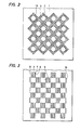
- Figure 2 is a front view of the printed circuit card of Figure 1 with the cooling plate removed;
- Figure 3 is a front view of the cooling plate of Figure 1;
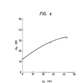
- Figure 4 is a diagram showing the characteristics of this invention;
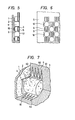
- Figure 5 is a simplified vertical cross section of another embodiment of this invention;
- Figure 6 is a front view of the cooling plate of Figure 5; and
- Figure 7 is a perspective view, partially cut away, of still another embodiment of this invention.
- The first embodiment of this invention will be explained referring to Figures 1 through 3.
- The printed
circuit card 1 hasmany semiconductor chips 2 mounted thereon. Astud 4 made of a cylindrical, heat conducting member is secured to the top of eachsemiconductor chip 2. Between the adjacent printedcircuit cards 1 are inserted aflat cooling plate 3 which has acooling water passage 5 in it. A large number ofthin fins 6, arranged parallel to each other with small gaps therebetween, are attached to thecooling plate 3. Thesefins 6 are arranged so that they enclose thestud 4. Thefins 6 all align parallel to the direction of gravity. The area where thechip stud 4 is inserted is aspace 9. A plurality ofprinted circuit cards 1 andcooling plates 3 are alternated with each other and submerged in a volatile liquid 11 (such as flon, perfluorocarbon compound, alcohol) in the enclosedcontainer 10. - A part of the
cooling plate 3 extends upward into avapor space 12 to form anauxiliary condensing surface 13.Water piping 14 is provided to introduce water into thecooling water passage 5 in thecooling plate 3. - It is desirable that a
resilient member 15 be inserted between the end of thefins 6 and the printedcircuit card 1 and that thesemiconductor chip 2 andstud 4 be completely enclosed by thefins 8. - The
stud 4 has a porous surface. - Next, the action of this embodiment is described in the following.
- The heat produced by the
semiconductor chip 2 is transmitted to thestud 4 and, through the porous surface of the stud, boils thevolatile liquid 11. - The vapor bubbles thus formed, being buoyant, rise upward and go into the
narrow gaps 7 between thefins 6. If the gap size is smaller than the bubble, the vapor directly contacts thefins 6. The cooling water flowing in thepassage 5 of thecooling plate 3 cools thecooling plate 3 andfins 6. Consequently the vapor condenses into liquid at the fin surface. The condensed liquid is drawn down by the force gravity and returns to the region around thestud 4. If there is aresilient member 15 provided between the end of thefins 6 and the printedcircuit card 1, and if eachsemiconductor chip 2 andstud 4 are enclosed completely byfins 6, then the vapor bubbles produced at thestud 4 all enter thenarrow gaps 7 between thefins 6, which enhance the condensing heat transfer coefficient. Where all thefins 6 are equal in length in the direction of gravity, the vapor bubbles enter and are distributed almost uniformly, among all the gaps between thefins 6, improving the condensing heat transfer coefficient. - A part of the vapor that has passed through the
fin gaps 7 collects in thevapor space 12 in the upper part of the enclosedcontainer 10 where it is condensed by theauxiliary condensing surface 13. - With this embodiment, since vapor condensation is performed for each semiconductor chip, all semiconductor chips can be cooled uniformly.
- Next, the representative dimensions of this embodiment are given below. The semiconductor chip is square with each side measuring 2 to 20 mm; the stud diameter is about the same as the side of the chip. The fins attached to the cooling plate are about 0.1 to 1.0 mm thick; the gap between fins is about 0.1 to 1.0 mm. The material of the fins is preferably chosen from those which have high thermal conductivity such as copper, aluminum, and silicon carbide.
- Figure 4 shows the result of experiment regarding the condensing heat conducting performance of this embodiment. In the experiment, the fin thickness is 0.3 mm; fin gaps are 0.2 mm each; fin length is 11 mm; fin height is 5.4 mm; the number of fins used is 25; and the liquid is perfluoro normal hexane.
- The temperature difference between the liquid and the cooling plate in this experiment is about 12°C. Let us look at the relation between the heat generated by a single semiconductor chip Qt and the heat removed by the fins Qd. It is seen that the plate removes about 30 W for each chip. The reason that the heat removed by the plate Qd is greater than Qt when the ;hip-generated heat Qt is below 30 W is that the liquid is supercooled while condensation is taking place. Further increase in the temperature difference between the liquid and the cooling plate will increase the heat removed by the fins.
- Figures 5 and 6 show another embodiment of this invention. In this embodiment, the
fins 6 are made small in height and where there is no fin a hole is formed in the cooling plate to insert the stud. - The
cooling plate 3 and thestud 4 are equal in height to make the cooling structure small. Instead offins 6, a large number of fine wires may be attached to thecooling plate 3. - In another embodiment shown in Figure 7, the
fins 6 attached to thecooling plate 3 are formed into rings (or a female screw). The heat of the chip is conveyed to thestud 4 which boils the nearbyliquid producing bubbles 40. Most of the bubbles are arrested between the ring-like fins 6 and trapped in theupper part 60 of the grooves of the fins. - The vapor trapped in the
upper part 60 of the fin grooves condenses on the groove wall and is drawn into thenarrow recess 61 of the groove by capillary attraction. The condensed liquid now moves down theperipheral surface 62 of thenarrow recess 61. In this way, almost all the vapor produced from each chip condenses near the chip. A small amount of vapor that has not been arrested by the cooling plate fins which enclose thestud 4 moves up and reaches the upper part of the container where it condenses into a thin layer of liquid hwich moves down returning to the liquid bath. - The recess of the cooling plate in which the stud is inserted has a large heat conducting area provided by the fins. Since the fins are used, provision of such a large heat conducting area does not result in any increase in the size of the cooling apparatus.
- Although in this embodiment explanation is given to only 'the case where the stud is secured to the back of the chip, it is also possible to make the stud axially movable and while in the state of being pressed by the spring.
Claims (4)
Applications Claiming Priority (2)
| Application Number | Priority Date | Filing Date | Title |
|---|---|---|---|
| JP243958/83 | 1983-12-26 | ||
| JP58243958A JPS60136352A (en) | 1983-12-26 | 1983-12-26 | Cooling device for integrated circuit chip |
Publications (2)
| Publication Number | Publication Date |
|---|---|
| EP0167665A1 true EP0167665A1 (en) | 1986-01-15 |
| EP0167665B1 EP0167665B1 (en) | 1988-06-29 |
Family
ID=17111565
Family Applications (1)
| Application Number | Title | Priority Date | Filing Date |
|---|---|---|---|
| EP84114163A Expired EP0167665B1 (en) | 1983-12-26 | 1984-11-23 | Apparatus for cooling integrated circuit chips |
Country Status (3)
| Country | Link |
|---|---|
| EP (1) | EP0167665B1 (en) |
| JP (1) | JPS60136352A (en) |
| DE (1) | DE3472501D1 (en) |
Cited By (4)
| Publication number | Priority date | Publication date | Assignee | Title |
|---|---|---|---|---|
| EP0200221A3 (en) * | 1985-04-30 | 1988-10-05 | Fujitsu Limited | Evaporation cooling module for semiconductor devices |
| GB2226708A (en) * | 1988-12-07 | 1990-07-04 | Sundstrand Corp | Cooling electronic circuit boards |
| WO2021231768A1 (en) * | 2020-05-13 | 2021-11-18 | Microsoft Technology Licensing, Llc | Systems and methods for vapor management in immersion cooling |
| WO2023135488A3 (en) * | 2022-01-15 | 2023-08-24 | Liquidstack Holding B.V. | Baffle assembly for use in an immersion cooling system |
Families Citing this family (2)
| Publication number | Priority date | Publication date | Assignee | Title |
|---|---|---|---|---|
| US5198889A (en) * | 1990-06-30 | 1993-03-30 | Kabushiki Kaisha Toshiba | Cooling apparatus |
| GB201919289D0 (en) | 2019-12-24 | 2020-02-05 | Iceotope Group Ltd | Cooling module |
Citations (1)
| Publication number | Priority date | Publication date | Assignee | Title |
|---|---|---|---|---|
| EP0007015A1 (en) * | 1978-07-11 | 1980-01-23 | International Business Machines Corporation | Device for cooling semiconductor chips with monolithic integrated circuits |
-
1983
- 1983-12-26 JP JP58243958A patent/JPS60136352A/en active Granted
-
1984
- 1984-11-23 EP EP84114163A patent/EP0167665B1/en not_active Expired
- 1984-11-23 DE DE8484114163T patent/DE3472501D1/en not_active Expired
Patent Citations (1)
| Publication number | Priority date | Publication date | Assignee | Title |
|---|---|---|---|---|
| EP0007015A1 (en) * | 1978-07-11 | 1980-01-23 | International Business Machines Corporation | Device for cooling semiconductor chips with monolithic integrated circuits |
Non-Patent Citations (1)
| Title |
|---|
| IBM TECHNICAL DISCLOSURE BULLETIN, vol. 10, no. 10, March 1968, pages 1559-1960, New York, US; R.C.CHU et al.: "Thermal card and deflector system for augmenting emersion cooling" * |
Cited By (5)
| Publication number | Priority date | Publication date | Assignee | Title |
|---|---|---|---|---|
| EP0200221A3 (en) * | 1985-04-30 | 1988-10-05 | Fujitsu Limited | Evaporation cooling module for semiconductor devices |
| GB2226708A (en) * | 1988-12-07 | 1990-07-04 | Sundstrand Corp | Cooling electronic circuit boards |
| WO2021231768A1 (en) * | 2020-05-13 | 2021-11-18 | Microsoft Technology Licensing, Llc | Systems and methods for vapor management in immersion cooling |
| US12484189B2 (en) | 2020-05-13 | 2025-11-25 | Microsoft Technology Licensing, Llc | Systems and methods for vapor management in immersion cooling |
| WO2023135488A3 (en) * | 2022-01-15 | 2023-08-24 | Liquidstack Holding B.V. | Baffle assembly for use in an immersion cooling system |
Also Published As
| Publication number | Publication date |
|---|---|
| DE3472501D1 (en) | 1988-08-04 |
| EP0167665B1 (en) | 1988-06-29 |
| JPS60136352A (en) | 1985-07-19 |
| JPH0423830B2 (en) | 1992-04-23 |
Similar Documents
| Publication | Publication Date | Title |
|---|---|---|
| US4694378A (en) | Apparatus for cooling integrated circuit chips | |
| US5097385A (en) | Super-position cooling | |
| EP0031448B1 (en) | Thermal conduction module for integrated circuit chips | |
| DE4121447C2 (en) | Air-cooled heat exchanger for multi-chip assemblies | |
| US4203129A (en) | Bubble generating tunnels for cooling semiconductor devices | |
| EP0169270B1 (en) | Cooling device of semiconductor chips | |
| US4704658A (en) | Evaporation cooling module for semiconductor devices | |
| US4573067A (en) | Method and means for improved heat removal in compact semiconductor integrated circuits | |
| US4450472A (en) | Method and means for improved heat removal in compact semiconductor integrated circuits and similar devices utilizing coolant chambers and microscopic channels | |
| US6263959B1 (en) | Plate type heat pipe and cooling structure using it | |
| US6037658A (en) | Electronic package with heat transfer means | |
| JPH088421B2 (en) | Heat dissipation device | |
| EP0033836B1 (en) | Heat transfer connection in a cooling module | |
| WO2002041395A2 (en) | A high-performance fin configuration for air-cooled heat dissipation device | |
| JPH05243441A (en) | Heat dissipation device | |
| US20090166003A1 (en) | Heat spreader with vapor chamber | |
| DE102018118070A1 (en) | Monolithic phase change heat dissipation device | |
| US11139226B2 (en) | Semiconductor package structure and assembly structure | |
| USRE35721E (en) | Cooling device of semiconductor chips | |
| EP0253126B1 (en) | Heat sink | |
| EP0167665B1 (en) | Apparatus for cooling integrated circuit chips | |
| JP2026042785A (en) | Evaporator assembly, vapor chamber, and method for manufacturing vapor chamber | |
| US4757370A (en) | Circuit package cooling technique with liquid film spreading downward across package surface without separation | |
| JP2506885B2 (en) | Semiconductor device | |
| JP2562180B2 (en) | Boiling cooling type semiconductor device |
Legal Events
| Date | Code | Title | Description |
|---|---|---|---|
| PUAI | Public reference made under article 153(3) epc to a published international application that has entered the european phase |
Free format text: ORIGINAL CODE: 0009012 |
|
| 17P | Request for examination filed |
Effective date: 19841123 |
|
| AK | Designated contracting states |
Designated state(s): DE GB |
|
| 17Q | First examination report despatched |
Effective date: 19871013 |
|
| GRAA | (expected) grant |
Free format text: ORIGINAL CODE: 0009210 |
|
| AK | Designated contracting states |
Kind code of ref document: B1 Designated state(s): DE GB |
|
| REF | Corresponds to: |
Ref document number: 3472501 Country of ref document: DE Date of ref document: 19880804 |
|
| PLBE | No opposition filed within time limit |
Free format text: ORIGINAL CODE: 0009261 |
|
| STAA | Information on the status of an ep patent application or granted ep patent |
Free format text: STATUS: NO OPPOSITION FILED WITHIN TIME LIMIT |
|
| 26N | No opposition filed | ||
| REG | Reference to a national code |
Ref country code: GB Ref legal event code: IF02 |
|
| PGFP | Annual fee paid to national office [announced via postgrant information from national office to epo] |
Ref country code: GB Payment date: 20021028 Year of fee payment: 19 |
|
| PGFP | Annual fee paid to national office [announced via postgrant information from national office to epo] |
Ref country code: DE Payment date: 20021205 Year of fee payment: 19 |
|
| PG25 | Lapsed in a contracting state [announced via postgrant information from national office to epo] |
Ref country code: GB Free format text: LAPSE BECAUSE OF NON-PAYMENT OF DUE FEES Effective date: 20031123 |
|
| PG25 | Lapsed in a contracting state [announced via postgrant information from national office to epo] |
Ref country code: DE Free format text: LAPSE BECAUSE OF NON-PAYMENT OF DUE FEES Effective date: 20040602 |
|
| GBPC | Gb: european patent ceased through non-payment of renewal fee |
Effective date: 20031123 |