EP0167431A1 - Drive circuit for switching with electrical isolation and infinitely variable conduction time - Google Patents
Drive circuit for switching with electrical isolation and infinitely variable conduction time Download PDFInfo
- Publication number
- EP0167431A1 EP0167431A1 EP85401094A EP85401094A EP0167431A1 EP 0167431 A1 EP0167431 A1 EP 0167431A1 EP 85401094 A EP85401094 A EP 85401094A EP 85401094 A EP85401094 A EP 85401094A EP 0167431 A1 EP0167431 A1 EP 0167431A1
- Authority
- EP
- European Patent Office
- Prior art keywords
- transistor
- circuit
- rectifier bridge
- output
- current
- Prior art date
- Legal status (The legal status is an assumption and is not a legal conclusion. Google has not performed a legal analysis and makes no representation as to the accuracy of the status listed.)
- Granted
Links
Images
Classifications
-
- H—ELECTRICITY
- H02—GENERATION; CONVERSION OR DISTRIBUTION OF ELECTRIC POWER
- H02M—APPARATUS FOR CONVERSION BETWEEN AC AND AC, BETWEEN AC AND DC, OR BETWEEN DC AND DC, AND FOR USE WITH MAINS OR SIMILAR POWER SUPPLY SYSTEMS; CONVERSION OF DC OR AC INPUT POWER INTO SURGE OUTPUT POWER; CONTROL OR REGULATION THEREOF
- H02M3/00—Conversion of dc power input into dc power output
- H02M3/02—Conversion of dc power input into dc power output without intermediate conversion into ac
- H02M3/04—Conversion of dc power input into dc power output without intermediate conversion into ac by static converters
- H02M3/10—Conversion of dc power input into dc power output without intermediate conversion into ac by static converters using discharge tubes with control electrode or semiconductor devices with control electrode
- H02M3/145—Conversion of dc power input into dc power output without intermediate conversion into ac by static converters using discharge tubes with control electrode or semiconductor devices with control electrode using devices of a triode or transistor type requiring continuous application of a control signal
- H02M3/155—Conversion of dc power input into dc power output without intermediate conversion into ac by static converters using discharge tubes with control electrode or semiconductor devices with control electrode using devices of a triode or transistor type requiring continuous application of a control signal using semiconductor devices only
-
- H—ELECTRICITY
- H02—GENERATION; CONVERSION OR DISTRIBUTION OF ELECTRIC POWER
- H02M—APPARATUS FOR CONVERSION BETWEEN AC AND AC, BETWEEN AC AND DC, OR BETWEEN DC AND DC, AND FOR USE WITH MAINS OR SIMILAR POWER SUPPLY SYSTEMS; CONVERSION OF DC OR AC INPUT POWER INTO SURGE OUTPUT POWER; CONTROL OR REGULATION THEREOF
- H02M1/00—Details of apparatus for conversion
- H02M1/08—Circuits specially adapted for the generation of control voltages for semiconductor devices incorporated in static converters
-
- H—ELECTRICITY
- H03—ELECTRONIC CIRCUITRY
- H03K—PULSE TECHNIQUE
- H03K17/00—Electronic switching or gating, i.e. not by contact-making and –breaking
- H03K17/51—Electronic switching or gating, i.e. not by contact-making and –breaking characterised by the components used
- H03K17/56—Electronic switching or gating, i.e. not by contact-making and –breaking characterised by the components used by the use, as active elements, of semiconductor devices
- H03K17/60—Electronic switching or gating, i.e. not by contact-making and –breaking characterised by the components used by the use, as active elements, of semiconductor devices the devices being bipolar transistors
- H03K17/601—Electronic switching or gating, i.e. not by contact-making and –breaking characterised by the components used by the use, as active elements, of semiconductor devices the devices being bipolar transistors using transformer coupling
Definitions
- the present invention relates to the control circuits of semiconductor components operating in switching mode, for example power transistors, Darlington assemblies, thyristors, thyristors lockable by the trigger. These switching elements are used for energy conversion, for example for producing power supplies for welding stations, variable speed drives, emergency power supplies, etc.
- controlled component is a power transistor (control by the base) but the invention is also applicable to other components such as those which are indicated above.
- Energy converters operate on the very general principle of switching a power component with a variable frequency and / or conduction duty cycle in large proportions.
- the switching of the component is ensured by a control circuit which receives a control signal having this frequency and this duty cycle, and which moreover receives a supply energy necessary for its operation.
- Galvanic isolation is necessary for example when the energy converter is a bridge converter in which at least one component must have its emitter has floating potential and not to a fixed ground potential, which makes it more difficult to control. Isolation is also desirable for safety reasons or to prevent a failure of a power component from destroying the circuits for developing the control signal.
- Another constraint to which we wish to respond is also the possibility not only of applying a negative base (or trigger) control current for blocking the component, but also of maintaining a negative bias on this base throughout the duration of blocking.
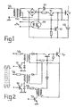
- Figure 1 shows an example of a control circuit of a power transistor Tp.
- the power supply of this circuit is done through a galvanic isolation transformer TR1 receiving an alternating current at 50 Hz or at higher frequency (20 kilohertz for example).
- the secondary of the transformer TR is a winding having a midpoint connected to the emitter of the transistor Tp.
- the voltage across the rectifier is rectified by a diode bridge and filtered by two capacitors C1 and C2.
- the actual control circuit consists of two transistors TI and T2, the emitters of which are connected to the base of the power transistor Tp.
- the transistors Tl and T2 are controlled by the output of an optoelectronic coupler CO receiving an all-or-nothing control signal and ensuring the transmission of this signal with galvanic isolation.
- the transistor TI is made conductive by this signal, the transistor T2 is blocked and the base of the transistor Tp receives a positive current which makes this transistor conductive.
- T2 When T1 is blocked, T2 is made conductive and a negative current is extracted from the base of the transistor Tp which is therefore blocked.
- the optoelectronic coupler is replaced by a small transformer driven in short positive and negative pulses and followed by a flip-flop; the speed of transmission of the control signal is greater but the sensitivity to parasites is also greater and its effect is even more annoying because of the flip-flop which can maintain an incorrect state for a long time (memorization of the imposed state by a parasite).
- FIG. 2 Another type of control circuit is shown in FIG. 2. It has the advantage of being very insensitive to interference but it has the drawback of requiring three transformers for each transistor to be switched; on the other hand, it does not make it possible to maintain a negative bias on the base of the transistor Tp when the latter is blocked.
- This diagram works as follows: three transistors TI, T2, T3 each control a primary transformer winding. TI and T2 are switched on alternately (at a high frequency) while T3 is blocked; the transistor Tp then receives a positive base current alternately from the transformers controlled by TI and T2 respectively. Tp is therefore conductive.
- T3 To block Tp, we make T3 conductive for a short time, at the same time as we block TI and T2. A temporary negative base current is then extracted from the base of Tp which is blocked.
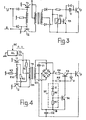
- FIG. 3 Another known control circuit diagram is shown in FIG. 3. This diagram uses only one transformer used to transmit both the energy required for the control circuit and the conduction and blocking control signal from the power transistor Tp.
- the transformer TR has a primary winding and two secondary windings, one of which is coupled to the primary with two transistors TI and T2 to constitute an oscillator, and the other of which is galvanically isolated from the primary to supply the basic control circuit properly said.
- the oscillator can be started or blocked from two inputs acting on the bases of the TI and T2 transistors.
- an oscillating signal is received or not received depending on whether or not the oscillator oscillates on the primary side.
- the secondary oscillating signal when it exists, establishes a positive base current making the transistor Tp conductive.
- a threshold detector DS detects this disappearance and momentarily conducts a transistor T3 which extracts a negative current from the base of the transistor Tp, with the help of a capacitor C which had charged during the conduction of the transistor Tp.
- the present invention provides a control circuit which makes it possible to best resolve all of the problems encountered in known circuits.
- the control circuit intended to ensure the switching of a power semiconductor component as a function of the binary state of a switching control signal, with galvanic isolation between this control signal and the component, comprises a transformer having a primary winding and at least one secondary winding, an oscillator supplied by a DC voltage and providing an oscillating signal to the primary winding, a rectifier bridge at the output of the secondary winding, and a transistor circuit supplied by the rectifier bridge and providing to a power component control electrode either a conduction current of the power component, or a blocking current, depending on the control signal.
- the secondary winding is in principle a mid-point winding, this point defining a reference potential and the rectifier bridge providing positive and negative voltages for the supply of the transistor circuit.
- the semiconductor component whose switching is to be ensured is a power transistor Tp, of the NPN type.
- the circuit controlled by this transistor is not shown. Only the transistor control circuit is shown.
- the control is carried out by a binary control signal SC having two possible states, one establishing the conduction of the transistor Tp, the other establishing its blocking.
- the primary winding EPI there is a primary winding EPI, a main secondary winding ES and an auxiliary secondary winding ES2.
- the primary winding EP1 and the auxiliary secondary winding ES2 are located galvanically on the side of the control signal SC.
- the main secondary winding ES1 is located galvanically on the side of the power transistor and the intermediate tap of this winding is moreover connected directly to the emitter of the power transistor; the potential of this emitter defines a reference with respect to which it will be seen that the base of the transistor Tp can be positively or negatively biased.
- the primary winding EP of the transformer receives alternating electrical energy from an oscillating circuit constituted in a conventional manner (which is essentially found in Figure 3) from two transistors T1 and T2, from the primary winding EP 1 itself and the auxiliary secondary winding ES2.
- This oscillating circuit is constituted in the following way: the transistors have their emitter connected to a ground (ground on the side of the control signal), have their collector respectively connected to one end of the primary winding, and have their base connected respec - tivment each at one end of the auxiliary winding; a resistor R 1 connects the collector of transistor Tl to the base of transistor T2; a resistor R2 connects the collector of transistor T2 at the base of transistor Tl; a resistor R3 connects the intermediate (middle) tap of the winding ES2 to the ground. Finally, a direct supply voltage is applied to the intermediate (middle) tap of the primary winding EP 1.
- the diagram of Figure 4 differs from that of Figure 3 (for the part which is located galvanically on the side of the control signal) on two aspects: the first is the fact that there is not in Figure 4 control terminals connected to the bases of the transistors to establish or stop the oscillation of the oscillator; the oscillator always oscillates; ie the second is the fact that the supply voltage in FIG. 4 does not come from a fixed bias source but comes from a supply AL controlled by the control signal SC and capable of supplying, according to the state of this signal, two supply voltages of different non-zero values Va and Vb (of the same sign obviously, corresponding to the type of tansistors T and T2: positive sign for NPN transistors).
- the voltages Va and Vb are both sufficient to ensure on the one hand a stable oscillation of the oscillator (at a frequency of a few tens of kilohertz so that the transformer TR remains small) and on the other hand a transmission of sufficient energy through the main secondary winding ES1, so that the circuit supplied by this secondary operates normally and allows adequate positive or negative polarization of the base of the transistor Tp both when the supply voltage is set to Va and when 'it has the value Vb.
- rectifier bridge RD On the side which is galvanically connected to the transistor Tp, there is a rectifier bridge RD with four diodes arranged at the terminals of the main secondary winding ES1, and filtering capacitors of small value, respectively CI and C2, between each output of the rectifier bridge RD and the center tap of the secondary winding.
- the rectifier bridge Compared to the reference potential defined by this center tap and applied to the emitter of the power transistor, the rectifier bridge therefore supplies rectified and filtered supply voltages, positive and negative (in principle symmetrical).
- the positive output terminal is designated by the letter A, the negative terminal by the letter B.
- a voltage level detector DT is placed between terminals A and B to indicate whether the rectified voltage supplied by the bridge corresponds to a primary supply by the voltage Va or on the contrary to a primary supply by the voltage Vb.
- This voltage level detector controls a circuit with two transistors T3 and T4, connected to the base of the transistor Tp, to cause this circuit to establish a positive base current, ensuring the conduction and the conduction maintenance of the transistor Tp, when the detected voltage corresponds to a supply Va, and to establish on the contrary a negative base current, ensuring not only an extraction of base current necessary for blocking the transistor Tp, but also the maintenance of a negative base bias originating of terminal B, when the detected voltage corresponds to a supply Vb.
- the transistor circuit thus controlled is very simple: it comprises a transistor T3 having its emitter connected to the base of the power transistor, its collector connected through a limiting resistor R4 to the positive output terminal A of the rectifier bridge, and its base connected by a bias resistor R5 to this terminal A.
- a diode D is mounted in antiparallel across the terminals of the base-emitter junction of the transistor T3, that is to say that for an NPN transistor the anode of the diode is connected to the emitter and its cathode to the base.
- a transistor T4 has its base connected to the output of the detector level DT, its emitter connected to terminal B and its collector connected to the base of transistor T3.
- the voltage level detector can also be very simple: it comprises in FIG. 4 a zener diode Z in series with a bridge of current limiting resistors R6, R7, the whole connected between the terminals A and B, the output of the detector being taken at the junction point of resistors R6 and R7.
- the zener diode When the primary is supplied with the voltage Va, the zener diode remains blocked, the supply voltage between the terminals A and B being lower than the nominal voltage of this diode.
- the transistor T4 remains blocked because its base receives no current; the transistor T3 is on the contrary normally polarized and supplies from terminal A a positive basic current maintaining the transistor Tp conductive.
- the zener diode When the primary power is supplied with the voltage Vb, the zener diode is conducting because the voltage between the terminals A and B is now greater than its nominal voltage; transistor T4 becomes highly conductive, its collector goes to the potential of terminal B (negative), which has the effect of firstly lowering the potential of the base of transistor T3 below the potential of its emitter and therefore to block it, and on the other hand to extract a negative current from the base of the transistor Tp through the diode D, extraction which is necessary to ensure rapid blocking of the transistor Tp.
- the conductive transistor T4 maintains a negative bias of the base of the transistor Tp until the control signal SC changes state and reduces the primary supply voltage to Va.
- the circuit which has just been described is entirely applicable to the control of other semiconductor elements and more particularly to the control of thyristors lockable by the trigger.
Abstract
Description
La présente invention concerne les circùits de commande de composants semiconducteurs fonctionnant en commutation, par exemple des transistors de puissance, des montages Darlington, des thyristors, des thyristors blocables par la gâchette. Ces éléments de commutation sont utilisés pour la conversion d'énergie, par exemple pour réaliser des alimentations de postes de soudure, des variateurs de vitesse, des alimentations de secours etc...The present invention relates to the control circuits of semiconductor components operating in switching mode, for example power transistors, Darlington assemblies, thyristors, thyristors lockable by the trigger. These switching elements are used for energy conversion, for example for producing power supplies for welding stations, variable speed drives, emergency power supplies, etc.
Dans tout ce qui suit, on considère à titre d'exemple que le composant commandé est un transistor de puissance (commande par la base) mais l'invention est applicable aussi à d'autres composants tels que ceux qui sont indiqués ci-dessus.In all that follows, it is considered by way of example that the controlled component is a power transistor (control by the base) but the invention is also applicable to other components such as those which are indicated above.
Les convertisseurs d'énergie fonctionnent sur le principe très général d'une commutation d'un composant de puissance avec une fréquence et/ou un rapport cyclique de conduction variable dans de larges proportions. La commutation du composant est assurée par un circuit de commande qui reçoit un signal de commande ayant cette fréquence et ce rapport cyclique, et qui reçoit par ailleurs une énergie d'alimentation nécessaire à son fonctionnement.Energy converters operate on the very general principle of switching a power component with a variable frequency and / or conduction duty cycle in large proportions. The switching of the component is ensured by a control circuit which receives a control signal having this frequency and this duty cycle, and which moreover receives a supply energy necessary for its operation.
Dans certaines applications on peut souhaiter répondre a deux contraintes particulières qui sont:
- - d'une part, un isolement galvanique entre le circuit de commande de l'élément de commutation et le circuit d'élaboration du signal de commande proprement dit :
- - d'autre part une possibilité de variation très large, si possible de zéro a l'infini, des durées de conduction et des durées de blocage du composant de commutation.
- on the one hand, a galvanic isolation between the control circuit of the switching element and the circuit for producing the control signal proper:
- - on the other hand, a very wide variation possibility, if possible from zero to infinity, of the conduction durations and of the blocking durations of the switching component.
L'isolement galvanique est nécessaire par exemple lorsque le convertisseur d'énergie est un convertisseur en pont dans lequel au moins un composant doit avoir son émetteur a un potentiel flottant et non à un potentiel fixe de masse, ce qui rend sa commande plus difficile. L'isolement est aussi souhaitable pour des raisons de sécurité ou pour éviter qu'une panne d'un composant de puissance n'entraîne la destruction des circuits d'élaboration du signal de commande.Galvanic isolation is necessary for example when the energy converter is a bridge converter in which at least one component must have its emitter has floating potential and not to a fixed ground potential, which makes it more difficult to control. Isolation is also desirable for safety reasons or to prevent a failure of a power component from destroying the circuits for developing the control signal.
La variation très large du rapport cyclique ou de la fréquence, donc plus généralement des durées de conduction et de blocage, est utile par exemple pour des onduleurs à très basse fréquence.The very wide variation of the duty cycle or of the frequency, therefore more generally of the conduction and blocking times, is useful for example for very low frequency inverters.
Une autre contrainte à laquelle on désire répondre est aussi la possibilité non seulement d'appliquer un courant de commande de base (ou de gâchette) négatif pour le blocage du composant, mais encore de maintenir une polarisation négative sur cette base pendant toute la durée de blocage.Another constraint to which we wish to respond is also the possibility not only of applying a negative base (or trigger) control current for blocking the component, but also of maintaining a negative bias on this base throughout the duration of blocking.
Les circuits de commande de commutation proposés jusqu'à maintenant ne répondent que partiellement à ces divers impératifs et présentent des inconvénients importants, notamment du point de vue du coût de réalisation et de la fiabilité de fonctionnement.The switching control circuits proposed so far only partially meet these various requirements and have significant drawbacks, in particular from the point of view of the cost of production and reliability of operation.
Ainsi, la figure 1 représente un exemple de circuit de commande d'un transistor de puissance Tp.Thus, Figure 1 shows an example of a control circuit of a power transistor Tp.
L'alimentation en énergie de ce circuit se fait à travers un transformateur d'isolement galvanique TR1 recevant un courant alternatif à 50 Hz ou à plus haute fréquence (20 kilohertz par exemple).The power supply of this circuit is done through a galvanic isolation transformer TR1 receiving an alternating current at 50 Hz or at higher frequency (20 kilohertz for example).
Le secondaire du transformateur TR est un enroulement ayant un point milieu relié à l'émetteur du transistor Tp.The secondary of the transformer TR is a winding having a midpoint connected to the emitter of the transistor Tp.
La tension aux bornes du redresseur est redressée par un pont de diodes et filtrée par deux capacités C1 et C2. Le circuit de commande proprement dit est constitué par deux transistors TI et T2 dont les émetteurs sont reliés à la base du transistor de puissance Tp. Les transistors Tl et T2 sont commandés par la sortie d'un coupleur optoélectronique CO recevant un signal de commande en tout ou rien et assurant la transmission de ce signal avec isolement galvanique. Lorsque le transistor TI est rendu conducteur par ce signal, le transistor T2 est bloqué et la base du transistor Tp reçoit un courant positif qui rend conducteur ce transistor.The voltage across the rectifier is rectified by a diode bridge and filtered by two capacitors C1 and C2. The actual control circuit consists of two transistors TI and T2, the emitters of which are connected to the base of the power transistor Tp. The transistors Tl and T2 are controlled by the output of an optoelectronic coupler CO receiving an all-or-nothing control signal and ensuring the transmission of this signal with galvanic isolation. When the transistor TI is made conductive by this signal, the transistor T2 is blocked and the base of the transistor Tp receives a positive current which makes this transistor conductive.
Lorsque T1 est bloqué, T2 est rendu conducteur et un courant négatif est extrait de la base du transistor Tp qui est donc bloqué.When T1 is blocked, T2 is made conductive and a negative current is extracted from the base of the transistor Tp which is therefore blocked.
L'inconvénient de ce type de circuit est'd'une part la lenteur de la transmission optique du signal de commande par le coupleur, d'autre part la sensibilité aux parasites susceptibles de déclencher intempestivement l'élément de commutation, et enfin la nécessité d'utiliser plusieurs coupleurs opto-électroniques dans le cas d'un convertisseur en pont.The drawback of this type of circuit is firstly the slowness of the optical transmission of the control signal by the coupler, secondly the sensitivity to parasites liable to inadvertently trigger the switching element, and finally the need to use several opto-electronic couplers in the case of a bridge converter.
Dans certains cas, le coupleur optoélectronique est remplacé par un petit transformateur attaqué en impulsions courtes positives et négatives et suivi d'une bascule bistable ; la rapidité de transmission du signal de commande est plus grande mais la sensibilité aux parasites est également plus gande et son effet est encore plus gênant à cause de la bascule bistable qui peut maintenir un état incorrect pendant une durée iongue (mémorisation de l'état imposé par un parasite).In some cases, the optoelectronic coupler is replaced by a small transformer driven in short positive and negative pulses and followed by a flip-flop; the speed of transmission of the control signal is greater but the sensitivity to parasites is also greater and its effect is even more annoying because of the flip-flop which can maintain an incorrect state for a long time (memorization of the imposed state by a parasite).
Un autre type de circuit de commande est représenté à la figure 2. Il a l'avantage d'être peu sensible aux parasites mais il a l'inconvénient de nécessiter trois transformateurs pour chaque transistor à commuter ; d'autre part il ne permet pas de maintenir une polarisation négative sur la base du transistor Tp lorsque celui- ci est bloqué. Ce schéma fonctionne de la manière suivante : trois transistors TI, T2, T3 commandent chacun un enroulement primaire de transformateur. TI et T2 sont rendus conducteurs de manière alternée (à une fréquence élevée) pendant que T3 est bloqué ; le transistor Tp reçoit alors un courant de base positif issu alternativement des transformateurs commandés par TI et T2 respectivement. Tp est donc conducteur.Another type of control circuit is shown in FIG. 2. It has the advantage of being very insensitive to interference but it has the drawback of requiring three transformers for each transistor to be switched; on the other hand, it does not make it possible to maintain a negative bias on the base of the transistor Tp when the latter is blocked. This diagram works as follows: three transistors TI, T2, T3 each control a primary transformer winding. TI and T2 are switched on alternately (at a high frequency) while T3 is blocked; the transistor Tp then receives a positive base current alternately from the transformers controlled by TI and T2 respectively. Tp is therefore conductive.
Pour bloquer Tp, on rend T3 conducteur pendant une courte durée, en même temps qu'on bloque TI et T2. Un courant de base négatif temporaire est alors extrait de la base de Tp qui se bloque.To block Tp, we make T3 conductive for a short time, at the same time as we block TI and T2. A temporary negative base current is then extracted from the base of Tp which is blocked.
Un autre schéma de circuit de commande connu est représenté à la figure 3. Ce schéma n'utilise qu'un seul transformateur servant à transmettre à la fois l'énergie nécessaire au circuit de commande et le signal de commande de conduction et de blocage du transistor de puissance Tp.Another known control circuit diagram is shown in FIG. 3. This diagram uses only one transformer used to transmit both the energy required for the control circuit and the conduction and blocking control signal from the power transistor Tp.
Le transformateur TR possède un enroulement primaire et deux enroulements secondaires, dont l'un est couplé au primaire avec deux transistors TI et T2 pour constituer un oscillateur, et dont l'autre est isolé galvaniquement du primaire pour alimenter le circuit de commande de base proprement dit.The transformer TR has a primary winding and two secondary windings, one of which is coupled to the primary with two transistors TI and T2 to constitute an oscillator, and the other of which is galvanically isolated from the primary to supply the basic control circuit properly said.
L'oscillateur peut être mis en route ou bloqué à partir de deux entrées agissant sur les bases des transistors TI et T2. Du côté du secondaire, un signal oscillant est reçu ou n'est pas reçu selon que l'oscillateur oscille ou non du côté du primaire. Le signal oscillant du secondaire, lorsqu'il existe, établit un courant de base positif rendant le transistor Tp conducteur. Lorsqu'il disparaît, un détecteur de seuil DS détecte cette disparition et rend momentanément conducteur un transistor T3 qui extrait un courant négatif de la base du transistor Tp, avec l'aide d'une capacité C qui s'était chargée pendant la conduction du transistor Tp.The oscillator can be started or blocked from two inputs acting on the bases of the TI and T2 transistors. On the secondary side, an oscillating signal is received or not received depending on whether or not the oscillator oscillates on the primary side. The secondary oscillating signal, when it exists, establishes a positive base current making the transistor Tp conductive. When it disappears, a threshold detector DS detects this disappearance and momentarily conducts a transistor T3 which extracts a negative current from the base of the transistor Tp, with the help of a capacitor C which had charged during the conduction of the transistor Tp.
Ce schéma a l'avantage de n'utiliser qu'un seul transformateur (petit car il fonctionne à haute fréquence : quelques dizaines de kilohertz) mais :
- - d'une part il n'y a pas de possibilité de maintien d'une polarisation négative de la base de Tp pendant les périodes de blocage, puisque l'oscillateur n'oscille plus et ne fournit donc plus d'énergie au circuit de commande,
- - et d'autre part la durée de conduction de Tp doit avoir une valeur minimale pour que la capacité C ait le temps de se charger suffisamment pour établir ensuite un courant négatif de blocage.
- - on the one hand there is no possibility of maintaining a negative polarization of the base of Tp during the blocking periods, since the oscillator no longer oscillates and therefore no longer supplies energy to the circuit ordered,
- - and on the other hand, the conduction time of Tp must have a minimum value so that the capacitance C has time to charge sufficiently to then establish a negative blocking current.
La présente invention propose un circuit de commande qui permet de résoudre au mieux l'ensemble des problèmes rencontrés dans les circuits connus.The present invention provides a control circuit which makes it possible to best resolve all of the problems encountered in known circuits.
Le circuit de commande, destiné à assurer la commutation d'un composant semiconducteur de puissance en fonction de l'état binaire d'un signal de commande de commutation, avec isolement galvanique entre ce signal de commande et le composant, comporte un transformateur ayant un enroulement primaire et au moins un enroulement secondaire, un oscillateur alimenté par une tension continue et fournissant un signal oscillant à l'enroulement primaire, un pont redresseur en sortie de l'enroulement secondaire, et un circuit à transistors alimenté par le pont redresseur et fournissant à une électrode de commande du composant de puissance soit un courant de mise en conduction du composant de puissance, soit un courant de blocage, selon le signal de commande.The control circuit, intended to ensure the switching of a power semiconductor component as a function of the binary state of a switching control signal, with galvanic isolation between this control signal and the component, comprises a transformer having a primary winding and at least one secondary winding, an oscillator supplied by a DC voltage and providing an oscillating signal to the primary winding, a rectifier bridge at the output of the secondary winding, and a transistor circuit supplied by the rectifier bridge and providing to a power component control electrode either a conduction current of the power component, or a blocking current, depending on the control signal.
Selon l'invention :
- a) il est prévu un moyen pour appliquer à l'oscillateur une tension d'alimentation continue pouvant prendre deux valeurs différentes non nulles en fonction du signal de commande, les deux valeurs étant suffisantes pour assurer l'oscillation de l'oscillateur et l'alimentation normale par le pont redresseur du circuit à transistors relié à l'électrode de commande du composant de puissance,
- b) un détecteur de niveau de tension est relié à la sortie du pont redresseur et commande le circuit à transistors pour établir soit un courant de mise en conduction, soit un courant de blocage, selon que le niveau de tension en sortie du pont redresseur correspond à une alimentation de l'oscillateur par la première valeur ou par la deuxième valeur de tension d'alimentation au primaire.
- a) a means is provided for applying a continuous supply voltage to the oscillator which can take two different non-zero values as a function of the control signal, the two values being sufficient to ensure the oscillation of the oscillator and the normal supply by the rectifier bridge of the transistor circuit connected to the power component control electrode,
- b) a voltage level detector is connected to the output of the rectifier bridge and controls the transistor circuit to establish either a conduction current or a blocking current, depending on whether the voltage level at the output of the rectifier bridge corresponds to a supply of the oscillator by the first value or by the second value of primary supply voltage.
L'enroulement secondaire est en principe un enroulement à point-milieu, ce point définissant un potentiel de référence et le pont redresseur fournissant des tensions positive et négative pour l'alimentation du circuit à transistors.The secondary winding is in principle a mid-point winding, this point defining a reference potential and the rectifier bridge providing positive and negative voltages for the supply of the transistor circuit.
Le circuit préférentiel selon l'invention va maintenant être décrit plus en détail en référence aux dessins annexés dans lesquels :
- - les figures à 3 déjà décrites représentent divers exemples de circuits de commande connus,
- - la figure 4 représente le circuit selon l'invention.
- the figures to 3 already described represent various examples of known control circuits,
- - Figure 4 shows the circuit according to the invention.
Sur la figure 4, le composant semiconducteur dont la commutation est à assurer est un transistor de puissance Tp, de type NPN. Le circuit commandé par ce transistor n'est pas représenté. Seul le circuit de commande du transistor est représenté.In FIG. 4, the semiconductor component whose switching is to be ensured is a power transistor Tp, of the NPN type. The circuit controlled by this transistor is not shown. Only the transistor control circuit is shown.
La commande s'effectue par un signal de commande binaire SC ayant deux états possibles, l'un établissant la mise en conduction du transistor Tp, l'autre établissant son blocage.The control is carried out by a binary control signal SC having two possible states, one establishing the conduction of the transistor Tp, the other establishing its blocking.
Il y a un isolement galvanique complet entre le signal de commande SC et le transistor Tp et cet isolement est assuré par un transformateur TR ayant ici trois enroulements pourvus chacun d'une prise intermédiaire en principe médiane.There is complete galvanic isolation between the control signal SC and the transistor Tp and this isolation is ensured by a transformer TR having here three windings each provided with an intermediate tap in principle median.
Parmi les enroulements, on trouve un enroulement primaire EPI, un enroulement secondaire principal ES et un enroulement secondaire auxiliaire ES2. L'enroulement primaire EP1 et l'enroulement secondaire auxiliaire ES2 sont situés galvaniquement du côté du signal de commande SC. L'enroulement secondaire principal ES1 est situé galvaniquement du côté du transistor de puissance et la prise intermédiaire de cet enroulement est d'ailleurs reliée directement à l'émetteur du transistor de puissance ; le potentiel de cet émetteur définit une référence par rapport à laquelle on verra que la base du transistor Tp peut être polarisée positivement ou négativement.Among the windings, there is a primary winding EPI, a main secondary winding ES and an auxiliary secondary winding ES2. The primary winding EP1 and the auxiliary secondary winding ES2 are located galvanically on the side of the control signal SC. The main secondary winding ES1 is located galvanically on the side of the power transistor and the intermediate tap of this winding is moreover connected directly to the emitter of the power transistor; the potential of this emitter defines a reference with respect to which it will be seen that the base of the transistor Tp can be positively or negatively biased.
L'enroulement primaire EP du transformateur reçoit une énergie électrique alternative d'un circuit oscillant constitué d'une manière classique (que l'on retrouve pour l'essentiel sur la figure 3) a partir de deux transistors T1 et T2, de l'enroulement primaire EP 1 lui-même et de l'enroulement secondaire auxiliaire ES2. Ce circuit oscillant est constitué de la manière suivante : les transistors ont leur émetteur relié à une masse (masse du côté du signal de commande), ont leur collecteur relié respectivement chacun à une extrémité de l'enroulement primaire, et ont leur base reliée respec- tivment chacune à une extrémité de l'enroulement auxiliaire ; une résistance R1 relie le collecteur du transistor Tl à la base du transistor T2 ; une résistance R2 relie le collecteur du transistor T2 à la base du transistor Tl ; une résistance R3 relie la prise intermédiaire (médiane) de l'enroulement ES2 à la masse. Enfin, une tension continue d'alimentation est appliquée a la prise intermédiaire (médiane) de l'enroulement primaire EP 1.The primary winding EP of the transformer receives alternating electrical energy from an oscillating circuit constituted in a conventional manner (which is essentially found in Figure 3) from two transistors T1 and T2, from the primary winding EP 1 itself and the auxiliary secondary winding ES2. This oscillating circuit is constituted in the following way: the transistors have their emitter connected to a ground (ground on the side of the control signal), have their collector respectively connected to one end of the primary winding, and have their base connected respec - tivment each at one end of the auxiliary winding; a resistor R 1 connects the collector of transistor Tl to the base of transistor T2; a resistor R2 connects the collector of transistor T2 at the base of transistor Tl; a resistor R3 connects the intermediate (middle) tap of the winding ES2 to the ground. Finally, a direct supply voltage is applied to the intermediate (middle) tap of the primary winding EP 1.
Le schéma de la figure 4 se distingue de celui de la figure 3 (pour la partie qui est située galvaniquement du côté du signal de commande) sur deux aspects : le premier est le fait qu'il n'y a pas sur la figure 4 de bornes de commande reliées aux bases des transistors pour établir ou arrêter l'oscillation de l'oscillateur ; l'oscillateur oscille toujours ; ie deuxième est le fait que la tension d'alimentation sur la figure 4 n'est pas issue d'une source de polarisation fixe mais est issue d'une alimentation AL contrôlée par le signal de commande SC et susceptible de fournir, selon l'état de ce signal, deux tensions d'alimentation de valeurs différentes non nulles Va et Vb (de même signe évidemment, correspondant au type des tansistors T et T2 : signe positif pour des transistors NPN).The diagram of Figure 4 differs from that of Figure 3 (for the part which is located galvanically on the side of the control signal) on two aspects: the first is the fact that there is not in Figure 4 control terminals connected to the bases of the transistors to establish or stop the oscillation of the oscillator; the oscillator always oscillates; ie the second is the fact that the supply voltage in FIG. 4 does not come from a fixed bias source but comes from a supply AL controlled by the control signal SC and capable of supplying, according to the state of this signal, two supply voltages of different non-zero values Va and Vb (of the same sign obviously, corresponding to the type of tansistors T and T2: positive sign for NPN transistors).
En l'occurence, lorsque le signal de commande SC a un état correspondant à la conduction du transistor de puissance Tp, la tension fournie par l'alimentation est Va ; lorsque le signal SC a un état correspondant au blocage, la tension fournie est Vb supérieur a Va.In this case, when the control signal SC has a state corresponding to the conduction of the power transistor Tp, the voltage supplied by the power supply is Va; when the signal SC has a state corresponding to blocking, the voltage supplied is Vb greater than Va.
Les tensions Va et Vb sont toutes deux suffisantes pour assurer d'une part une oscillation stable de l'oscillateur (à une fréquence de quelques dizaines de kilohertz pour que le transformateur TR reste de petites dimensions) et d'autre part une transmission d'énergie suffisante à travers l'enroulement secondaire principal ES1, de sorte que le circuit alimenté par ce secondaire fonctionne normalement et permet une polarisation positive ou négative adéquate de la base du transistor Tp aussi bien lorsque la tension d'alimentation a la valeur Va que lorsqu'elle a la valeur Vb.The voltages Va and Vb are both sufficient to ensure on the one hand a stable oscillation of the oscillator (at a frequency of a few tens of kilohertz so that the transformer TR remains small) and on the other hand a transmission of sufficient energy through the main secondary winding ES1, so that the circuit supplied by this secondary operates normally and allows adequate positive or negative polarization of the base of the transistor Tp both when the supply voltage is set to Va and when 'it has the value Vb.
Du côté qui est relié galvaniquement au transistor Tp, on trouve un pont redresseur RD à quatre diodes disposé aux bornes de l'enroulement secondaire principal ES1, et des capacités de filtrage de faible valeur, respectivement CI et C2, entre chaque sortie du pont redresseur RD et la prise médiane de l'enroulement secondaire.On the side which is galvanically connected to the transistor Tp, there is a rectifier bridge RD with four diodes arranged at the terminals of the main secondary winding ES1, and filtering capacitors of small value, respectively CI and C2, between each output of the rectifier bridge RD and the center tap of the secondary winding.
Par rapport au potentiel de référence défini par cette prise médiane et appliqué à l'émetteur du transistor de puissance, le pont redresseur fournit donc des tensions d'alimentation redressées et filtrées, positives et négatives (en principe symétriques). La borne de sortie positive est désignée par la lettre A, la borne négative par la lettre B.Compared to the reference potential defined by this center tap and applied to the emitter of the power transistor, the rectifier bridge therefore supplies rectified and filtered supply voltages, positive and negative (in principle symmetrical). The positive output terminal is designated by the letter A, the negative terminal by the letter B.
Un détecteur de niveau de tension DT est placé entre les bornes A et B pour indiquer si la tension redressée fournie par le pont correspond à une alimentation primaire par la tension Va ou au contraire à une alimentation primaire par la tension Vb.A voltage level detector DT is placed between terminals A and B to indicate whether the rectified voltage supplied by the bridge corresponds to a primary supply by the voltage Va or on the contrary to a primary supply by the voltage Vb.
Ce détecteur de niveau de tension commande un circuit à deux transistors T3 et T4, reliés à la base du transistor Tp, pour faire établir par ce circuit un courant de base positif, assurant la mise en conduction et le maintien en conduction du transistor Tp, lorsque la tension détectée correspond à une alimentation Va, et pour faire établir au contraire un courant de base négatif, assurant non seulement une extraction de courant de base nécessaire au blocage du transistor Tp, mais encore le maintien d'une polarisation de base négative provenant de la borne B, lorsque la tension détectée correspond à une alimentation Vb.This voltage level detector controls a circuit with two transistors T3 and T4, connected to the base of the transistor Tp, to cause this circuit to establish a positive base current, ensuring the conduction and the conduction maintenance of the transistor Tp, when the detected voltage corresponds to a supply Va, and to establish on the contrary a negative base current, ensuring not only an extraction of base current necessary for blocking the transistor Tp, but also the maintenance of a negative base bias originating of terminal B, when the detected voltage corresponds to a supply Vb.
Le circuit à transistors ainsi commandé est très simple : il comprend un transistor T3 ayant son émetteur relié à la base du transistor de puissance, son collecteur relié à travers une résistance de limitation R4 à la borne de sortie positive A du pont redresseur, et sa base reliée par une résistance de polarisation R5 à cette borne A.The transistor circuit thus controlled is very simple: it comprises a transistor T3 having its emitter connected to the base of the power transistor, its collector connected through a limiting resistor R4 to the positive output terminal A of the rectifier bridge, and its base connected by a bias resistor R5 to this terminal A.
Une diode D est montée en antiparallèle aux bornes de la jonction base-émetteur du transistor T3, c'est-à-dire que pour un transistor NPN l'anode de la diode est reliée à l'émetteur et sa cathode à la base.A diode D is mounted in antiparallel across the terminals of the base-emitter junction of the transistor T3, that is to say that for an NPN transistor the anode of the diode is connected to the emitter and its cathode to the base.
Un transistor T4 a sa base reliée à la sortie du détecteur de niveau DT, son émetteur relié à la borne B et son collecteur relié à la base du transistor T3.A transistor T4 has its base connected to the output of the detector level DT, its emitter connected to terminal B and its collector connected to the base of transistor T3.
Le détecteur de niveau de tension peut également être très simple : il comprend sur la figure 4 une diode zener Z en série avec un pont de résistances de limitation de courant R6, R7, le tout relié entre les bornes A et B, la sortie du détecteur étant prise au point de jonction des résistances R6 et R7.The voltage level detector can also be very simple: it comprises in FIG. 4 a zener diode Z in series with a bridge of current limiting resistors R6, R7, the whole connected between the terminals A and B, the output of the detector being taken at the junction point of resistors R6 and R7.
Lorsque l'alimentation au primaire se fait avec la tension Va, la diode zener reste bloquée, la tension d'alimentation entre les bornes A et B étant inférieure à la tension nominale de cette diode. Le transistor T4 reste bloqué car sa base ne reçoit aucun courant ; le transistor T3 est au contraire normalement polarisé et fournit à partir de la borne A un courant de base positif maintenant le transistor Tp conducteur.When the primary is supplied with the voltage Va, the zener diode remains blocked, the supply voltage between the terminals A and B being lower than the nominal voltage of this diode. The transistor T4 remains blocked because its base receives no current; the transistor T3 is on the contrary normally polarized and supplies from terminal A a positive basic current maintaining the transistor Tp conductive.
Lorsque l'alimentation au primaire se fait avec la tension Vb, la diode zener est passante car la tension entre les bornes A et B est maintenant supérieure à sa tension nominale ; le transistor T4 devient fortement conducteur, son collecteur passe au potentiel de la borne B (négatif), ce qui a pour effet d'une part d'abaisser le potentiel de la base du transistor T3 au-dessous du potentiel de son émetteur et donc de le bloquer, et d'autre part d'extraire un courant négatif de la base du transistor Tp à travers la diode D, extraction qui est nécessaire pour assurer un blocage rapide du transistor Tp.When the primary power is supplied with the voltage Vb, the zener diode is conducting because the voltage between the terminals A and B is now greater than its nominal voltage; transistor T4 becomes highly conductive, its collector goes to the potential of terminal B (negative), which has the effect of firstly lowering the potential of the base of transistor T3 below the potential of its emitter and therefore to block it, and on the other hand to extract a negative current from the base of the transistor Tp through the diode D, extraction which is necessary to ensure rapid blocking of the transistor Tp.
Après cette extraction d'un courant négatif de base, durant le temps de déstockage des porteurs accumulés dans les jonctions du transistor Tp, le transistor T4 conducteur maintient une polarisation négative de la base du transistor Tp jusqu'à ce que le signal de commande SC change d'état et ramène la tension d'alimentation du primaire à Va.After this extraction of a negative base current, during the destocking time of the carriers accumulated in the junctions of the transistor Tp, the conductive transistor T4 maintains a negative bias of the base of the transistor Tp until the control signal SC changes state and reduces the primary supply voltage to Va.
Le circuit qui vient d'être décrit est tout à fait applicable a la commande d'autres éléments semiconducteurs et tout particulièrement à la commande de thyristors blocables par la gâchette.The circuit which has just been described is entirely applicable to the control of other semiconductor elements and more particularly to the control of thyristors lockable by the trigger.
Claims (6)
Applications Claiming Priority (2)
| Application Number | Priority Date | Filing Date | Title |
|---|---|---|---|
| FR8408848 | 1984-06-06 | ||
| FR8408848A FR2565744B1 (en) | 1984-06-06 | 1984-06-06 | SWITCHING CONTROL CIRCUIT WITH GALVANIC ISOLATION AND VARIABLE CONDUCTION TIMES FROM ZERO TO INFINITE |
Publications (2)
| Publication Number | Publication Date |
|---|---|
| EP0167431A1 true EP0167431A1 (en) | 1986-01-08 |
| EP0167431B1 EP0167431B1 (en) | 1987-09-02 |
Family
ID=9304758
Family Applications (1)
| Application Number | Title | Priority Date | Filing Date |
|---|---|---|---|
| EP19850401094 Expired EP0167431B1 (en) | 1984-06-06 | 1985-06-04 | Drive circuit for switching with electrical isolation and infinitely variable conduction time |
Country Status (3)
| Country | Link |
|---|---|
| EP (1) | EP0167431B1 (en) |
| DE (1) | DE3560546D1 (en) |
| FR (1) | FR2565744B1 (en) |
Cited By (4)
| Publication number | Priority date | Publication date | Assignee | Title |
|---|---|---|---|---|
| EP0262017A1 (en) * | 1986-09-15 | 1988-03-30 | Merlin Gerin | Base control circuit for the transistors of an inverter branch |
| EP0286205A2 (en) * | 1987-02-09 | 1988-10-12 | Sundstrand Corporation | Power transistor drive circuit |
| US20100064705A1 (en) * | 2008-09-16 | 2010-03-18 | Sauermann Industrie | Device for controlling a condensate lift pump, and corresponding capacitive detector and system |
| CN103595226A (en) * | 2013-10-30 | 2014-02-19 | 安徽动力源科技有限公司 | Isolation symmetrical complementation drive circuit of transformer |
Families Citing this family (1)
| Publication number | Priority date | Publication date | Assignee | Title |
|---|---|---|---|---|
| DE3836950C3 (en) * | 1988-10-29 | 1997-09-04 | Frankl & Kirchner | Circuit arrangement for the control of a brushless, three-strand DC motor for driving industrial sewing machines |
Citations (2)
| Publication number | Priority date | Publication date | Assignee | Title |
|---|---|---|---|---|
| FR2335051A1 (en) * | 1975-12-08 | 1977-07-08 | Nixdorf Computer Ag | CIRCUIT DEVICE TO REDUCE THE POWER DISSIPED ON CUTTING A SWITCHING TRANSISTOR, AND TO ACCELERATE ITS GOING TO THE CONDUCTIVE STATE |
| GB2095943A (en) * | 1981-04-01 | 1982-10-06 | Lucas Industries Ltd | Transistor drive circuit |
-
1984
- 1984-06-06 FR FR8408848A patent/FR2565744B1/en not_active Expired
-
1985
- 1985-06-04 DE DE8585401094T patent/DE3560546D1/en not_active Expired
- 1985-06-04 EP EP19850401094 patent/EP0167431B1/en not_active Expired
Patent Citations (2)
| Publication number | Priority date | Publication date | Assignee | Title |
|---|---|---|---|---|
| FR2335051A1 (en) * | 1975-12-08 | 1977-07-08 | Nixdorf Computer Ag | CIRCUIT DEVICE TO REDUCE THE POWER DISSIPED ON CUTTING A SWITCHING TRANSISTOR, AND TO ACCELERATE ITS GOING TO THE CONDUCTIVE STATE |
| GB2095943A (en) * | 1981-04-01 | 1982-10-06 | Lucas Industries Ltd | Transistor drive circuit |
Cited By (7)
| Publication number | Priority date | Publication date | Assignee | Title |
|---|---|---|---|---|
| EP0262017A1 (en) * | 1986-09-15 | 1988-03-30 | Merlin Gerin | Base control circuit for the transistors of an inverter branch |
| EP0286205A2 (en) * | 1987-02-09 | 1988-10-12 | Sundstrand Corporation | Power transistor drive circuit |
| EP0286205A3 (en) * | 1987-02-09 | 1989-11-29 | Westinghouse Electric Corporation | Power transistor drive circuit |
| US20100064705A1 (en) * | 2008-09-16 | 2010-03-18 | Sauermann Industrie | Device for controlling a condensate lift pump, and corresponding capacitive detector and system |
| US8397525B2 (en) * | 2008-09-16 | 2013-03-19 | Sauermann Industrie | Device for controlling a condensate lift pump, and corresponding capacitive detector and system |
| CN103595226A (en) * | 2013-10-30 | 2014-02-19 | 安徽动力源科技有限公司 | Isolation symmetrical complementation drive circuit of transformer |
| CN103595226B (en) * | 2013-10-30 | 2016-03-16 | 安徽动力源科技有限公司 | Transformer isolation symmetrical complement drive circuit |
Also Published As
| Publication number | Publication date |
|---|---|
| DE3560546D1 (en) | 1987-10-08 |
| EP0167431B1 (en) | 1987-09-02 |
| FR2565744A1 (en) | 1985-12-13 |
| FR2565744B1 (en) | 1986-08-29 |
Similar Documents
| Publication | Publication Date | Title |
|---|---|---|
| EP0002983B1 (en) | Power control circuit and an intermittent voltage supply using such a circuit | |
| EP0680245B1 (en) | Static converter with controlled switch and operating circuit | |
| EP0082071B1 (en) | Device for the commutation of a dc voltage source with at least a controlled switch, and commutation aid circuit for such a device | |
| EP0041883A1 (en) | Regulated switching mode power supply device, combined with a line deflection circuit of a television receiver supplied by the device | |
| FR2795283A1 (en) | Starter circuit for discharge lamps uses common circuit with capacitor to apply stepped up voltage to corresponding discharge lamp via secondary winding | |
| EP0167431B1 (en) | Drive circuit for switching with electrical isolation and infinitely variable conduction time | |
| FR2610149A1 (en) | DC/DC converter with high efficiency and small load | |
| EP3745578B1 (en) | Discharge for an alternating capacitor | |
| EP0029627B1 (en) | Device for detecting the looping of a subscriber line during ringing | |
| FR2701612A1 (en) | A method of controlling the power applied to a resonant inverter. | |
| EP0043761B1 (en) | Switching transistor control circuit in a static converter, and converter comprising it | |
| EP0022380B1 (en) | Switched-mode power supply combined with a television receiver's line deflection circuit and controlled by variable phase-shifting | |
| FR2581488A1 (en) | IMPROVEMENT TO ALTERNATIVE CURRENT POWER THAT CAN NOT BE INTERRUPTED | |
| EP0370896B1 (en) | Power interrupting device, particularly for a frequency convertor | |
| EP0087541B1 (en) | Power supply circuit and transmission device using such a power supply circuit | |
| FR2479590A1 (en) | Protection circuit for power transistor with rapid response - compares signal representing transistor function with reference signal to control conduction interval | |
| EP1142095A1 (en) | Power transfer unit by electrical energy transformer | |
| EP0165640B1 (en) | Device for the galvanic insulation between a pulse generator and a load | |
| FR2851379A1 (en) | DIRECT ENERGY TRANSFER CONVERTER | |
| EP0083533A2 (en) | Regulated switching power supply device, especially for a visualisation apparatus, and apparatus comprising such a device | |
| FR2520958A1 (en) | AUXILIARY CIRCUIT FOR TELEVISION | |
| EP0200600A1 (en) | Transistor base control circuit operating at a high frequency | |
| FR2808631A1 (en) | Logical input circuit for a controller in rail vehicles or power transmission, uses two series diodes connecting input to opto-coupler, with clock signal injected at junction of the two diodes | |
| EP0012634B1 (en) | Voltage regulator device, in particular for portable television receiver | |
| FR2793638A1 (en) | Power supply system for telephone accessories includes rectifier, storage battery and control deriving small charging current from telephone line |
Legal Events
| Date | Code | Title | Description |
|---|---|---|---|
| PUAI | Public reference made under article 153(3) epc to a published international application that has entered the european phase |
Free format text: ORIGINAL CODE: 0009012 |
|
| AK | Designated contracting states |
Designated state(s): DE FR GB IT NL |
|
| 17P | Request for examination filed |
Effective date: 19860117 |
|
| 17Q | First examination report despatched |
Effective date: 19861027 |
|
| GRAA | (expected) grant |
Free format text: ORIGINAL CODE: 0009210 |
|
| AK | Designated contracting states |
Kind code of ref document: B1 Designated state(s): DE FR GB IT NL |
|
| ITF | It: translation for a ep patent filed |
Owner name: JACOBACCI & PERANI S.P.A. |
|
| REF | Corresponds to: |
Ref document number: 3560546 Country of ref document: DE Date of ref document: 19871008 |
|
| GBT | Gb: translation of ep patent filed (gb section 77(6)(a)/1977) | ||
| PLBE | No opposition filed within time limit |
Free format text: ORIGINAL CODE: 0009261 |
|
| STAA | Information on the status of an ep patent application or granted ep patent |
Free format text: STATUS: NO OPPOSITION FILED WITHIN TIME LIMIT |
|
| 26N | No opposition filed | ||
| PGFP | Annual fee paid to national office [announced via postgrant information from national office to epo] |
Ref country code: NL Payment date: 19900630 Year of fee payment: 6 |
|
| ITTA | It: last paid annual fee | ||
| PG25 | Lapsed in a contracting state [announced via postgrant information from national office to epo] |
Ref country code: NL Effective date: 19920101 |
|
| NLV4 | Nl: lapsed or anulled due to non-payment of the annual fee | ||
| REG | Reference to a national code |
Ref country code: FR Ref legal event code: D6 |
|
| PGFP | Annual fee paid to national office [announced via postgrant information from national office to epo] |
Ref country code: GB Payment date: 20000531 Year of fee payment: 16 |
|
| PGFP | Annual fee paid to national office [announced via postgrant information from national office to epo] |
Ref country code: DE Payment date: 20000605 Year of fee payment: 16 |
|
| PGFP | Annual fee paid to national office [announced via postgrant information from national office to epo] |
Ref country code: FR Payment date: 20000612 Year of fee payment: 16 |
|
| PG25 | Lapsed in a contracting state [announced via postgrant information from national office to epo] |
Ref country code: GB Free format text: LAPSE BECAUSE OF NON-PAYMENT OF DUE FEES Effective date: 20010604 |
|
| GBPC | Gb: european patent ceased through non-payment of renewal fee |
Effective date: 20010604 |
|
| PG25 | Lapsed in a contracting state [announced via postgrant information from national office to epo] |
Ref country code: FR Free format text: LAPSE BECAUSE OF NON-PAYMENT OF DUE FEES Effective date: 20020228 |
|
| PG25 | Lapsed in a contracting state [announced via postgrant information from national office to epo] |
Ref country code: DE Free format text: LAPSE BECAUSE OF NON-PAYMENT OF DUE FEES Effective date: 20020403 |
|
| REG | Reference to a national code |
Ref country code: FR Ref legal event code: CD |