EP0167323A2 - Stable photovoltaic devices and method of producing same - Google Patents
Stable photovoltaic devices and method of producing same Download PDFInfo
- Publication number
- EP0167323A2 EP0167323A2 EP85304351A EP85304351A EP0167323A2 EP 0167323 A2 EP0167323 A2 EP 0167323A2 EP 85304351 A EP85304351 A EP 85304351A EP 85304351 A EP85304351 A EP 85304351A EP 0167323 A2 EP0167323 A2 EP 0167323A2
- Authority
- EP
- European Patent Office
- Prior art keywords
- band gap
- gap energy
- layer
- intrinsic layer
- intrinsic
- Prior art date
- Legal status (The legal status is an assumption and is not a legal conclusion. Google has not performed a legal analysis and makes no representation as to the accuracy of the status listed.)
- Withdrawn
Links
- 238000000034 method Methods 0.000 title claims description 17
- 239000004065 semiconductor Substances 0.000 claims abstract description 46
- 239000000463 material Substances 0.000 claims abstract description 40
- 230000008021 deposition Effects 0.000 claims abstract description 13
- 239000000203 mixture Substances 0.000 claims abstract description 13
- 238000000151 deposition Methods 0.000 claims description 17
- 239000002800 charge carrier Substances 0.000 claims description 15
- IJGRMHOSHXDMSA-UHFFFAOYSA-N Atomic nitrogen Chemical compound N#N IJGRMHOSHXDMSA-UHFFFAOYSA-N 0.000 claims description 6
- 230000004044 response Effects 0.000 claims description 5
- OKTJSMMVPCPJKN-UHFFFAOYSA-N Carbon Chemical compound [C] OKTJSMMVPCPJKN-UHFFFAOYSA-N 0.000 claims description 3
- PXGOKWXKJXAPGV-UHFFFAOYSA-N Fluorine Chemical compound FF PXGOKWXKJXAPGV-UHFFFAOYSA-N 0.000 claims description 3
- ATJFFYVFTNAWJD-UHFFFAOYSA-N Tin Chemical compound [Sn] ATJFFYVFTNAWJD-UHFFFAOYSA-N 0.000 claims description 3
- QVGXLLKOCUKJST-UHFFFAOYSA-N atomic oxygen Chemical compound [O] QVGXLLKOCUKJST-UHFFFAOYSA-N 0.000 claims description 3
- 229910052799 carbon Inorganic materials 0.000 claims description 3
- 239000011737 fluorine Substances 0.000 claims description 3
- 229910052731 fluorine Inorganic materials 0.000 claims description 3
- 229910052732 germanium Inorganic materials 0.000 claims description 3
- GNPVGFCGXDBREM-UHFFFAOYSA-N germanium atom Chemical compound [Ge] GNPVGFCGXDBREM-UHFFFAOYSA-N 0.000 claims description 3
- 229910052757 nitrogen Inorganic materials 0.000 claims description 3
- 239000001301 oxygen Substances 0.000 claims description 3
- 229910052760 oxygen Inorganic materials 0.000 claims description 3
- 230000007774 longterm Effects 0.000 abstract 1
- 238000005286 illumination Methods 0.000 description 22
- 238000010521 absorption reaction Methods 0.000 description 17
- 238000005215 recombination Methods 0.000 description 16
- 230000006798 recombination Effects 0.000 description 16
- 229910021417 amorphous silicon Inorganic materials 0.000 description 15
- 239000000956 alloy Substances 0.000 description 14
- 230000015556 catabolic process Effects 0.000 description 12
- 238000006731 degradation reaction Methods 0.000 description 12
- 230000007547 defect Effects 0.000 description 9
- BLRPTPMANUNPDV-UHFFFAOYSA-N Silane Chemical compound [SiH4] BLRPTPMANUNPDV-UHFFFAOYSA-N 0.000 description 8
- 230000008569 process Effects 0.000 description 8
- 229910000077 silane Inorganic materials 0.000 description 8
- 238000000354 decomposition reaction Methods 0.000 description 7
- 230000007423 decrease Effects 0.000 description 7
- 239000007789 gas Substances 0.000 description 7
- 239000000758 substrate Substances 0.000 description 6
- 229910052739 hydrogen Inorganic materials 0.000 description 5
- QGZKDVFQNNGYKY-UHFFFAOYSA-N Ammonia Chemical compound N QGZKDVFQNNGYKY-UHFFFAOYSA-N 0.000 description 4
- XYFCBTPGUUZFHI-UHFFFAOYSA-N Phosphine Chemical compound P XYFCBTPGUUZFHI-UHFFFAOYSA-N 0.000 description 4
- 239000001257 hydrogen Substances 0.000 description 4
- 229910000927 Ge alloy Inorganic materials 0.000 description 3
- UFHFLCQGNIYNRP-UHFFFAOYSA-N Hydrogen Chemical compound [H][H] UFHFLCQGNIYNRP-UHFFFAOYSA-N 0.000 description 3
- 229910001199 N alloy Inorganic materials 0.000 description 3
- 230000015572 biosynthetic process Effects 0.000 description 3
- 230000002035 prolonged effect Effects 0.000 description 3
- 239000010935 stainless steel Substances 0.000 description 3
- 229910001220 stainless steel Inorganic materials 0.000 description 3
- PXHVJJICTQNCMI-UHFFFAOYSA-N Nickel Chemical compound [Ni] PXHVJJICTQNCMI-UHFFFAOYSA-N 0.000 description 2
- 229910000676 Si alloy Inorganic materials 0.000 description 2
- XUIMIQQOPSSXEZ-UHFFFAOYSA-N Silicon Chemical compound [Si] XUIMIQQOPSSXEZ-UHFFFAOYSA-N 0.000 description 2
- 229910021529 ammonia Inorganic materials 0.000 description 2
- 238000005094 computer simulation Methods 0.000 description 2
- 238000005137 deposition process Methods 0.000 description 2
- 230000008020 evaporation Effects 0.000 description 2
- 238000001704 evaporation Methods 0.000 description 2
- 230000004907 flux Effects 0.000 description 2
- AMGQUBHHOARCQH-UHFFFAOYSA-N indium;oxotin Chemical compound [In].[Sn]=O AMGQUBHHOARCQH-UHFFFAOYSA-N 0.000 description 2
- 229910000073 phosphorus hydride Inorganic materials 0.000 description 2
- 230000005855 radiation Effects 0.000 description 2
- 239000010703 silicon Substances 0.000 description 2
- 239000007787 solid Substances 0.000 description 2
- 101100234002 Drosophila melanogaster Shal gene Proteins 0.000 description 1
- 229910000878 H alloy Inorganic materials 0.000 description 1
- 235000015076 Shorea robusta Nutrition 0.000 description 1
- 244000166071 Shorea robusta Species 0.000 description 1
- 229910045601 alloy Inorganic materials 0.000 description 1
- 229910052782 aluminium Inorganic materials 0.000 description 1
- XAGFODPZIPBFFR-UHFFFAOYSA-N aluminium Chemical compound [Al] XAGFODPZIPBFFR-UHFFFAOYSA-N 0.000 description 1
- 238000000137 annealing Methods 0.000 description 1
- 230000004888 barrier function Effects 0.000 description 1
- 230000008901 benefit Effects 0.000 description 1
- 239000000969 carrier Substances 0.000 description 1
- 230000008859 change Effects 0.000 description 1
- 238000006243 chemical reaction Methods 0.000 description 1
- 238000005229 chemical vapour deposition Methods 0.000 description 1
- 239000002178 crystalline material Substances 0.000 description 1
- 230000003247 decreasing effect Effects 0.000 description 1
- 230000000593 degrading effect Effects 0.000 description 1
- 238000009826 distribution Methods 0.000 description 1
- 239000011521 glass Substances 0.000 description 1
- 150000002431 hydrogen Chemical class 0.000 description 1
- 239000011810 insulating material Substances 0.000 description 1
- 230000031700 light absorption Effects 0.000 description 1
- 238000004519 manufacturing process Methods 0.000 description 1
- 239000007769 metal material Substances 0.000 description 1
- 229910052759 nickel Inorganic materials 0.000 description 1
- 230000035515 penetration Effects 0.000 description 1
- 239000002243 precursor Substances 0.000 description 1
- 238000004544 sputter deposition Methods 0.000 description 1
- 229920001059 synthetic polymer Polymers 0.000 description 1
- 239000010409 thin film Substances 0.000 description 1
- 238000000427 thin-film deposition Methods 0.000 description 1
Images
Classifications
-
- H—ELECTRICITY
- H01—ELECTRIC ELEMENTS
- H01L—SEMICONDUCTOR DEVICES NOT COVERED BY CLASS H10
- H01L31/00—Semiconductor devices sensitive to infrared radiation, light, electromagnetic radiation of shorter wavelength or corpuscular radiation and specially adapted either for the conversion of the energy of such radiation into electrical energy or for the control of electrical energy by such radiation; Processes or apparatus specially adapted for the manufacture or treatment thereof or of parts thereof; Details thereof
- H01L31/04—Semiconductor devices sensitive to infrared radiation, light, electromagnetic radiation of shorter wavelength or corpuscular radiation and specially adapted either for the conversion of the energy of such radiation into electrical energy or for the control of electrical energy by such radiation; Processes or apparatus specially adapted for the manufacture or treatment thereof or of parts thereof; Details thereof adapted as photovoltaic [PV] conversion devices
- H01L31/06—Semiconductor devices sensitive to infrared radiation, light, electromagnetic radiation of shorter wavelength or corpuscular radiation and specially adapted either for the conversion of the energy of such radiation into electrical energy or for the control of electrical energy by such radiation; Processes or apparatus specially adapted for the manufacture or treatment thereof or of parts thereof; Details thereof adapted as photovoltaic [PV] conversion devices characterised by potential barriers
- H01L31/065—Semiconductor devices sensitive to infrared radiation, light, electromagnetic radiation of shorter wavelength or corpuscular radiation and specially adapted either for the conversion of the energy of such radiation into electrical energy or for the control of electrical energy by such radiation; Processes or apparatus specially adapted for the manufacture or treatment thereof or of parts thereof; Details thereof adapted as photovoltaic [PV] conversion devices characterised by potential barriers the potential barriers being only of the graded gap type
-
- H—ELECTRICITY
- H01—ELECTRIC ELEMENTS
- H01L—SEMICONDUCTOR DEVICES NOT COVERED BY CLASS H10
- H01L31/00—Semiconductor devices sensitive to infrared radiation, light, electromagnetic radiation of shorter wavelength or corpuscular radiation and specially adapted either for the conversion of the energy of such radiation into electrical energy or for the control of electrical energy by such radiation; Processes or apparatus specially adapted for the manufacture or treatment thereof or of parts thereof; Details thereof
- H01L31/04—Semiconductor devices sensitive to infrared radiation, light, electromagnetic radiation of shorter wavelength or corpuscular radiation and specially adapted either for the conversion of the energy of such radiation into electrical energy or for the control of electrical energy by such radiation; Processes or apparatus specially adapted for the manufacture or treatment thereof or of parts thereof; Details thereof adapted as photovoltaic [PV] conversion devices
- H01L31/054—Optical elements directly associated or integrated with the PV cell, e.g. light-reflecting means or light-concentrating means
- H01L31/0547—Optical elements directly associated or integrated with the PV cell, e.g. light-reflecting means or light-concentrating means comprising light concentrating means of the reflecting type, e.g. parabolic mirrors, concentrators using total internal reflection
-
- Y—GENERAL TAGGING OF NEW TECHNOLOGICAL DEVELOPMENTS; GENERAL TAGGING OF CROSS-SECTIONAL TECHNOLOGIES SPANNING OVER SEVERAL SECTIONS OF THE IPC; TECHNICAL SUBJECTS COVERED BY FORMER USPC CROSS-REFERENCE ART COLLECTIONS [XRACs] AND DIGESTS
- Y02—TECHNOLOGIES OR APPLICATIONS FOR MITIGATION OR ADAPTATION AGAINST CLIMATE CHANGE
- Y02E—REDUCTION OF GREENHOUSE GAS [GHG] EMISSIONS, RELATED TO ENERGY GENERATION, TRANSMISSION OR DISTRIBUTION
- Y02E10/00—Energy generation through renewable energy sources
- Y02E10/50—Photovoltaic [PV] energy
- Y02E10/52—PV systems with concentrators
Definitions
- Thin film amorphous semiconductor materials offer several distinct advantage over crystalline materials.
- Amorphous semiconductors can be easily and economically fabricated into large-area photoresponsive devices by newly developed mass production processes.
- photoresponsive amorphous silicon-based semiconductor materials have historically degraded in performance over time as a result of prolonged exposure to light. This process, termed “photo-induced degradation", or “Staebler-Wronski degradation,” is not fully understood.
- Photo-induced degradation is believed to result from the formation of defect states in the band gap of the material by broken semiconductor-semiconductor bonds.
- the photo-induced defects may be removed by annealing at a temperature of approximately 150°C for several hours.
- Photovoltaic cells that comprise a layer of intrinsic amorphous semiconductor material having a layer of p-type semiconductor material disposed on one side and a layer of n-type semiconductor material disposed on the opposite side are referred to as p-i-n cells.
- p-i-n cells Photovoltaic cells that comprise a layer of intrinsic amorphous semiconductor material having a layer of p-type semiconductor material disposed on one side and a layer of n-type semiconductor material disposed on the opposite side are referred to as p-i-n cells.
- Blue illumination is defined as having wavelengths from approximately 350 to 550 nanometers
- red illumination is defined as having wavelengths from approximately 550 to 750 nanometers. It is known that blue light is absorbed in amorphous silicon alloy materials much more readily than red light.
- blue light is almost totally absorbed in the first hundred nanometers of the photo-active or intrinsic region of a p-i-n cell, but red light is absorbed throughout a greater volume of the intrinsic region.
- Blue illumination therefore produces a high density of charge carriers within a shal'ow volume of the intrinsic region.
- the high density of carriers encourages recombination and decreases photocell efficiency, much like a high concentration of defect states in a degraded photovoltaic cell decreases efficiency.
- the problem of photo-induced degradation of amorphous semiconductor photovoltaic cells is attacked by changing the depth in the intrinsic region at which charge carriers are produced by blue illumination.
- the invention provides that blue light is absorbed throughout the intrinsic region, much as red light is, to discourage recombination either from a high density of light-generated charge carriers or from defects produced by prolonged illumination.
- the solid the photovoltaic cell
- the desired result is achieved by grading the band gap of the intrinsic layer of the photovoltaic cell. That is, the band gap energy of the layer varies spatially in the direction of light penetration.
- a relatively wide band gap energy region for instance 1.9eV
- a narrower band gap energy region for instance 1.7eV
- the band gap energy grading includes smooth variations, abrupt, stepped variations and any combination of smooth and abrupt variations.
- the grading of the band gap energy of the intrinsic layer of a p-i-n type photovoltaic devices results in absorption of blue light throughout a substantial portion of the bulk of the intrinsic region and an increase of the effective lifetime of photo-generated charge carriers.
- the improved photovoltaic cells exhibit increased tolerance to defect states, that is to photo-induced degradation. It is not necessary to grade the entire layer of intrinsic material.
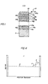
- FIG. 1 shows a p-i-n type photovoltaic device 10, such as a solar cell, made up of individual p-i-n type cells 12a, 12b, and 12c.
- a substrate 11 adjacent cell 12a forms one electrode of cell 10.
- Substrate 11 may be a metallic material such as stainless steel or aluminum, a thin electroformed member, such as nickel, or an insulating material, such as a glass or synthetic polymer, bearing an electrically conductive electrode layer. Certain applications may require a thin oxide layer and/or a series of base contacts and/or a reflecting layer be disposed on substrate 11 prior to the deposition of the semiconductor material.
- the term "substrate" includes any elements added by preliminary processing.
- Each of cells, 12a, 12b, and 12c is fabricated with an amorphous semiconductor body containing at least a silicon or germanium alloy.
- Each of the semiconductor bodies includes an n-type conductivity semiconductor layer 20a, 20b, and 20c; a graded band gap intrinsic semiconductor layer 18a, 18b and 18c; and a p-type conductivity semiconductor layer 16a, 16b and 16c.
- cell 12b is an intermediate cell and, as indicated in Figure 1, additional intermediate cells may be stacked on the illustrated cells without departing from the spirit or scope of the present invention.
- a transparent conductive oxide (TCO) layer 22 formed in the preferred embodiment of indium tin oxide, is deposited on cell 12c and forms a second electrode.
- a metallic electrode grid 24 is preferably applied to layer 22 for efficient current collection.
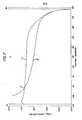
- Figure 2 is a graphical representation of hole (or electron) lifetime in the intrinsic semiconductor layer of a p-i-n photovoltaic device at various positions in that intrinsic layer.
- Curve A represents holes generated by red illumination and curve B represents holes generated by blue illumination.
- Figure 2 was derived from a computer simulation of a p-i-n photovoltaic device illuminated through the n-type layer with a flux of 10 16 photons per cm 2 . Plotted along the abscissa is the position, in microns, within the intrinsic semiconductor layer of the photovoltaic cell. The ordinate shows the logarithm of hole lifetime as measured in seconds.
- the intrinsic layer of amorphous silicon alloy material was determined to possess an absorption coefficient of 2 ⁇ 10 3 cm -1 with respect to red light.
- Curve B similarly depicts the lifetime of holes generated by the absorption of blue radiation in the intrinsic layer of amorphous silicon alloy material. The absorption coefficient for blue light was determined to be of 2 ⁇ 10 5 cm -1 .
- the coefficient of absorption of blue light in the amorphous silicon alloy material is two orders of magnitude greater than that of the red light. For this reason, most of the absorption of blue light will occur proximate (i.e. within 100 nanometers of) the light-incident surface of the intrinsic region. The absorption of red light will occur more uniformly throughout the bulk of the intrinsic layer. As a result of this differential light absorption in the intrinsic material, there is a differential distribution of holes generated by the absorption of the photons of light.
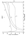
- Figure 3 is a graph of the recombination rate for holes (or electrons) at various positions in a p-i-n type photovoltaic device, for both a degraded and an undegraded semiconductor material, under both red and blue light.
- Light-induced degradation was computer simulated by increasing both the minimum density of states and the charge carrier capture cross section of the recombination centers by an order of magnitude.
- Curves-D and E respectively, represent the hole recombination rate of an undegraded photovoltaic device under red and blue illumination.
- Curves F and G respectively, represent the hole recombination rate of a degraded device under red and blue illumination.
- the undegraded device under red illumination of approximately 10 16 photons per square centimeter per second produced a soort circuit current of approximately 0.9 mA, while the degraded photovoltaic device produced a short circuit current of 0.68 mA.
- Figure 4 is a graphic representation of a p-i-n type photovoltaic device illustrating several variations in the band gap energy of the intrinsic region according to the invention.
- the band gap energy is constant throughout the intrinsic region, as indicated by dashed line H.
- the band gap energy of the intrinsic layer is graded in a uniform or stepped fashion.
- Curve J shows a smoothly varying, graded band gap intrinsic semiconductor material.
- the band gap energy of the layer of intrinsic semiconductor material represented by curve J varies linearly from a highest initial value at the n-type layer-intrinsic layer interface to a lowest value represented by the line H, at a point approximately 1/3 of the way into the bulk thickness of that intrinsic layer.
- the band gap energy may vary smoothly, in the manner illustrated by curve J, but in a non-linear manner, e.g., the variation in band gap energy with increasing thickness of the intrinsic semiconductor material may be exponential.
- the band gap of the intrinsic layer is graded in an abrupt or step manner, as illustrated by curve K.
- Curve K shows two levels of band gap energy (i.e. one step), but the band gap energy may be varied through the use of as great a number of steps as deemed convenient.
- Curves J and K depict the band gap energy as graded through only a portion of the bulk thickness of the intrinsic semiconductor layer. The entire thickness of the intrinsic layer need not be band gap graded in order to spread the absorption of blue light. It has been found that if the initial one to two hundred nanometers of the intrinsic layer is band gap graded, the desired absorption will be promoted to secure improved stability.
- Photovoltaic devices according to the invention may be manufactured by any of several known thin film deposition processes, including sputtering, evaporation, chemical vapor deposition, or glow discharge deposition.
- the improved, more stable photovoltaic device of the instant invention may be fabricated by incorporating increasing amounts of one or more band gap widening elements into the amorphous semiconductor alloy material of the intrinsic layer of a p-i-n photovoltaic device as that intrinsic layer is being deposited.
- band gap narrowing elements such as germanium, tin, lead, and mixtures thereof, may be employed to narrow the band gap of amorphous semiconductor materials such as silicon and germanium alloys.
- An embodiment of the instant invention a p-i-n type photovoltaic device, was prepared by a glow discharge deposition technique.
- a p-doped semiconductor layer less than 20 nanometers thick was deposited upon a stainless steel substrate by the glow discharge decomposition of a gas mixture comprising silane, hydrogen and diborane gas, through the application of radio frequency energy of approximately 13.56 megahertz at a gas pressure of approximately 66.7 pascal.
- the deposition chamber was purged and a process gas mixture for depositing a layer of intrinsic amorphous silicon alloy material was admitted.
- the precursor intrinsic process gas mixture comprised silane and hydrogen, and the pressure within the deposition chamber was maintained at approximately 66.7 pascal.
- the decomposition of the process gas mixture and the deposition of the intrinsic semiconductor alloy layer was initiated by the application of radio frequency energy and allowed to proceed until approximately 400 nanometers of intrinsic amorphous silicon alloy material was deposited.
- ammonia equal to 30% of the amount of silane present, was admitted into the deposition chamber and the deposition process proceeded until approximately an additional 100 nanometers of intrinsic amorphous silicon:nitrogen alloy material was deposited.
- a graded band gap structure comprising approximately 400 nanometers of an intrinsic amorphous silicon alloy material and 100 nanometers of amorphous silicon:nitrogen alloy material was deposited.
- a layer of less than approximately 20 nanometers thickness of n-doped amorphous silicon alloy material was deposited on the intrinsic semiconductor layer by the glow discharge decomposition of a process gas mixture comprising silane, hydrogen and phosphine.
- a transparent electrode formed of indium tin oxide was deposited on the layer of n-doped semiconductor alloy material in a reactive evaporation process.
- a pair of p-i-n type photovoltaic devices specifically including t nd gap graded intrinsic layers were fabricated by glow discharge deposition.
- the devices comprised an aggregate of layers formed on stainless steel substrates.
- Each aggregate of layers included an approximately 10 nanometer thick layer of p-type semiconductor material fabricated by the glow discharge decomposition of a mixture of silane and diborane; and an approximately 10 nanometer thick layer of n-type semiconductor mate-ial fabricated by the glow discharge decomposition of silane and phosphine.
- Disposed between the p-type and n-type layers is the graded band gap layer of intrinsic semiconductor material according to the invention.
- the graded band gap layer comprises a first approximately 400 nanometer thick portion formed of an amorphous silicon:hydrogen alloy having a band gap of approximately 1.7 electron volts, disposed immediately on the p-layer; and a second approximately 100 nanometer thick portion formed of an amorphous silicon:hydrogen:nitrogen alloy having a band gap of approximately 1.9 electron volts disposed on the 1.7 electron volt portion.
- Deposition of both of the band gap graded intrinsic layer portions was accomplished by a glow discharge process.
- the 1.7 electron volt portion of the intrinsic layer was deposited by the decomposition of silane, and the 1.9 electron volt portion was deposited by the decomposition of a mixture of 30 percent ammonia and 70 percent silane.
- a similar p-i-n photovoltaic device having a 500 nanometer thick, ungraded intrinsic layer of semiconductor material with a constant 1.7 electron volt band gap was prepared in an identical glow discharge deposition process.
- This particular device configuration with a relatively thick single p-i-n photovoltaic cell is known to show a high degree of photo-induced degradation.
- Initial operational parameters were measured, and the devices were then subjected to prolonged exposure to AM-1 (i.e. one sun directly overhead reduced by atmospheric losses) illumination.
- AM-1 i.e. one sun directly overhead reduced by atmospheric losses
- Short circuit current under blue illumination was measured after 6 and 72 hours of AM-1 illumination. After 6 hours of illumination, the blue light short circuit current of the test devices were 96.0 percent and 97.1 percent of the initial values, while for the control device it was 72 percent of its original value. After 72 hours, the test devices still exhibited 91.3 percent and 90.3 percent of their initial blue light short circuit currents, while the control device fell to 54 percent of its initial value.
- the invention is equally applicable to n-i-p devices illuminated on the p-doped semiconductor layer side.
- the electrons represent the minority charge carriers and therefore determine cell efficiency.
- the previous discussion relative to holes will be applicable to electrons in n-i-p devices.
- the principles of the invention may be similarly applied to other photo-responsive devices, such as p-n devices, or Schottky barrier devices, in which a photo-responsive region is formed in a semiconductor material at an interface with a metallic layer.
Landscapes
- Physics & Mathematics (AREA)
- Condensed Matter Physics & Semiconductors (AREA)
- Electromagnetism (AREA)
- General Physics & Mathematics (AREA)
- Engineering & Computer Science (AREA)
- Computer Hardware Design (AREA)
- Microelectronics & Electronic Packaging (AREA)
- Power Engineering (AREA)
- Photovoltaic Devices (AREA)
Abstract
An amorphous semiconductor photovoltaic device having improved long term efficiency stability. The improved stability is achieved by grading the band gap energy of a portion of the photo-responsive layer of the device. The widest band gap energy portion of the photo-responsive layer is disposed nearest the light-incident surface of the device. The band gap gradation may be smooth or stepped, and may be accomplished by varying the composition of the source materials during deposition of the photo-responsive layer.
Description
- Thin film amorphous semiconductor materials offer several distinct advantage over crystalline materials. Amorphous semiconductors can be easily and economically fabricated into large-area photoresponsive devices by newly developed mass production processes. However, photoresponsive amorphous silicon-based semiconductor materials have historically degraded in performance over time as a result of prolonged exposure to light. This process, termed "photo-induced degradation", or "Staebler-Wronski degradation," is not fully understood. Photo-induced degradation is believed to result from the formation of defect states in the band gap of the material by broken semiconductor-semiconductor bonds. The photo-induced defects may be removed by annealing at a temperature of approximately 150°C for several hours.
- The higher the quality of amorphous photovoltaic semiconductor material, the greater the degree of degrading by light. This observation is expected since lower quality amorphous photovoltaic semiconductor material includes a relatively high number of defect states and the formation of additional defect states under illumination is not as significant a change as in higher quality material which contains a lower initial defect density.
- Photovoltaic cells that comprise a layer of intrinsic amorphous semiconductor material having a layer of p-type semiconductor material disposed on one side and a layer of n-type semiconductor material disposed on the opposite side are referred to as p-i-n cells. We have observed in such cells that photo-induced degradation causes a very large decrease in blue response as compared to the decrease in the red response. That is, the efficiency measured under blue illumi-nation decreases much more than the efficiency measured under red illumination. "Blue illumination" is defined as having wavelengths from approximately 350 to 550 nanometers; "red illumination" is defined as having wavelengths from approximately 550 to 750 nanometers. It is known that blue light is absorbed in amorphous silicon alloy materials much more readily than red light. In fact, blue light is almost totally absorbed in the first hundred nanometers of the photo-active or intrinsic region of a p-i-n cell, but red light is absorbed throughout a greater volume of the intrinsic region. Blue illumination therefore produces a high density of charge carriers within a shal'ow volume of the intrinsic region. The high density of carriers encourages recombination and decreases photocell efficiency, much like a high concentration of defect states in a degraded photovoltaic cell decreases efficiency.
- In the invention, the problem of photo-induced degradation of amorphous semiconductor photovoltaic cells is attacked by changing the depth in the intrinsic region at which charge carriers are produced by blue illumination. The invention provides that blue light is absorbed throughout the intrinsic region, much as red light is, to discourage recombination either from a high density of light-generated charge carriers or from defects produced by prolonged illumination.
- Light passing through a homogenous solid decreases in intensity at an exponential rate. In the invention, the solid, the photovoltaic cell, is constructed so that light intensity decreases at less than an exponential rate in the intrinsic region of the cell. The desired result is achieved by grading the band gap of the intrinsic layer of the photovoltaic cell. That is, the band gap energy of the layer varies spatially in the direction of light penetration. A relatively wide band gap energy region (for instance 1.9eV) is provided proximate the light incident surface of the intrinsic region and a narrower band gap energy region (for instance 1.7eV) is provided deeper in the region. The band gap energy grading includes smooth variations, abrupt, stepped variations and any combination of smooth and abrupt variations. The grading of the band gap energy of the intrinsic layer of a p-i-n type photovoltaic devices results in absorption of blue light throughout a substantial portion of the bulk of the intrinsic region and an increase of the effective lifetime of photo-generated charge carriers. The improved photovoltaic cells exhibit increased tolerance to defect states, that is to photo-induced degradation. It is not necessary to grade the entire layer of intrinsic material.
-
- Figure is a fragmentary, cross-sectional view of a multiple cell p-i-n photovoltaic device.
- Figure 2 is a graph of the lifetime of holes generated by the absorption of blue and red illumination in the intrinsic semiconductor layer of a p-i-n photovoltaic device plotted as a function of position within the device.
- Figure 3 is a graph of the recombination rate for holes (or electrons) generated by the absorption of blue and red illumination in the intrinsic semiconductor layer of both a degraded and a undegraded p-i-n photovoltaic device as a function of position within the device.
- Figure 4 is a graph of the band gap energy of the intrinsic semiconductor material of a p-i-n type photovoltaic device as a function of the thickness of that layer, according to various embodiments of the invention.
- Figure 1 shows a p-i-n type
photovoltaic device 10, such as a solar cell, made up of individualp-i-n type cells cell 10. Substrate 11 may be a metallic material such as stainless steel or aluminum, a thin electroformed member, such as nickel, or an insulating material, such as a glass or synthetic polymer, bearing an electrically conductive electrode layer. Certain applications may require a thin oxide layer and/or a series of base contacts and/or a reflecting layer be disposed on substrate 11 prior to the deposition of the semiconductor material. As used here, the term "substrate" includes any elements added by preliminary processing. - Each of cells, 12a, 12b, and 12c is fabricated with an amorphous semiconductor body containing at least a silicon or germanium alloy. Each of the semiconductor bodies includes an n-type
conductivity semiconductor layer intrinsic semiconductor layer conductivity semiconductor layer 16a, 16b and 16c. As illustrated,cell 12b is an intermediate cell and, as indicated in Figure 1, additional intermediate cells may be stacked on the illustrated cells without departing from the spirit or scope of the present invention. - A transparent conductive oxide (TCO)
layer 22, formed in the preferred embodiment of indium tin oxide, is deposited oncell 12c and forms a second electrode. Ametallic electrode grid 24 is preferably applied tolayer 22 for efficient current collection. - Recombination of charge carriers is a major factor in determining the losses in the conversion efficiency of photovoltaic devices. In p-i-n type photovoltaic cells, it has been found that the recombination of charge carriers near the light-incident surface of the intrinsic semiconductor is controlled by hole lifetime, since holes represent minority charge carriers in this region. Based upon laboratory observation and computer simulations of p-i-n photovoltaic devices, it has been determined that effective hole lifetime depends upon the wavelength of the incident radiation producing the holes. Red light produces holes having longer effective lifetimes than holes generated by blue light. Since the semiconductor material in amorphous silicon photovoltaic cells are typically extremely thin, bulk properties, such as characteristic carrier lifetimes are not manifested. Therefore, it is correct to speak of "effective carrier lifetimes" when discussing charge carriers in such photovoltaic cells.
- Figure 2 is a graphical representation of hole (or electron) lifetime in the intrinsic semiconductor layer of a p-i-n photovoltaic device at various positions in that intrinsic layer. Curve A represents holes generated by red illumination and curve B represents holes generated by blue illumination. Figure 2 was derived from a computer simulation of a p-i-n photovoltaic device illuminated through the n-type layer with a flux of 1016 photons per cm2. Plotted along the abscissa is the position, in microns, within the intrinsic semiconductor layer of the photovoltaic cell. The ordinate shows the logarithm of hole lifetime as measured in seconds. The intrinsic layer of amorphous silicon alloy material was determined to possess an absorption coefficient of 2×103cm-1 with respect to red light. Curve B similarly depicts the lifetime of holes generated by the absorption of blue radiation in the intrinsic layer of amorphous silicon alloy material. The absorption coefficient for blue light was determined to be of 2×105cm-1.
- The coefficient of absorption of blue light in the amorphous silicon alloy material is two orders of magnitude greater than that of the red light. For this reason, most of the absorption of blue light will occur proximate (i.e. within 100 nanometers of) the light-incident surface of the intrinsic region. The absorption of red light will occur more uniformly throughout the bulk of the intrinsic layer. As a result of this differential light absorption in the intrinsic material, there is a differential distribution of holes generated by the absorption of the photons of light.
- If the absorption characteristics of the intrinsic layer for blue light could more closely approximate the absorption characteristics of red light, the effective lifetimes of holes generated by red and blue light would be about the same. If those effective lifetimes are about the same, a lower loss in efficiency upon photo-induced degradation will occur. '
- Figure 3 is a graph of the recombination rate for holes (or electrons) at various positions in a p-i-n type photovoltaic device, for both a degraded and an undegraded semiconductor material, under both red and blue light. Light-induced degradation was computer simulated by increasing both the minimum density of states and the charge carrier capture cross section of the recombination centers by an order of magnitude. Curves-D and E, respectively, represent the hole recombination rate of an undegraded photovoltaic device under red and blue illumination. Curves F and G, respectively, represent the hole recombination rate of a degraded device under red and blue illumination. The lowest hole recombination rate, exhibited by the undegraded device under red illumination, is relatively uniform throughout the thickness of the intrinsic layer, neglecting variations due to interface defects which occur in the immediate proximity of the interfaces between the intrinsic and doped layers. Even after light-induced degradation, the rate of hole recombination under red illumination remains relatively uniform and relatively low. The undegraded device under red illumination of approximately 1016 photons per square centimeter per second produced a soort circuit current of approximately 0.9 mA, while the degraded photovoltaic device produced a short circuit current of 0.68 mA.
- While the rate of hole recombination is relatively high in the undegraded device (curve E) the rate of hole recombination is much higher after degradation (curve G). Therefore, the rate of recombination for blue generated charge carriers varies greatly throughout the intrinsic layer, with the highest rate of hole recombination occuring in the first third of the intrinsic layer. This high hole recombination rate is reflected in the photo-induced loss of efficiency. The undegraded device represented by curve E generates a short circuit current of 1.14 mA upon illumination with a flux of 1016 photons per square centimeter per second, but the photo-induced degraded device generates a short circuit current of only 0.11 mA under the same conditions. This difference represents a 90 percent loss in efficiency.
- In curves D through G, the loss in efficiency of the device upon photo-induced degradation is primarily due to the loss of blue response. That loss is most severe in approximately the first one hundred nanometers of the tight-incident side of the layer of intrinsic material and correlates to the higher absorption of blue light as compared to absorption of red light.
- In our invention, uniform absorption of both blue and red light is promoted by grading the band gap energy of the semiconductor material that forms the intrinsic layer. Incident light is absorbed more deeply in the bulk thickness of the intrinsic region of the device avoiding the formation of a high density of charge carriers proximate the light-incident surface. In other words, stability of the photovoltaic device is increased by distributing charge carriers more uniformly throughout the bulk thickness of the intrinsic region.
- Figure 4 is a graphic representation of a p-i-n type photovoltaic device illustrating several variations in the band gap energy of the intrinsic region according to the invention. In prior art photovoltaic devices, the band gap energy is constant throughout the intrinsic region, as indicated by dashed line H. In the invention, the band gap energy of the intrinsic layer is graded in a uniform or stepped fashion. Curve J shows a smoothly varying, graded band gap intrinsic semiconductor material. The band gap energy of the layer of intrinsic semiconductor material represented by curve J, varies linearly from a highest initial value at the n-type layer-intrinsic layer interface to a lowest value represented by the line H, at a point approximately 1/3 of the way into the bulk thickness of that intrinsic layer. In an alternative embodiment, rot illustrated, the band gap energy may vary smoothly, in the manner illustrated by curve J, but in a non-linear manner, e.g., the variation in band gap energy with increasing thickness of the intrinsic semiconductor material may be exponential.
- In another embodiment of the invention, the band gap of the intrinsic layer is graded in an abrupt or step manner, as illustrated by curve K. Curve K shows two levels of band gap energy (i.e. one step), but the band gap energy may be varied through the use of as great a number of steps as deemed convenient. Curves J and K depict the band gap energy as graded through only a portion of the bulk thickness of the intrinsic semiconductor layer. The entire thickness of the intrinsic layer need not be band gap graded in order to spread the absorption of blue light. It has been found that if the initial one to two hundred nanometers of the intrinsic layer is band gap graded, the desired absorption will be promoted to secure improved stability.
- Photovoltaic devices according to the invention may be manufactured by any of several known thin film deposition processes, including sputtering, evaporation, chemical vapor deposition, or glow discharge deposition.
- Certain elements, including nitrogen, oxygen, fluorine and carbon, whether taken alone or in combination, are capable of widening the band gap of amorphous silicon and germanium alloy materials. Accordingly, the improved, more stable photovoltaic device of the instant invention may be fabricated by incorporating increasing amounts of one or more band gap widening elements into the amorphous semiconductor alloy material of the intrinsic layer of a p-i-n photovoltaic device as that intrinsic layer is being deposited. Alternatively, band gap narrowing elements, such as germanium, tin, lead, and mixtures thereof, may be employed to narrow the band gap of amorphous semiconductor materials such as silicon and germanium alloys. By utilizing this approach to band gap grading, decreasing amounts of band gap narrowing elements are added to the intrinsic layer of semiconductor material as it is deposited.
- An embodiment of the instant invention, a p-i-n type photovoltaic device, was prepared by a glow discharge deposition technique. A p-doped semiconductor layer less than 20 nanometers thick was deposited upon a stainless steel substrate by the glow discharge decomposition of a gas mixture comprising silane, hydrogen and diborane gas, through the application of radio frequency energy of approximately 13.56 megahertz at a gas pressure of approximately 66.7 pascal. Upon completion of the deposition of the p-doped layer, the deposition chamber was purged and a process gas mixture for depositing a layer of intrinsic amorphous silicon alloy material was admitted. The precursor intrinsic process gas mixture comprised silane and hydrogen, and the pressure within the deposition chamber was maintained at approximately 66.7 pascal. The decomposition of the process gas mixture and the deposition of the intrinsic semiconductor alloy layer was initiated by the application of radio frequency energy and allowed to proceed until approximately 400 nanometers of intrinsic amorphous silicon alloy material was deposited. At that time, ammonia, equal to 30% of the amount of silane present, was admitted into the deposition chamber and the deposition process proceeded until approximately an additional 100 nanometers of intrinsic amorphous silicon:nitrogen alloy material was deposited. In this manner, a graded band gap structure comprising approximately 400 nanometers of an intrinsic amorphous silicon alloy material and 100 nanometers of amorphous silicon:nitrogen alloy material was deposited. Following the deposition of the graded intrinsic semiconductor layer, a layer of less than approximately 20 nanometers thickness of n-doped amorphous silicon alloy material was deposited on the intrinsic semiconductor layer by the glow discharge decomposition of a process gas mixture comprising silane, hydrogen and phosphine. In a subsequent processing step, a transparent electrode formed of indium tin oxide was deposited on the layer of n-doped semiconductor alloy material in a reactive evaporation process.
- A pair of p-i-n type photovoltaic devices specifically including t nd gap graded intrinsic layers were fabricated by glow discharge deposition. The devices comprised an aggregate of layers formed on stainless steel substrates. Each aggregate of layers included an approximately 10 nanometer thick layer of p-type semiconductor material fabricated by the glow discharge decomposition of a mixture of silane and diborane; and an approximately 10 nanometer thick layer of n-type semiconductor mate-ial fabricated by the glow discharge decomposition of silane and phosphine. Disposed between the p-type and n-type layers is the graded band gap layer of intrinsic semiconductor material according to the invention. The graded band gap layer comprises a first approximately 400 nanometer thick portion formed of an amorphous silicon:hydrogen alloy having a band gap of approximately 1.7 electron volts, disposed immediately on the p-layer; and a second approximately 100 nanometer thick portion formed of an amorphous silicon:hydrogen:nitrogen alloy having a band gap of approximately 1.9 electron volts disposed on the 1.7 electron volt portion. Deposition of both of the band gap graded intrinsic layer portions was accomplished by a glow discharge process. The 1.7 electron volt portion of the intrinsic layer was deposited by the decomposition of silane, and the 1.9 electron volt portion was deposited by the decomposition of a mixture of 30 percent ammonia and 70 percent silane. For purposes of comparison and control, a similar p-i-n photovoltaic device having a 500 nanometer thick, ungraded intrinsic layer of semiconductor material with a constant 1.7 electron volt band gap was prepared in an identical glow discharge deposition process.
- This particular device configuration with a relatively thick single p-i-n photovoltaic cell is known to show a high degree of photo-induced degradation. Initial operational parameters were measured, and the devices were then subjected to prolonged exposure to AM-1 (i.e. one sun directly overhead reduced by atmospheric losses) illumination. Short circuit current under blue illumination was measured after 6 and 72 hours of AM-1 illumination. After 6 hours of illumination, the blue light short circuit current of the test devices were 96.0 percent and 97.1 percent of the initial values, while for the control device it was 72 percent of its original value. After 72 hours, the test devices still exhibited 91.3 percent and 90.3 percent of their initial blue light short circuit currents, while the control device fell to 54 percent of its initial value.
- While the foregoing description has dealt primarily with p-i-n type photovoltaic devices, the invention is equally applicable to n-i-p devices illuminated on the p-doped semiconductor layer side. In such devices the electrons represent the minority charge carriers and therefore determine cell efficiency. Accordingly, the previous discussion relative to holes will be applicable to electrons in n-i-p devices. The principles of the invention may be similarly applied to other photo-responsive devices, such as p-n devices, or Schottky barrier devices, in which a photo-responsive region is formed in a semiconductor material at an interface with a metallic layer.
Claims (15)
1. An improved amorphous semiconductor photovoltaic device (10) having a light-incident surface and at least one set (12a) of successive layers beneath said surface for receiving light and generating charge carriers in response to said light, said set including a p-type layer (20a), an adjacent intrinsic layer (18a) and an n-type layer (16a) adjacent to said intrinsic layer (18a) opposite said p-type region (20a) characterized in that said intrinsic layer (18a) includes a graded band gap energy through a portion of said region, the widest band gap energy being disposed in said intrinsic layer nearest said light-incident surface.
2. The device of claim 1 characterized in that the intrinsic layer (18a) includes a gradient of band gap energy reducing material.
3. The device of claim 2 characterized in that said band gap energy reducing material is chosen from the group consisting essentially of germanium, tin, lead and mixtures thereof.
4. The device of claim 1 characterized in that the intrinsic layer (18a) includes a gradient of band gap energy increasing material.
5. The device of claim 4 characterized in that the band gap energy increasing material is chosen from the group consisting essentially of nitrogen, oxygen, carbon,, fluorine and mixtures thereof.
6. The device of claim 1 characterized in that the widest band gap portion of the intrinsic region (18a) has a band gap energy of approximately 1.8 to 2.1 electron volts and the narrowest gap portion has a band gap energy of approximately 1.5 to 1.8 electron volts.
7. The photovoltaic device of claim 1 characterized in that the band gap energy of the intrinsic layer (18a) is smoothly graded.
8. The device of claim 1 characterized in that the band gap energy of the intrinsic layer is graded in an abrupt step.
9. A method of producing an improved amorphous semiconductor photovoltaic device having a light-incident surface and at least one set of successively deposited layers disposed beneath said surface for receiving light and generating charge carriers in response to said light, said method including depositing a n-type layer, depositing an intrinsic layer on said n-type layer and depositing a p-type layer on said intrinsic layer opposite said n-type layer, characterized in that a portion of said intrinsic layer is co-deposited with a band gap energy altering material to grade the band gap energy of said intrinsic layer, the widest band gap energy being disposed in said intrinsic layer nearest said light-incident surface.
10. The method of claim 9 characterized in that said band gap energy altering material is a band gap energy reducing material.
11. The method of claim 10 characterized in that said band gap energy reducing material is chosen from the group consisting essentially of germanium, tin, lead and mixtures thereof.
12. The method of claim 9 characterized in that said band gap energy altering material is a. band gap energy increasing material.
13. The method of claim 12 characterized in that the band gap energy increasing material is chosen from the group consisting essentially of nitrogen, oxygen, carbon, fluorine and mixtures thereof.
14. The method of claim 9 charterized in that the amount of said band gap energy altering material co-deposited with said intrinsic layer is gradually changed during the deposition of said intrinsic layer.
15. The method of claim 9 charterized in that the amount of said band gap energy altering material co-deposited with said intrinsic layer is abruptly changed during the deposition of said intrinsic layer.
Applications Claiming Priority (2)
| Application Number | Priority Date | Filing Date | Title |
|---|---|---|---|
| US623860 | 1984-06-25 | ||
| US06/623,860 US4547621A (en) | 1984-06-25 | 1984-06-25 | Stable photovoltaic devices and method of producing same |
Publications (2)
| Publication Number | Publication Date |
|---|---|
| EP0167323A2 true EP0167323A2 (en) | 1986-01-08 |
| EP0167323A3 EP0167323A3 (en) | 1986-07-16 |
Family
ID=24499680
Family Applications (1)
| Application Number | Title | Priority Date | Filing Date |
|---|---|---|---|
| EP85304351A Withdrawn EP0167323A3 (en) | 1984-06-25 | 1985-06-18 | Stable photovoltaic devices and method of producing same |
Country Status (9)
| Country | Link |
|---|---|
| US (1) | US4547621A (en) |
| EP (1) | EP0167323A3 (en) |
| JP (1) | JPH0671090B2 (en) |
| AU (1) | AU4399585A (en) |
| BR (1) | BR8503017A (en) |
| CA (1) | CA1262766A (en) |
| ES (1) | ES8609820A1 (en) |
| MX (1) | MX157839A (en) |
| ZA (1) | ZA854621B (en) |
Families Citing this family (17)
| Publication number | Priority date | Publication date | Assignee | Title |
|---|---|---|---|---|
| US4692558A (en) * | 1983-05-11 | 1987-09-08 | Chronar Corporation | Counteraction of semiconductor impurity effects |
| US4772933A (en) * | 1986-02-03 | 1988-09-20 | General Electric Company | Method for compensating operationally-induced defects and semiconductor device made thereby |
| JPS62234379A (en) * | 1986-04-04 | 1987-10-14 | Kanegafuchi Chem Ind Co Ltd | Semiconductor device |
| JP2717583B2 (en) * | 1988-11-04 | 1998-02-18 | キヤノン株式会社 | Stacked photovoltaic element |
| US5204272A (en) * | 1991-12-13 | 1993-04-20 | United Solar Systems Corporation | Semiconductor device and microwave process for its manufacture |
| AU2003269667A1 (en) * | 2002-10-25 | 2004-05-13 | Unaxis Balzers Ltd. | Method for producing semi-conducting devices and devices obtained with this method |
| EP2140482A2 (en) * | 2006-06-12 | 2010-01-06 | Matthew R. Robinson | Thin-film devices fromed from solid particles |
| JP5526461B2 (en) * | 2007-03-19 | 2014-06-18 | 三洋電機株式会社 | Photovoltaic device |
| KR101359401B1 (en) * | 2007-06-21 | 2014-02-10 | 주성엔지니어링(주) | High efficiency thin film solar cell and manufacturing method and apparatus thereof |
| US8440498B2 (en) | 2009-10-28 | 2013-05-14 | Nanosolar, Inc. | Thin-film devices formed from solid particles |
| US9634165B2 (en) * | 2009-11-02 | 2017-04-25 | International Business Machines Corporation | Regeneration method for restoring photovoltaic cell efficiency |
| US20110240121A1 (en) * | 2010-04-02 | 2011-10-06 | Iowa State University Research Foundation, Inc. | Nanocrystalline Superlattice Solar Cell |
| KR20130042785A (en) * | 2011-10-19 | 2013-04-29 | 한국전자통신연구원 | Solar cell |
| US9040340B2 (en) * | 2011-11-14 | 2015-05-26 | International Business Machines Corporation | Temperature grading for band gap engineering of photovoltaic devices |
| MX356512B (en) * | 2012-12-13 | 2018-05-30 | Daniel Scott Marshall | Magnetically polarized photonic device. |
| US9722120B2 (en) * | 2015-09-14 | 2017-08-01 | International Business Machines Corporation | Bandgap grading of CZTS solar cell |
| US10361331B2 (en) | 2017-01-18 | 2019-07-23 | International Business Machines Corporation | Photovoltaic structures having multiple absorber layers separated by a diffusion barrier |
Citations (6)
| Publication number | Priority date | Publication date | Assignee | Title |
|---|---|---|---|---|
| US4206002A (en) * | 1976-10-19 | 1980-06-03 | University Of Pittsburgh | Graded band gap multi-junction solar energy cell |
| JPS5688377A (en) * | 1979-12-19 | 1981-07-17 | Mitsubishi Electric Corp | Solar battery and manufacture thereof |
| GB2083701A (en) * | 1980-09-09 | 1982-03-24 | Energy Conversion Devices Inc | Graded bandgap amorphous semiconductors |
| US4377723A (en) * | 1980-05-02 | 1983-03-22 | The University Of Delaware | High efficiency thin-film multiple-gap photovoltaic device |
| US4379943A (en) * | 1981-12-14 | 1983-04-12 | Energy Conversion Devices, Inc. | Current enhanced photovoltaic device |
| JPS5898988A (en) * | 1981-12-08 | 1983-06-13 | Matsushita Electric Ind Co Ltd | Solar photocell |
Family Cites Families (5)
| Publication number | Priority date | Publication date | Assignee | Title |
|---|---|---|---|---|
| US4342044A (en) * | 1978-03-08 | 1982-07-27 | Energy Conversion Devices, Inc. | Method for optimizing photoresponsive amorphous alloys and devices |
| JPS58220478A (en) * | 1982-06-17 | 1983-12-22 | Matsushita Electric Ind Co Ltd | Amorphous photoelectric converting element |
| JPS5997514A (en) * | 1982-11-22 | 1984-06-05 | Agency Of Ind Science & Technol | Manufacture of amorphous silicon film |
| US4471155A (en) * | 1983-04-15 | 1984-09-11 | Energy Conversion Devices, Inc. | Narrow band gap photovoltaic devices with enhanced open circuit voltage |
| JPH0658970B2 (en) * | 1983-08-31 | 1994-08-03 | 工業技術院長 | Semiconductor device |
-
1984
- 1984-06-25 US US06/623,860 patent/US4547621A/en not_active Expired - Lifetime
-
1985
- 1985-06-18 EP EP85304351A patent/EP0167323A3/en not_active Withdrawn
- 1985-06-19 CA CA000484433A patent/CA1262766A/en not_active Expired
- 1985-06-19 ZA ZA854621A patent/ZA854621B/en unknown
- 1985-06-24 BR BR8503017A patent/BR8503017A/en unknown
- 1985-06-24 JP JP60137633A patent/JPH0671090B2/en not_active Expired - Lifetime
- 1985-06-24 AU AU43995/85A patent/AU4399585A/en not_active Abandoned
- 1985-06-24 ES ES544481A patent/ES8609820A1/en not_active Expired
- 1985-07-24 MX MX205759A patent/MX157839A/en unknown
Patent Citations (6)
| Publication number | Priority date | Publication date | Assignee | Title |
|---|---|---|---|---|
| US4206002A (en) * | 1976-10-19 | 1980-06-03 | University Of Pittsburgh | Graded band gap multi-junction solar energy cell |
| JPS5688377A (en) * | 1979-12-19 | 1981-07-17 | Mitsubishi Electric Corp | Solar battery and manufacture thereof |
| US4377723A (en) * | 1980-05-02 | 1983-03-22 | The University Of Delaware | High efficiency thin-film multiple-gap photovoltaic device |
| GB2083701A (en) * | 1980-09-09 | 1982-03-24 | Energy Conversion Devices Inc | Graded bandgap amorphous semiconductors |
| JPS5898988A (en) * | 1981-12-08 | 1983-06-13 | Matsushita Electric Ind Co Ltd | Solar photocell |
| US4379943A (en) * | 1981-12-14 | 1983-04-12 | Energy Conversion Devices, Inc. | Current enhanced photovoltaic device |
Non-Patent Citations (2)
| Title |
|---|
| PATENTS ABSTRACTS OF JAPAN, vol. 5, no. 159 (E-77) [831], 14th October 1981; & JP - A - 56 88 377 (MITSUBISHI DENKI K.K.) 17-07-1981 * |
| PATENTS ABSTRACTS OF JAPAN, vol. 7, no. 200 (E-196) [1345] 3rd September 1983; & JP - A - 58 98 988 (MATSUSHITA DENKI SANGYO K.K.) 13-06-1983 * |
Also Published As
| Publication number | Publication date |
|---|---|
| JPH0671090B2 (en) | 1994-09-07 |
| US4547621A (en) | 1985-10-15 |
| JPS6113673A (en) | 1986-01-21 |
| CA1262766A (en) | 1989-11-07 |
| EP0167323A3 (en) | 1986-07-16 |
| ES544481A0 (en) | 1986-07-16 |
| MX157839A (en) | 1988-12-15 |
| ES8609820A1 (en) | 1986-07-16 |
| ZA854621B (en) | 1986-02-26 |
| AU4399585A (en) | 1986-01-02 |
| BR8503017A (en) | 1986-03-11 |
Similar Documents
| Publication | Publication Date | Title |
|---|---|---|
| US4476346A (en) | Photovoltaic device | |
| EP0167323A2 (en) | Stable photovoltaic devices and method of producing same | |
| US5403404A (en) | Multijunction photovoltaic device and method of manufacture | |
| Carlson | Recent developments in amorphous silicon solar cells | |
| US4775425A (en) | P and n-type microcrystalline semiconductor alloy material including band gap widening elements, devices utilizing same | |
| KR960015529B1 (en) | Thin film sola cell including a spatially modulated intrinsic layer | |
| JP2006080557A (en) | Improved stabilizing properties of amorphous silicon series element manufactured by high hydrogen dilution low temperature plasma vapor deposition | |
| US4609771A (en) | Tandem junction solar cell devices incorporating improved microcrystalline p-doped semiconductor alloy material | |
| US4600801A (en) | Fluorinated, p-doped microcrystalline silicon semiconductor alloy material | |
| US5114498A (en) | Photovoltaic device | |
| US4398054A (en) | Compensated amorphous silicon solar cell incorporating an insulating layer | |
| US5419783A (en) | Photovoltaic device and manufacturing method therefor | |
| US4555586A (en) | Photovoltiac device having long term energy conversion stability and method of producing same | |
| US5104455A (en) | Amorphous semiconductor solar cell | |
| JP3519543B2 (en) | Precursor for forming semiconductor thin film and method for producing semiconductor thin film | |
| Carlson | Solar cells | |
| KR20130061346A (en) | Solar cell and method of manufacturing the same | |
| JPS6225275B2 (en) | ||
| TWI483405B (en) | Photovoltaic cell and method of manufacturing a photovoltaic cell | |
| Von Roedern et al. | An Assessment of a-SiGe: H Alloys with a Band GaP of 1.5 Ev as to their Suitability for Solar Cell Applications | |
| Carlson | Photovoltaics V: amorphous silicon cells: A highly homogeneous amorphous semiconductor material promises low-cost solar cells | |
| AU2022429985A1 (en) | Solar cell and method for forming the same | |
| Call | Optimization of contaminated oxide inversion layer solar cell. Final report | |
| Chopra et al. | Amorphous silicon solar cells | |
| Hovel | Amorphous-crystalline tandem solar cell |
Legal Events
| Date | Code | Title | Description |
|---|---|---|---|
| PUAI | Public reference made under article 153(3) epc to a published international application that has entered the european phase |
Free format text: ORIGINAL CODE: 0009012 |
|
| AK | Designated contracting states |
Designated state(s): CH DE FR GB IT LI NL |
|
| PUAL | Search report despatched |
Free format text: ORIGINAL CODE: 0009013 |
|
| AK | Designated contracting states |
Kind code of ref document: A3 Designated state(s): CH DE FR GB IT LI NL |
|
| STAA | Information on the status of an ep patent application or granted ep patent |
Free format text: STATUS: THE APPLICATION IS DEEMED TO BE WITHDRAWN |
|
| 18D | Application deemed to be withdrawn |
Effective date: 19870119 |
|
| RIN1 | Information on inventor provided before grant (corrected) |
Inventor name: HACK, MICHAEL Inventor name: GUHA, SUBHENDU |