EP0166192A2 - High-speed buffer store arrangement for fast transfer of data - Google Patents
High-speed buffer store arrangement for fast transfer of data Download PDFInfo
- Publication number
- EP0166192A2 EP0166192A2 EP85106189A EP85106189A EP0166192A2 EP 0166192 A2 EP0166192 A2 EP 0166192A2 EP 85106189 A EP85106189 A EP 85106189A EP 85106189 A EP85106189 A EP 85106189A EP 0166192 A2 EP0166192 A2 EP 0166192A2
- Authority
- EP
- European Patent Office
- Prior art keywords
- cache
- latches
- data
- storage
- read
- Prior art date
- Legal status (The legal status is an assumption and is not a legal conclusion. Google has not performed a legal analysis and makes no representation as to the accuracy of the status listed.)
- Granted
Links
Images


Classifications
-
- G—PHYSICS
- G06—COMPUTING; CALCULATING OR COUNTING
- G06F—ELECTRIC DIGITAL DATA PROCESSING
- G06F12/00—Accessing, addressing or allocating within memory systems or architectures
- G06F12/02—Addressing or allocation; Relocation
- G06F12/08—Addressing or allocation; Relocation in hierarchically structured memory systems, e.g. virtual memory systems
- G06F12/0802—Addressing of a memory level in which the access to the desired data or data block requires associative addressing means, e.g. caches
- G06F12/0893—Caches characterised by their organisation or structure
- G06F12/0897—Caches characterised by their organisation or structure with two or more cache hierarchy levels
Definitions
- This invention is concerned with high-speed buffer stores or caches in data processing systems, and in particular with the design and interconnection of multiple caches to enable fast transfer of data sets between the caches, and also between a cache and the main store or processing unit.
- U.S. Patent 4,141,067 discloses a multiprocessor system in which each CPU has its own cache store. Separate latches are provided between each cache store and its CPU to buffer data. No transfer or interaction between the several caches is provided, as each cache serves its own processor.
- a parallel processor having a large number of elementary processors connected in parallel.
- Each elementary processor has its own normal storage unit and its own small capacity fast storage unit. These fast storage units are interconnected to allow the desired parallel processing. However, no transfer of separate data sets between the fast stores or between a selectable fast store and a single common main store are provided.
- U.S. Patent 4,228,503 describes a multi-requestor system in which each requestor has its own dedicated cache store. Besides having access to its own cache store for obtaining data, each requestor also has access to all other dedicated cache stores for inva- lidating a particular data word therein if that same data word has been written by that requestor into its own dedicated cache store. However, a requestor cannot obtain data from another cache which is not its own, and no data transfers between caches are provided.
- a further object is to provide a multiple cache buffer system that allows fast transfer of data blocks to and from caches having different access times without the requirement of extra operating cycles for intermediate handling.
- the new cache buffer arrangement allows transfer of very large data blocks between storage units within one operation cycle. It is particularly suited for a hierarchical system of high-speed buffers having different speeds and sizes.
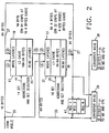
- Fig. 1 is a block diagram of the storage system which will be disclosed as an embodiment of the invention.
- a processor 11 is connected to main storage unit 13 by a storage control unit 15.
- Two cache high speed buffer stores 17 and 19 are provided to improve the availability of operands and instructions to the processor.
- the arrangement of the caches in a two-level hierarchy brought further improvement, as was e.g. explained in above-mentioned IBM Technical Disclosure Bulletin article by F.J. Sparacio.
- Cache controls 21 (L1 CTL) and 23 (L2 CTL) are provided for the two cache stores, respectively, and are connected to main storage control unit 15.
- Present invention is concerned with the internal organization of the cache buffer stores and their interconnections.
- the level 1 (L1) cache 17 has a capacity of 64 K bytes
- the level 2 (L2) cache 19 has a capacity of 1M bytes, i.e. L2 is sixteen times as large as L1.
- Data can be transferred from the main store via 16-byte wide bus 25 to the inputs of both cache buffers.
- L1 cache 17 data can be transferred via 64-byte wide bus 27 to a second input of L2 cache 19, and also through a converter 29 to a 16-byte wide bus 31 which is connected to the processor 11 and also through the storage control to main store 13.
- From L2 cache 19, data can be transferred via 64-byte wide bus 33 to a second input of L1 cache 17, and also through the converter 29 and 16-byte bus 31 to the processor and to the main store.
- bus width and storage sizes of this preferred embodiment are of course only one possibility. Other widths and sizes can be selected, depending on the design and application of the respective data processing system.
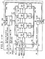
- Level 1 cache 17 with its capacity of 64 K bytes can hold 1024 (or 1K) lines of 64 bytes each. To select one line location for reading or writing 64 bytes, the cache needs the equivalent of 10 bits which are provided on a group of selection lines 35. Some of these selection bits are used for selecting a set (or subdivision) of the cache, and the others are used for addressing a specific location within the set. This will be explained in more detail in connection with Fig. 3.
- L1 cache 17 is arranged on 32 integrated circuit chips, each holding four sets of 256 double bytes (as will be shown in more detail in Fig. 3). Of any stored line of 64 bytes, each chip holds one double byte. Thus, on each of the 32 chips, there are integrated write latches 37 for one double byte (18 bits) and also read latches 39 for one double byte (18 bits).
- the access time of L1 cache chip is in the order of 3 ns or less.
- Level 2 cache 19 is of similar but not identical design as L1. With its capacity of 1 M byte it can hold 16,384 (16 K) lines of 64 bytes each. For selecting any one of these lines, the equivalent of 14 selection bits are required which are provided on selection lines 41. Details of selection and addressing in L2 cache 19 will be explained in connection with Fig. 4.
- L2 cache 19 also has a set of write latches 43 which can hold one line of 64 data bytes. These latches are selectively loaded either from L1 cache via bus 27 (input A") or from main store in four sequential passes via bus 25 (input A) like the L1 cache. L2 cache 19 also has read latches 45 which can hold a line of 64 data bytes. Contents of these latches is furnished to bus 33 (output B).
- L2 cache 19 is arranged in 64 integrated circuit chips, each holding 16 K single bytes (grouped in sets and subsets, as will be shown in more detail in Fig. 4). Of any stored line of 64 bytes, each chip holds one single byte. Thus, on each of the 64 chips, there are integrated write latches 43 for one byte (9 bits) and also read latches 45 for one byte (9 bits).
- the access time of L2 cache chip 19 is in the order of 20 ns (or less), i.e. much longer as that of Ll cache 17 because of the larger size.
- Converter 29 receives a 64-byte line from either L1 or L2, and releases it in four successive cycles in 16- byte portions (or sublines) to main store or processor.
- Block 47 in Fig. 2 represents an array of N registers which each can hold a 64-byte line which was transferred to converter 29 from either L1 cache or L2 cache. These registers allow to re-use lines of data without accessing again the respective cache high-speed buffer store. The registers feed a second 64:16 converter 30 to allow parallel cache and register readout.
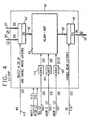
- This L1 chip 51 comprises four arrays 53, 55, 57, 59 each for storing 256 double bytes (i.e. 256 x 18 bits). It further comprises write latches 37' for storing one double byte (18 bits), and read latches 39' for storing one double byte (18 bits). The 18 bits of write latches 37' are transferred via bus 61 to all four arrays, and bus 63 is provided to transfer 18 bits from any array to read latches 39'. Write and read latches are connected to external buses 25' (input A), 33' (input A'), and 27' (output D), respectively, as was shown in Fig. 2. (Of the total 64-byte capacity of each external bus, only two bytes, i.e. 18 bits are connected to each individual chip 51, as is indicated by the stroke in 25' etc.).
- An extra feedback connection 65 is provided on the chip for transferring a double byte from read latches 39' back to write latches 37', thus forming a third input AI to the write latches.
- address bits For selecting any one of the 256 double bytes on each array, eight address bits (ADDR L1) are provided on lines 67 and are decoded in decoding circuitry 69.
- two selection bits For selecting any one of the four arrays 53, 55, 57, 59, two selection bits (SEL L1) are provided on line 71 and are decoded in decoding circuitry 73 or 74, respectively.
- the clock signal and the write enabling signal (WRITE L1) on lines 75 are used for array control and timing during a write array operation.
- WRITE L1 write enabling signal
- the selection is effected by an output signal of decoder 74 which receives the two array selection bits (SEL Ll) on lines 71 and which is enabled by a read enabling signal (READ L1) provided on line 77.
- the signal on line 77 is also used for array control.
- a two-bit control signal "W1" is provided on lines 79 for selecting any one of the inputs A, A' and AI and for enabling write latches 37' to store the two bytes available on the selected input bus.
- a further two-bit control signal "WH" is provided on lines 81 to gate either only the left byte or only the right byte of the two bytes available on the selected input bus, into write latches 37'. This enables selection of individual bytes, or the assembling of two bytes from different sources in a single byte pair.
- a read control signal "R1" is provided on single-bit line 83 to read latches 39'. This signal when active enables read latches 39' to store the double byte currently available on bus 63, as read from one of the four storage arrays.
- Control signals Wl, WH and R1 (which are furnished by L1 controls 21) are an important feature of the disclosed storage system. They enable to separate internal operation of the chips/cache from external data transfers. Thus, despite different operating speeds or access times of caches L1 and L2 and the main store, direct transfers between the different storage levels are possible with a minimum delay, i.e. without requesting extra storage cycles.
- This L2 chip 91 comprises a large array 93 of 16,384 (16 K) byte positions each holding nine data bits. It further comprises write latches 43' for storing one byte (9 bits) and read latches 45' for storing one byte (9 bits). Bus 95 connects the write latches to array 93, and bus 97 connects the array 93 to the read latches. Write and read latches are connected to external busses 25' (input A), 27' (input A"), and 33' (output B), respectively, as was shown in FIG. 2. (Of the total 64-byte capacity of each external bus, only one byte, i.e. nine bits are connected to each individual chip 91 as is indicated by the stroke in 25' etc.)
- Additional lines 113 and 115 are provided for furnishing a write enabling signal (WRITE L2) and a read enabling signal (READ L2), respectively, to storage array 93.
- WRITE L2 write enabling signal
- READ L2 read enabling signal
- a two-bit control signal "W2" is provided to write latches 43' on lines 117 for selecting one of the two inputs A and A" and for enabling write latches 43' to store the single byte available on the selected input bus.
- a read control signal "R2" is provided to read latches 45 on single-bit line 119.
- This signal when active enables read latches 45' to store the single byte currently available on bus 97 as read from storage array 93.
- Control signals W2 and R2 are an important feature of the disclosed storage system, in connection with the on-chip write and read latches, because these features significantly enhance the inter-level transfer capabilities of the cache storage hierarchy (as was already mentioned at the end of the previous section).
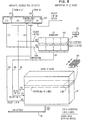
- FIG. 5 illustrates how the addressing/selection signals for level 1 cache buffer store 17 are developed from a given address.
- the 27 bits of a virtual address are stored in register 121.
- the lowest-order 6 bits are used for selecting one byte of a 64-byte line read from the L1 cache. All other bits are used for addressing one 64-byte line in cache.
- a directory look-aside table (DLAT) 123 is provided for storing recently translated addresses, as is well-known in virtual storage systems.
- the DLAT is subdivided into 256 congruence classes. All virtual addresses in which bits 7...14 are identical form one congruence class, or associative set. Thus, these eight bits are used to select the respective congruence class (or row) in the DLAT.
- Each congruence class has two entries 125, each of them storing a "STO" address field (17 bits), a virtual address field (7 bits) and the corresponding translated absolute address field (15 bits).
- the seventeen bits of a given "STO" address and the seven highest-order bits 0...6 of the virtual address register are compared with the respective fields in the two DLAT entries. If no match occurs, a translation must be made and entered into DLAT. If a match occurs, the respective translated fifteen absolute address bits are furnished at the DLAT output.
- congruence classes are used which are different from the DLAT congruence classes.
- all virtual addresses in which bits 13...20 are identical form one congruence class or associative set. These eight bits are transferred to L1 directory 127 and L1 cache 17 for selecting one congruence class (or row) of 256.
- the directory as well as the cache are 4-set associative, i.e. they have four entries per congruence class or row. In the directory, each entry 129 holds a 15-bit absolute address; in the cache, each entry 131 holds a whole data line of 64 bytes.
- the fiveteen address bits furnished by the DLAT are compared in the L1 directory with all four entries of the selected row. If no match occurs (cache miss), the respective line must be fetched to cache and the address entered into the directory. If a match occurs (cache hit), a two-bit signal identifying the respective set (column) is transferred to the Ll cache for selecting there the corresponding set (column).
- the eight addressing bits and the two set selection bits are available on lines 67 and 71 of the cache, respectively, and can be used for selecting a double byte on each of the 32 cache chips, as was explained in connection with FIG. 3.
- the 64-byte line is then stored in the read latches of all chips, and becomes available on output bus 27.
- FIG. 6 shows how the addressing/selection signals for level 2 cache buffer store 19 are developed from a given address. It is assumed that the virtual address was already translated into a 27-bit absolute address which is stored in a register 133. The twelve low-order bits 15...26 are taken directly from the virtual address whereas the 15 high-order bits 0...14 are obtained from a directory look-aside table DLAT, as was explained for L1 cache in connection with FIG. 5.
- the six lowest-order bits 21...26 of the absolute address are used for selecting one byte of a 64-byte line read from the L2 cache. All other bits (0...20) are used for addressing one 64-byte line in cache.
- the level 2 cache and its directory are also subdivided into congruence classes.
- the nine bits 7...15 of the absolute address determine the congruence class so that 512 classes can be distinguished.
- Addressing of a superline is as follows: The nine bits (7...15) determining the congruence class select one row in the L2 directory. Nine further bits of the absolute address (bits 0...6 and 16 and 17) which identify the superline (8 lines) are furnished to the directory and are compared with the four 9-bit entries in the selected row. If no match occurs (cache miss), a fetch in main store must be made and the directory updated. If a match occurs (cache hit), then the respective column is identified by a bit pair furnished at the output of L2 directory 135. This bit pair determines where within the respective congruence class the addressed superline is located in cache.
- L2 cache 19 receives the nine bits determining the congruence class (which could be designated as "row” in cache) on lines 101, and it receives the four bits determining the set or superline within that congruence class (or row) on lines 105.
Abstract
Description
- This invention is concerned with high-speed buffer stores or caches in data processing systems, and in particular with the design and interconnection of multiple caches to enable fast transfer of data sets between the caches, and also between a cache and the main store or processing unit.
- The use of high-speed buffer stores, often called "caches", for improving the operation of data processing systems is well established in the art. Several systems are known in which a plurality of caches are provided.
- U.S. Patent 4,141,067 discloses a multiprocessor system in which each CPU has its own cache store. Separate latches are provided between each cache store and its CPU to buffer data. No transfer or interaction between the several caches is provided, as each cache serves its own processor.
- In U.S. Patent 4,144,566, a parallel processor is disclosed having a large number of elementary processors connected in parallel. Each elementary processor has its own normal storage unit and its own small capacity fast storage unit. These fast storage units are interconnected to allow the desired parallel processing. However, no transfer of separate data sets between the fast stores or between a selectable fast store and a single common main store are provided.
- U.S. Patent 4,228,503 describes a multi-requestor system in which each requestor has its own dedicated cache store. Besides having access to its own cache store for obtaining data, each requestor also has access to all other dedicated cache stores for inva- lidating a particular data word therein if that same data word has been written by that requestor into its own dedicated cache store. However, a requestor cannot obtain data from another cache which is not its own, and no data transfers between caches are provided.
- In U.S. Patent 4,354,232 a computer system is disclosed which has a high-speed cache storage unit. A particular buffer stage is provided between the cache and the main storage and CPU, for storing read and write data transfer commands and associated data. Though flexibility is gained in data transfer, a separate buffer unit and control logic are required solely for this purpose.
- The article "Data processing system with second level cache" by F. Sparacio, IBM Technical Disclosure Bulletin, Vol. 21, No. 6, November 1978, pp. 2468-2469, outlines a data processing system having two processors and a two-level cache arrangement between each processor and the common main store. No disclosure is made of the internal organization of the cache stores and of the interconnecting busses and circuits.
- An article by S.M. Desar "System cache for high performance processors" which was published in IBM Technical Disclosure Bulletin, Vol. 23, No. 7A, December 1980, pp. 2915-1917 presents a basic block diagram of a data processing system having plural processors each with its own dedicated cache store, and a common system cache in a separate level between the dedicated processor caches and main storage. Also in this article, no details are given on interconnecting busses and circuits and on the internal organization of the cache storage units.
- It is an object of the invention to devise a high-speed buffer storage arrangement having multiple caches with improved data transfer capabilities between caches and between any cache and the main store or a processor.
- It is another object to provide a cache buffer organization with improved data transfer capabilities that requires no separate buffer units between the caches or in the data paths.
- A further object is to provide a multiple cache buffer system that allows fast transfer of data blocks to and from caches having different access times without the requirement of extra operating cycles for intermediate handling.
- The invention for achieving these objects and further advantages is defined in the claims.
- The new cache buffer arrangement allows transfer of very large data blocks between storage units within one operation cycle. It is particularly suited for a hierarchical system of high-speed buffers having different speeds and sizes.
- Its improved performance is based on special form factors of the internal memory organization, supported by directly-connected on-chip latches which can be provided with separate external control lines.
- Due to the transfer of wide data blocks in parallel mode, the cache stores are tied up in transfer operations much less than it was necessary in systems where several sequential transfers of smaller data blocks are effected. The requirement for wider data paths and associated circuitry is more than compensated by the much higher availability of the cache buffers which is due to the fast, single-operation block transfers.
- An embodiment of the invention is described in the sequel with reference to the drawings.
-
- FIG. 1 is a block diagram of the data flow in a system in which the invention is implemented.
- FIG. 2 shows more details of the two cache stores of FIG. 1 and their interconnections.
- FIG. 3 illustrates the organization of a single chip of the
level 1 cache store of FIG. 2, including control and data lines and on-chip latches. - FIG. 4 illustrates the organization of a single chip of the
level 2 cache store of FIG. 2, including control and data lines and on-chip latches. - FIG. 5 shows the addressing structure for selecting a single 64-byte line of data in the
level 1 cache store. - FIG. 6 shows the addressing structure for selecting a single 64-byte line of data in the
level 2 cache store. - Fig. 1 is a block diagram of the storage system which will be disclosed as an embodiment of the invention. A processor 11 is connected to
main storage unit 13 by astorage control unit 15. Two cache highspeed buffer stores storage control unit 15. - Present invention is concerned with the internal organization of the cache buffer stores and their interconnections.
- As can be seen from Fig. 1, the level 1 (L1)
cache 17 has a capacity of 64 K bytes, and the level 2 (L2)cache 19 has a capacity of 1M bytes, i.e. L2 is sixteen times as large as L1. Data can be transferred from the main store via 16-bytewide bus 25 to the inputs of both cache buffers. FromL1 cache 17, data can be transferred via 64-bytewide bus 27 to a second input ofL2 cache 19, and also through aconverter 29 to a 16-bytewide bus 31 which is connected to the processor 11 and also through the storage control tomain store 13. FromL2 cache 19, data can be transferred via 64-bytewide bus 33 to a second input ofL1 cache 17, and also through theconverter 29 and 16-byte bus 31 to the processor and to the main store. - More details of the two high-speed cache buffers will be disclosed in the following sections.
- The bus width and storage sizes of this preferred embodiment are of course only one possibility. Other widths and sizes can be selected, depending on the design and application of the respective data processing system.
- It is also possible to implement the invention in a multiple processor system. In such a multiprocessor system, a single common cache group can be provided between all processors and the common main store, or a separate local group of caches could be devoted to each of the processors with only the main store being commonly used. However, this is immaterial for the invention which is only concerned with the internal organization and interconnection of the multilevel caches, and their interface to the other units of the system.
- Fig. 2 shows some more details about the two caches L1 and L2 and their interconnections. Both cache buffers are so organized that data (operands, instructions) can be accessed in portions of 64 bytes, each such portion being designated as a "line" in the following. Thus, one line comprises 64 bytes or 576 bits (each byte including eight data bits and one parity bit, i.e. 1 byte = 9 bits).
-
Level 1cache 17 with its capacity of 64 K bytes can hold 1024 (or 1K) lines of 64 bytes each. To select one line location for reading or writing 64 bytes, the cache needs the equivalent of 10 bits which are provided on a group ofselection lines 35. Some of these selection bits are used for selecting a set (or subdivision) of the cache, and the others are used for addressing a specific location within the set. This will be explained in more detail in connection with Fig. 3. -
L1 cache 17 has writelatches 37 which can hold one line or 64 bytes of data. These latches are selectively loaded either from L2 cache via bus 33 (input A') or from main store in four sequential passes via bus 25 (input A).L1 cache 17 further has read latches 39 which also can hold one line = 64 bytes of data. Contents of these latches is furnished to bus 27 (output D). -
L1 cache 17 is arranged on 32 integrated circuit chips, each holding four sets of 256 double bytes (as will be shown in more detail in Fig. 3). Of any stored line of 64 bytes, each chip holds one double byte. Thus, on each of the 32 chips, there are integrated write latches 37 for one double byte (18 bits) and also readlatches 39 for one double byte (18 bits). - The access time of L1 cache chip is in the order of 3 ns or less.
-
Level 2cache 19 is of similar but not identical design as L1. With its capacity of 1 M byte it can hold 16,384 (16 K) lines of 64 bytes each. For selecting any one of these lines, the equivalent of 14 selection bits are required which are provided on selection lines 41. Details of selection and addressing inL2 cache 19 will be explained in connection with Fig. 4. -
L2 cache 19 also has a set of write latches 43 which can hold one line of 64 data bytes. These latches are selectively loaded either from L1 cache via bus 27 (input A") or from main store in four sequential passes via bus 25 (input A) like the L1 cache.L2 cache 19 also has read latches 45 which can hold a line of 64 data bytes. Contents of these latches is furnished to bus 33 (output B). -
L2 cache 19 is arranged in 64 integrated circuit chips, each holding 16 K single bytes (grouped in sets and subsets, as will be shown in more detail in Fig. 4). Of any stored line of 64 bytes, each chip holds one single byte. Thus, on each of the 64 chips, there are integrated write latches 43 for one byte (9 bits) and also readlatches 45 for one byte (9 bits). - The access time of
L2 cache chip 19 is in the order of 20 ns (or less), i.e. much longer as that ofLl cache 17 because of the larger size. -
Converter 29 receives a 64-byte line from either L1 or L2, and releases it in four successive cycles in 16- byte portions (or sublines) to main store or processor. -
Block 47 in Fig. 2 represents an array of N registers which each can hold a 64-byte line which was transferred toconverter 29 from either L1 cache or L2 cache. These registers allow to re-use lines of data without accessing again the respective cache high-speed buffer store. The registers feed a second 64:16converter 30 to allow parallel cache and register readout. - In Fig. 3, one of the 32 chips constituting the
level 1 cache buffer store is shown. ThisL1 chip 51 comprises fourarrays bus 61 to all four arrays, andbus 63 is provided to transfer 18 bits from any array to read latches 39'. Write and read latches are connected to external buses 25' (input A), 33' (input A'), and 27' (output D), respectively, as was shown in Fig. 2. (Of the total 64-byte capacity of each external bus, only two bytes, i.e. 18 bits are connected to eachindividual chip 51, as is indicated by the stroke in 25' etc.). - An
extra feedback connection 65 is provided on the chip for transferring a double byte from read latches 39' back to write latches 37', thus forming a third input AI to the write latches. - For selecting any one of the 256 double bytes on each array, eight address bits (ADDR L1) are provided on
lines 67 and are decoded in decodingcircuitry 69. For selecting any one of the fourarrays line 71 and are decoded in decodingcircuitry lines 75 are used for array control and timing during a write array operation. In a read operation, four double bytes - one from each of the four arrays - are read simultaneously, and one is gated by selected AND gate circuitry (G) at the end of the array cycle time. The selection is effected by an output signal ofdecoder 74 which receives the two array selection bits (SEL Ll) onlines 71 and which is enabled by a read enabling signal (READ L1) provided on line 77. The signal on line 77 is also used for array control. - Thus, by the ten bits on
lines 67 and 71 (which together constitute the selection lines 35 shown in FIG.2), one of the 1024 double bytes stored in the respective chip can be selected. It will be shown in connection with FIG. 5 how these ten addressing/selection bits are developed from a given address. - As there are three inputs to write latches 37', a two-bit control signal "W1" is provided on
lines 79 for selecting any one of the inputs A, A' and AI and for enabling write latches 37' to store the two bytes available on the selected input bus. - A further two-bit control signal "WH" is provided on lines 81 to gate either only the left byte or only the right byte of the two bytes available on the selected input bus, into write latches 37'. This enables selection of individual bytes, or the assembling of two bytes from different sources in a single byte pair.
- A read control signal "R1" is provided on single-
bit line 83 to read latches 39'. This signal when active enables read latches 39' to store the double byte currently available onbus 63, as read from one of the four storage arrays. - Control signals Wl, WH and R1 (which are furnished by L1 controls 21) are an important feature of the disclosed storage system. They enable to separate internal operation of the chips/cache from external data transfers. Thus, despite different operating speeds or access times of caches L1 and L2 and the main store, direct transfers between the different storage levels are possible with a minimum delay, i.e. without requesting extra storage cycles.
- In FIG. 4, one of the 64 chips constituting the
level 2 cache buffer store is shown. ThisL2 chip 91 comprises alarge array 93 of 16,384 (16 K) byte positions each holding nine data bits. It further comprises write latches 43' for storing one byte (9 bits) and read latches 45' for storing one byte (9 bits).Bus 95 connects the write latches toarray 93, andbus 97 connects thearray 93 to the read latches. Write and read latches are connected to external busses 25' (input A), 27' (input A"), and 33' (output B), respectively, as was shown in FIG. 2. (Of the total 64-byte capacity of each external bus, only one byte, i.e. nine bits are connected to eachindividual chip 91 as is indicated by the stroke in 25' etc.) - For selecting any one of the 16 K bytes on
array 93, twelve address bits (ADDR1 L2, ADDR2 L2) are provided onlines lines 105. (Lines decoding circuitry array 93 and one subset (line) within a selected set. It will be shown in connection with FIG. 6 how the addressing/selection bits are developed from a given address. -
Additional lines storage array 93. - A two-bit control signal "W2" is provided to write latches 43' on
lines 117 for selecting one of the two inputs A and A" and for enabling write latches 43' to store the single byte available on the selected input bus. - A read control signal "R2" is provided to read
latches 45 on single-bit line 119. - This signal when active enables read latches 45' to store the single byte currently available on
bus 97 as read fromstorage array 93. - Control signals W2 and R2 (which are furnished by L2 controls 23) are an important feature of the disclosed storage system, in connection with the on-chip write and read latches, because these features significantly enhance the inter-level transfer capabilities of the cache storage hierarchy (as was already mentioned at the end of the previous section).
- FIG. 5 illustrates how the addressing/selection signals for
level 1cache buffer store 17 are developed from a given address. The 27 bits of a virtual address are stored in register 121. The lowest-order 6 bits are used for selecting one byte of a 64-byte line read from the L1 cache. All other bits are used for addressing one 64-byte line in cache. - A directory look-aside table (DLAT) 123 is provided for storing recently translated addresses, as is well-known in virtual storage systems. The DLAT is subdivided into 256 congruence classes. All virtual addresses in which
bits 7...14 are identical form one congruence class, or associative set. Thus, these eight bits are used to select the respective congruence class (or row) in the DLAT. Each congruence class has twoentries 125, each of them storing a "STO" address field (17 bits), a virtual address field (7 bits) and the corresponding translated absolute address field (15 bits). Now when a congruence class was selected, the seventeen bits of a given "STO" address and the seven highest-order bits 0...6 of the virtual address register are compared with the respective fields in the two DLAT entries. If no match occurs, a translation must be made and entered into DLAT. If a match occurs, the respective translated fifteen absolute address bits are furnished at the DLAT output. - For addressing the cache and its directory, also congruence classes are used which are different from the DLAT congruence classes. For the cache, all virtual addresses in which
bits 13...20 are identical form one congruence class or associative set. These eight bits are transferred toL1 directory 127 andL1 cache 17 for selecting one congruence class (or row) of 256. The directory as well as the cache are 4-set associative, i.e. they have four entries per congruence class or row. In the directory, eachentry 129 holds a 15-bit absolute address; in the cache, eachentry 131 holds a whole data line of 64 bytes. - The fiveteen address bits furnished by the DLAT are compared in the L1 directory with all four entries of the selected row. If no match occurs (cache miss), the respective line must be fetched to cache and the address entered into the directory. If a match occurs (cache hit), a two-bit signal identifying the respective set (column) is transferred to the Ll cache for selecting there the corresponding set (column).
- Now the eight addressing bits and the two set selection bits are available on
lines output bus 27. - FIG. 6 shows how the addressing/selection signals for
level 2cache buffer store 19 are developed from a given address. It is assumed that the virtual address was already translated into a 27-bit absolute address which is stored in a register 133. The twelve low-order bits 15...26 are taken directly from the virtual address whereas the 15 high-order bits 0...14 are obtained from a directory look-aside table DLAT, as was explained for L1 cache in connection with FIG. 5. - The six lowest-
order bits 21...26 of the absolute address are used for selecting one byte of a 64-byte line read from the L2 cache. All other bits (0...20) are used for addressing one 64-byte line in cache. - The
level 2 cache and its directory are also subdivided into congruence classes. The ninebits 7...15 of the absolute address determine the congruence class so that 512 classes can be distinguished. -
L2 directory 135 has 512 rows (for the 512 congruence classes) each comprising four entries 137 (4-way associativity). Thus 4 x 512 = 2,048 data sets can have their address in the L2 directory. Each such data set is a superline comprising eight 64-byte lines stored in 64 chips in cache. - Addressing of a superline is as follows: The nine bits (7...15) determining the congruence class select one row in the L2 directory. Nine further bits of the absolute address (
bits 0...6 and 16 and 17) which identify the superline (8 lines) are furnished to the directory and are compared with the four 9-bit entries in the selected row. If no match occurs (cache miss), a fetch in main store must be made and the directory updated. If a match occurs (cache hit), then the respective column is identified by a bit pair furnished at the output ofL2 directory 135. This bit pair determines where within the respective congruence class the addressed superline is located in cache. -
L2 cache 19 receives the nine bits determining the congruence class (which could be designated as "row" in cache) onlines 101, and it receives the four bits determining the set or superline within that congruence class (or row) onlines 105. - To finally select a single 64-
byte line 139 within the superline, three absolute address bits (18...20) are furnished to L2 cache onlines 103. Thus, fourteen bits are available at the inputs of the cache to select one 64-byte line out of the totally stored 16 K lines. Each of the 64 chips of the L2 cache furnishes one byte (9 bits) of the selected line, and all 64 bytes appear simultaneously onoutput bus 33. - For writing into the caches, the same addressing mechanism is used as described above for reading.
Claims (10)
Applications Claiming Priority (2)
| Application Number | Priority Date | Filing Date | Title |
|---|---|---|---|
| US62608984A | 1984-06-29 | 1984-06-29 | |
| US626089 | 1984-06-29 |
Publications (3)
| Publication Number | Publication Date |
|---|---|
| EP0166192A2 true EP0166192A2 (en) | 1986-01-02 |
| EP0166192A3 EP0166192A3 (en) | 1989-04-26 |
| EP0166192B1 EP0166192B1 (en) | 1991-10-09 |
Family
ID=24508899
Family Applications (1)
| Application Number | Title | Priority Date | Filing Date |
|---|---|---|---|
| EP85106189A Expired - Lifetime EP0166192B1 (en) | 1984-06-29 | 1985-05-21 | High-speed buffer store arrangement for fast transfer of data |
Country Status (3)
| Country | Link |
|---|---|
| EP (1) | EP0166192B1 (en) |
| JP (1) | JPS6120157A (en) |
| DE (1) | DE3584318D1 (en) |
Cited By (7)
| Publication number | Priority date | Publication date | Assignee | Title |
|---|---|---|---|---|
| EP0282248A2 (en) * | 1987-03-10 | 1988-09-14 | Fujitsu Limited | Block access system using cache memory |
| FR2624631A1 (en) * | 1987-12-14 | 1989-06-16 | Centre Nat Rech Scient | MULTIPROCESSOR SYSTEM, METHOD FOR EXCHANGING INFORMATION IMPLEMENTED, AND SERIAL MULTIPORT MEMORY COMPONENT CAPABLE OF FITTING SAID SYSTEM |
| FR2626692A1 (en) * | 1988-02-01 | 1989-08-04 | Busby George | Multiprocessor parallel architecture |
| EP0329942A2 (en) * | 1988-02-22 | 1989-08-30 | International Business Machines Corporation | Store queue for a tightly coupled multiple processor configuration with two-level cache buffer storage |
| FR2667706A1 (en) * | 1990-10-05 | 1992-04-10 | Digital Equipment Corp | HIERARCHICAL ANTEMEMORY WITH INTEGRATED CIRCUITS. |
| EP0552426A1 (en) * | 1992-01-24 | 1993-07-28 | International Business Machines Corporation | Multilevel memory system |
| US6748509B2 (en) | 1987-12-14 | 2004-06-08 | Intel Corporation | Memory component with configurable multiple transfer formats |
Families Citing this family (3)
| Publication number | Priority date | Publication date | Assignee | Title |
|---|---|---|---|---|
| JPS63300694A (en) * | 1987-05-30 | 1988-12-07 | Fujitsu General Ltd | Remote control transmitter |
| US6751696B2 (en) | 1990-04-18 | 2004-06-15 | Rambus Inc. | Memory device having a programmable register |
| IL96808A (en) | 1990-04-18 | 1996-03-31 | Rambus Inc | Integrated circuit i/o using a high performance bus interface |
Citations (2)
| Publication number | Priority date | Publication date | Assignee | Title |
|---|---|---|---|---|
| GB2107092A (en) * | 1981-10-02 | 1983-04-20 | Western Electric Co | Data processing systems |
| EP0100943A2 (en) * | 1982-08-06 | 1984-02-22 | International Business Machines Corporation | Hierarchical memory system |
Family Cites Families (2)
| Publication number | Priority date | Publication date | Assignee | Title |
|---|---|---|---|---|
| JPS5121742A (en) * | 1974-08-19 | 1976-02-21 | Fujitsu Ltd | |
| JPS52133727A (en) * | 1976-05-04 | 1977-11-09 | Hitachi Ltd | Memory control system |
-
1985
- 1985-05-21 DE DE8585106189T patent/DE3584318D1/en not_active Expired - Fee Related
- 1985-05-21 EP EP85106189A patent/EP0166192B1/en not_active Expired - Lifetime
- 1985-06-12 JP JP60126415A patent/JPS6120157A/en active Granted
Patent Citations (2)
| Publication number | Priority date | Publication date | Assignee | Title |
|---|---|---|---|---|
| GB2107092A (en) * | 1981-10-02 | 1983-04-20 | Western Electric Co | Data processing systems |
| EP0100943A2 (en) * | 1982-08-06 | 1984-02-22 | International Business Machines Corporation | Hierarchical memory system |
Non-Patent Citations (1)
| Title |
|---|
| ELECTRONIC ENGINEERING, vol. 53, no. 650, Mid-March 1981, pages 27-30, London, GB; J. SCARISBRICK: "Large scale multi-port memories permit asynchronous operation" * |
Cited By (13)
| Publication number | Priority date | Publication date | Assignee | Title |
|---|---|---|---|---|
| EP0282248A3 (en) * | 1987-03-10 | 1990-10-17 | Fujitsu Limited | Block access system using cache memory |
| EP0282248A2 (en) * | 1987-03-10 | 1988-09-14 | Fujitsu Limited | Block access system using cache memory |
| FR2624631A1 (en) * | 1987-12-14 | 1989-06-16 | Centre Nat Rech Scient | MULTIPROCESSOR SYSTEM, METHOD FOR EXCHANGING INFORMATION IMPLEMENTED, AND SERIAL MULTIPORT MEMORY COMPONENT CAPABLE OF FITTING SAID SYSTEM |
| WO1989006013A1 (en) * | 1987-12-14 | 1989-06-29 | Centre National De La Recherche Scientifique (Cnrs | Process for exchanging information in a multiprocessor system |
| US7136971B2 (en) | 1987-12-14 | 2006-11-14 | Intel Corporation | Memory controller for synchronous burst transfers |
| US6748509B2 (en) | 1987-12-14 | 2004-06-08 | Intel Corporation | Memory component with configurable multiple transfer formats |
| FR2626692A1 (en) * | 1988-02-01 | 1989-08-04 | Busby George | Multiprocessor parallel architecture |
| EP0329942A3 (en) * | 1988-02-22 | 1990-08-29 | International Business Machines Corporation | Store queue for a tightly coupled multiple processor configuration with two-level cache buffer storage |
| EP0329942A2 (en) * | 1988-02-22 | 1989-08-30 | International Business Machines Corporation | Store queue for a tightly coupled multiple processor configuration with two-level cache buffer storage |
| FR2667706A1 (en) * | 1990-10-05 | 1992-04-10 | Digital Equipment Corp | HIERARCHICAL ANTEMEMORY WITH INTEGRATED CIRCUITS. |
| US5285323A (en) * | 1990-10-05 | 1994-02-08 | Digital Equipment Corporation | Integrated circuit chip having primary and secondary random access memories for a hierarchical cache |
| EP0552426A1 (en) * | 1992-01-24 | 1993-07-28 | International Business Machines Corporation | Multilevel memory system |
| US5890215A (en) * | 1992-01-24 | 1999-03-30 | International Business Machines Corporation | Electronic computer memory system having multiple width, high speed communication buffer |
Also Published As
| Publication number | Publication date |
|---|---|
| EP0166192B1 (en) | 1991-10-09 |
| EP0166192A3 (en) | 1989-04-26 |
| DE3584318D1 (en) | 1991-11-14 |
| JPS6120157A (en) | 1986-01-28 |
| JPH0438014B2 (en) | 1992-06-23 |
Similar Documents
| Publication | Publication Date | Title |
|---|---|---|
| US4823259A (en) | High speed buffer store arrangement for quick wide transfer of data | |
| US5752260A (en) | High-speed, multiple-port, interleaved cache with arbitration of multiple access addresses | |
| US5640534A (en) | Method and system for concurrent access in a data cache array utilizing multiple match line selection paths | |
| EP0734553B1 (en) | Split level cache | |
| US4654781A (en) | Byte addressable memory for variable length instructions and data | |
| US5285323A (en) | Integrated circuit chip having primary and secondary random access memories for a hierarchical cache | |
| EP0446721B1 (en) | Distributed processing memory | |
| US5319763A (en) | Data processor with concurrent static and dynamic masking of operand information and method therefor | |
| US5091851A (en) | Fast multiple-word accesses from a multi-way set-associative cache memory | |
| US5953738A (en) | DRAM with integral SRAM and arithmetic-logic units | |
| US5668972A (en) | Method and system for efficient miss sequence cache line allocation utilizing an allocation control cell state to enable a selected match line | |
| US5586256A (en) | Computer system using multidimensional addressing between multiple processors having independently addressable internal memory for efficient reordering and redistribution of data arrays between the processors | |
| US20090006718A1 (en) | System and method for programmable bank selection for banked memory subsystems | |
| US5649154A (en) | Cache memory system having secondary cache integrated with primary cache for use with VLSI circuits | |
| US5805855A (en) | Data cache array having multiple content addressable fields per cache line | |
| US5388072A (en) | Bit line switch array for electronic computer memory | |
| US5329489A (en) | DRAM having exclusively enabled column buffer blocks | |
| US6446181B1 (en) | System having a configurable cache/SRAM memory | |
| US5050126A (en) | Buffer memory control apparatus | |
| US4796222A (en) | Memory structure for nonsequential storage of block bytes in multi-bit chips | |
| US6606684B1 (en) | Multi-tiered memory bank having different data buffer sizes with a programmable bank select | |
| EP0166192B1 (en) | High-speed buffer store arrangement for fast transfer of data | |
| US6427189B1 (en) | Multiple issue algorithm with over subscription avoidance feature to get high bandwidth through cache pipeline | |
| US5890221A (en) | Method and system for offset miss sequence handling in a data cache array having multiple content addressable field per cache line utilizing an MRU bit | |
| US5732405A (en) | Method and apparatus for performing a cache operation in a data processing system |
Legal Events
| Date | Code | Title | Description |
|---|---|---|---|
| PUAI | Public reference made under article 153(3) epc to a published international application that has entered the european phase |
Free format text: ORIGINAL CODE: 0009012 |
|
| AK | Designated contracting states |
Designated state(s): DE FR GB |
|
| 17P | Request for examination filed |
Effective date: 19860424 |
|
| PUAL | Search report despatched |
Free format text: ORIGINAL CODE: 0009013 |
|
| AK | Designated contracting states |
Kind code of ref document: A3 Designated state(s): DE FR GB |
|
| 17Q | First examination report despatched |
Effective date: 19900313 |
|
| GRAA | (expected) grant |
Free format text: ORIGINAL CODE: 0009210 |
|
| AK | Designated contracting states |
Kind code of ref document: B1 Designated state(s): DE FR GB |
|
| REF | Corresponds to: |
Ref document number: 3584318 Country of ref document: DE Date of ref document: 19911114 |
|
| ET | Fr: translation filed | ||
| PLBE | No opposition filed within time limit |
Free format text: ORIGINAL CODE: 0009261 |
|
| STAA | Information on the status of an ep patent application or granted ep patent |
Free format text: STATUS: NO OPPOSITION FILED WITHIN TIME LIMIT |
|
| 26N | No opposition filed | ||
| PGFP | Annual fee paid to national office [announced via postgrant information from national office to epo] |
Ref country code: GB Payment date: 19950413 Year of fee payment: 11 |
|
| PGFP | Annual fee paid to national office [announced via postgrant information from national office to epo] |
Ref country code: FR Payment date: 19950427 Year of fee payment: 11 |
|
| PGFP | Annual fee paid to national office [announced via postgrant information from national office to epo] |
Ref country code: DE Payment date: 19950524 Year of fee payment: 11 |
|
| PG25 | Lapsed in a contracting state [announced via postgrant information from national office to epo] |
Ref country code: GB Effective date: 19960521 |
|
| GBPC | Gb: european patent ceased through non-payment of renewal fee |
Effective date: 19960521 |
|
| PG25 | Lapsed in a contracting state [announced via postgrant information from national office to epo] |
Ref country code: FR Effective date: 19970131 |
|
| PG25 | Lapsed in a contracting state [announced via postgrant information from national office to epo] |
Ref country code: DE Effective date: 19970201 |
|
| REG | Reference to a national code |
Ref country code: FR Ref legal event code: ST |