EP0165109B1 - Process and device for testing dielectric materials, especially condensers - Google Patents
Process and device for testing dielectric materials, especially condensers Download PDFInfo
- Publication number
- EP0165109B1 EP0165109B1 EP85400873A EP85400873A EP0165109B1 EP 0165109 B1 EP0165109 B1 EP 0165109B1 EP 85400873 A EP85400873 A EP 85400873A EP 85400873 A EP85400873 A EP 85400873A EP 0165109 B1 EP0165109 B1 EP 0165109B1
- Authority
- EP
- European Patent Office
- Prior art keywords
- pulses
- sampling
- period
- stimulating
- series
- Prior art date
- Legal status (The legal status is an assumption and is not a legal conclusion. Google has not performed a legal analysis and makes no representation as to the accuracy of the status listed.)
- Expired
Links
Images


Classifications
-
- G—PHYSICS
- G01—MEASURING; TESTING
- G01R—MEASURING ELECTRIC VARIABLES; MEASURING MAGNETIC VARIABLES
- G01R27/00—Arrangements for measuring resistance, reactance, impedance, or electric characteristics derived therefrom
- G01R27/02—Measuring real or complex resistance, reactance, impedance, or other two-pole characteristics derived therefrom, e.g. time constant
- G01R27/26—Measuring inductance or capacitance; Measuring quality factor, e.g. by using the resonance method; Measuring loss factor; Measuring dielectric constants ; Measuring impedance or related variables
- G01R27/2605—Measuring capacitance
-
- G—PHYSICS
- G01—MEASURING; TESTING
- G01R—MEASURING ELECTRIC VARIABLES; MEASURING MAGNETIC VARIABLES
- G01R31/00—Arrangements for testing electric properties; Arrangements for locating electric faults; Arrangements for electrical testing characterised by what is being tested not provided for elsewhere
- G01R31/50—Testing of electric apparatus, lines, cables or components for short-circuits, continuity, leakage current or incorrect line connections
- G01R31/64—Testing of capacitors
Definitions
- the present invention relates to a method and a device for the rapid testing of capacitors and dielectric materials.
- the devices hitherto proposed for carrying out tests on dielectric materials or capacitors either operate only at one frequency, or prove to be particularly long (see for example FR-A-2 164 316).
- the present invention now proposes a new method and device making it possible to rapidly obtain the frequency response of said dielectric materials or capacitors over a wide range of frequencies, for example from 10 Hz to 1 MHz.
- the present invention thus allows much more complete control.
- the purpose of the present invention is to determine the parameters Ri, Ci of a capacitor, or dielectric material represented by a FOSTER model, as illustrated in FIG. 1 appended.
- this equivalent network comprises, in parallel, a certain number (n) of branches each formed of a resistor Ri and of a capacitor Ci, connected in series, and in addition, two particular branches, also in parallel, which account for the boundary conditions, and which one includes a pure Coo capacity, the other a pure resistance R S.
- the present invention therefore aims to determine the parameters Coo, Rs, Ri and Ci above.
- the reference impedance is a capacitor which, preferably, has a capacity approximately 1000 times greater than that of the element to be tested.
- steps ii) and iv) of applying repetitive stimulation and sampling slots are organized into a plurality of slot bursts whose periods increase from one burst to another.
- the period of the stimulation slots of the first series is of the order of 200 I ts
- the period of the stimulation slots of the second series is of the order of 2 ms
- the last stimulation slot has a duration greater than 700 ms.
- step v) of analysis comprises
- step va) consists in comparing the slope of the response at different times and to retain as the final slope the value of slope recognized identical for several times
- step vb) consists in determining the initial asymptotic value by subtracting from the value of the n th sample the product of the final slope and the abscissa of the n th sample.
- step v) comprises
- step vc) consists in determining the initial value of the response by extrapolation from the second and third samples in considering the average origin to of times as being equal to: relationship in which
- t 2 represents the acquisition time of the second sample
- 8T represents the sampling step.
- step v) comprises
- the test method further comprises the subsequent step of classifying the elements tested on the basis of the parameters determined using the samples.
- the test method further comprises the steps consisting in taking a reference sample Y nr for each slot at a constant time r of these slots and in correcting before step v) analysis each sample Y nm on the basis of the relationship in which
- the reference impedance is a reference capacitor which has a capacity approximately 1000 times greater than that of the element to be tested.
- the measurement unit has means making it possible to modify the reference impedance inserted in the measurement chain.
- the sampling unit comprises an analog / digital converter.
- the processing unit controls the time base so that it generates several successive bursts of stimulation slots whose periods increase from one burst to another.
- the period of the stimulation slots of the first series is of the order of 200 ps
- the period of the stimulation slots of the second series is of the order of 2 ms
- the last slot of stimulation lasts more than 700 ms.
- the time base also generates auxiliary sampling pulses, at a constant instant of each stimulation slot, for the taking of reference samples.
- the measurement unit comprises, between the measurement chain and the sampling unit, successively, a decoupling stage with very high input impedance and at least one amplification stage .
- connection between the measuring chain and the decoupling stage is shielded.
- the means for resetting the voltage across the terminals of the reference impedance have a very high output impedance.
- the reset means comprise a field effect transistor.
- the sampling unit comprises in cascade a blocking sampler, an amplifier stage and an analog / digital converter.
- the principle underlying the invention consists in applying a voltage step V to a measurement chain comprising the capacitor Cx to be measured connected in series with a reference capacitor Cr, the latter being chosen so that Cx ⁇ Cr.
- the analysis of the second derivative ⁇ '(t) represented in FIG. 5 makes it possible to know the number of relaxation domains (corresponding to the number of maximums) as well as the abovementioned values T i (corresponding to the abscissas of said maximums) .
- the Applicant proposes to replace the stimulation step by a periodic slot, by reducing to zero the initial conditions of the capacitor under test before each rising edge of the slot, so as to obtain a periodic repetition of the start of the step response.
- the capacitor under test is reset to zero at the low level of the 1/2 cyclic excitation rectangular signal.
- the difference ⁇ T between the sampling period and the stimulation period shifts the relative position of the sample n + i taken in the slot n + i with respect to that of the sample n in the slot n.
- the capacitor under test Cx is reset to zero by short-circuiting the reference capacitor Cr connected in series to the latter, so that the two ends of the capacitor under test are at zero potential.
- the reset time 0 of the capacitor under test Cx will be less, in practice, than the half-period T / 2 of the stimulation slot.
- the Applicant has determined that the useful information of the signal is a logarithmic function of time. This leads to taking a high sample density for the short times of the time response (associated with the high frequencies of the harmonic response), a lower density for the medium times and more loose for the long times (associated with the low frequencies of the harmonic response), and therefore to organize the stimulation and sampling into several ranges, such as for example, into three ranges, as shown diagrammatically in FIG. 6a.
- the first range can be formed for example of a burst of 500 slots of stimuli of period of 200 ⁇ s with signals for sampling the response of a period of 200.2 ⁇ s constituting a temporal vernier with respect to the stimulation.
- This range with an actual duration of 100 ms makes it possible to analyze sampling times from 0.2 ⁇ s to 100 ⁇ s with a period of 0.2 ⁇ s, thus covering the equivalent of a frequency response of 1 MHz.
- a single sample is taken per stimulation period as illustrated in FIG. 6b and the 200 ⁇ s of this period are available for sampling and digital conversion.
- the second range can be formed, for example, of 10 stimulation pits of period of 2 ms with sampling pulses of period 202 us. This range with an actual duration of 20 ms makes it possible to analyze sampling times up to 1 ms with an equivalent sampling step of 20 ⁇ s.
- the third range is made up of a single slot whose duration is for example 800 ms with real-time sampling of tight steps up to 32 ms, and of no more loose for the rest of the time.
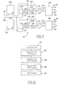
- the device comprises a time base 100, controlled by a processing unit 200.
- the time base 100 attacks on the one hand a measurement unit 300 receiving the capacitor Cx to test, on the other hand a unit 400 connected to the measurement unit 300, which is sensitive to the response of the capacitor to the periodic slot and which performs the sampling and an analog / digital conversion of the signal, the latter then being applied to the aforementioned processing unit 200, which then determines said parameters Coo, Rs, Ci and Ri.
- the processing unit 200 ensures, in addition to controlling the sequencing of the different bursts of slots generated by the time base 100 and the processing tasks proper, relations with conventional peripherals, such as printer 500, display screen or keyboard 600 and additional memory 700, and if necessary with an operating robot 800.
- the robot 800 can be used to ensure automatic insertion of the capacitors Cx into the measurement chain integrated into the unit 300, and an evacuation of said capacitors, with classification, based on an exploitation of the output information.
- the essential function of the time base 100 is to generate the excitation slots and the sampling pulses.
- the purpose of the time base 100 is to generate several ranges of periods of excitation slots accompanied by sampling pulses progressively offset from the successive times of application of the stimulus, as well as the introduction of fixed delays, to allow safe observation of the start of the response.
- the sampling times must constantly respect the minimum analog / digital conversion time.
- the processing unit applies sequencing signals on the time base 100.
- the processing unit 200 ensures the general reset of the device. To simplify the representation, the reset inputs of the components of the time base 100 have not been shown in FIG. 8.
- the processing unit 200 generates at its output 201 a signal for validation of the first range of excitation and sampling slots.
- a first series of data is acquired by sampling and conversion of the signal present at the output of the measurement unit 300.
- the processing unit 200 counts the number of acquired data.
- the output 201 is disabled and the processing unit generates on its output 202 a signal for validation of the second range of excitation slots and sampling pulses. A second series of data is then acquired.
- the output 202 is disabled and the processing unit generates on its output 203 a slot of 800 ms and a period sampling signal for example equal to 160 they.
- the different periods of the excitation slots and of the sampling pulses of the first and second bursts are determined by divisions of the frequency of a clock 101.
- the latter could be composed for example of an oscillator with logic gates controlled by a quartz of frequency 5 MHz.
- the first burst of excitation slots is obtained by dividing the clock frequency by 1000 which leads to slots of period 200 ⁇ s, while the sampling pulses are obtained by dividing the clock frequency by 1001 which leads to pulses with a period of 200.2 ⁇ s.
- the frequency of the clock 101 is divided by 500 thanks to three counters 102, 103, 104, connected in cascade, which ensure respectively a division by 10, 10 and 5 and which attack (counter 104) a monostable M105 which controls the counters 102, 103 and 104 by its output Q. More specifically, the monostable M105 controls by its output U the counting, in the absence of a reset signal on the counters 102, 103 and 104.
- the output Q of the monostable M105 controls by the rising edge a monostable M106 which has a pulse duration ⁇ , as shown on the second and third lines of the timing diagram of FIG. 9 the first line of which schematically represents the signal at the output of the clock 101.
- the Q output of the monostable M106 attacks a JK107 flip-flop which changes state with each falling edge of the signal at the Q output of the monostable M106, as shown in the fourth line of FIG. 9.
- the output of this JK107 flip-flop is connected to the first terminal 109 of an AND gate 108 which receives on its second terminal 110 the validation signal of the first burst (output 201 of the processing unit 200).
- the output of the AND gate 108 is connected to the first terminal 112 of an OR gate 111. It will be noted that the flip-flop JK107 ensures a division by two of the frequency of the signal at the output of the monostable M106.
- the output 113 of the OR gate 111, on which the excitation slots are available, is connected to the measurement unit 300.
- the delay introduced by the monostable M106 with respect to the origin of the times, is intended to compensate for the delay brought by the sampler-blocker integrated into the unit 400. This provision will be explained later.
- said delay p introduced by the monostable M106 is chosen to be greater than the minimum duration of the sampling pulse, so that one obtains some samples of zero value taken during the low level of the slot. stimulation corresponding to the reset phase.
- the signals present at the output of the flip-flop JK107 are found at the output 113 of the OR gate 111 when the AND gate 108 is validated, that is to say when a high level signal is applied to the input 110 of this by the output 201 of the processing unit.
- the sampling pulses are obtained by dividing the frequency of the clock 101 by 1001 to obtain pulses of period 200.2 they.
- This division by 1001 is operated by the element referenced 120 in FIG. 8.
- this element 120 may consist of four counters 121, 122, 123 and 124 capable of counting from N to 9 with 0 ⁇ N ⁇ 9 and prepositioned to 8999.
- the counting chain 121-122-123 and 124 attacks a monostable M125 which by its output Q controls the counting in the absence of a reset signal on the counters 121, 122, 123 and 124.
- the Q output of the monostable M125 will be validated when the count reaches 10,000, which from 8,999 to 10,000 leads to a division by 1001.
- the output Q, referenced 126 of the monostable 125, which constitutes the output of the element 120, is connected to the first terminal 129 of an AND gate 127, which receives on its second terminal 128 the validation signal of the first burst issued of the output 201 of the processing unit 200.
- the output 130 of the AND gate 127 is connected to the first terminal 132 of an OR gate 131 with three inputs, the output 135 of which is connected to the sampling and analog / digital conversion unit 400.
- the signals present at the output 126 of the monostable 125 are found at the output 135 of the OR gate 131 when the AND gate 127 is enabled, that is to say when a high level signal is applied to the input 128 of it by the output 201 of the processing unit.
- the second burst of excitation slots is obtained by dividing by 10 the frequency of the excitation slots of the first range, which leads to stimulation slots of periods of 2 ms, while the sampling pulses of the second burst are obtained by dividing the clock frequency by 1010, which leads to pulses of 202 ps periods.
- the output of the flip-flop JK107 is connected to the first terminal 141 of an AND gate 140 with two inputs, which receives on its second terminal 142 the validation signal of the second burst (output 202 of the processing unit 200).
- the output 143 of the AND gate 140 is connected to the input of a member 144 ensuring a division by 10 of the frequency of the signal present at the output of the flip-flop JK107.
- the output 145 of the member 144 is connected to the first terminal 147 of a gate 146 of the ET type, with two inputs, which receives on its second input terminal 148 the validation signal of the second burst (output 202 of the processing unit 200).
- the output 149 of the AND gate 146 is connected to the second input terminal 150 of the aforesaid OR gate 111.
- the signals present at the output of the divider member 144 are found at the output 113 of the OR gate 111 when the AND gate 146 is validated, that is to say when a high level signal is applied to the input 148 thereof by the output 202 of the processing unit 200.
- the sampling pulses accompanying this second burst are obtained by dividing the frequency of the clock 101 by 1010 to obtain pulses of period 202 ⁇ s.
- This division by 1010 is operated by the element referenced 160 in FIG. 8.
- this element 160 could consist, similar to the aforementioned element 120 of four counters 161, 162, 163 and 164 capable of counting from N to 9, with 0 ⁇ N ⁇ 9 and prepositioned at 8990.
- the counting chain 161-162-163 and 164 attacks a monostable M165 which, by its output Q controls the counting of the aforementioned counters 161, 162, 163 and 164 in the absence of reset signal thereon .
- the input of the first counter 161 of the element 160 is connected to the output 171 of an AND gate 170 with two inputs.
- the inputs 172 and 173 of this gate 170 are respectively connected to the output of the clock 101 and to the output 202 of the processing unit 200 validating the second range.
- the Q output of monostable 165 will be validated when the count of element 160 has reached 10,000, which from 8,990 to 10,000 leads to division by 1010.
- the output 175 of the AND gate 172 is connected to the second terminal 133 of the above-mentioned OR gate 131 with three inputs, the output 135 of which is connected to the unit sampling and analog / digital conversion 400.
- pulses with a period of 202 microseconds are obtained, slightly greater than a submultiple of the period of the stimulation slots and which therefore gradually shift relative to them. this.
- the signals present at the output 166 of the monostable M165 are found at the output 135 of the OR gate 131, when the AND gate 172 is validated, that is to say when a high level signal is applied to the input 173 of the latter by the output 202 of the processing unit 200.
- the third range is made up of a single slot whose duration is for example 800 ms, with real-time sampling of tight steps up to 32 ms and more loose steps for the rest of the time.
- the stimulation step of 800 ms duration is generated by the processing unit 200 on its output 203.
- the latter is connected to the third input terminal 151 of the OR gate 111.
- the real-time sampling is controlled directly by the processing unit 200, by its output 204 which is connected to the third terminal 134 of the OR gate 131.
- successive responses to the periodic stimulation slots can be considered as the superimposition of the beginnings of the response at the level and of stages whose value in the first slot evolves from one slot to another.
- the Applicant proposes to correct the amplitude value measured during the nth slot with the value of the amplitude measured at equivalent time during the first slot.
- the Applicant proposes to take a reference sample, for each stimulation slot, at a predetermined fixed instant thereof.
- the Q output of this M106 monostable has a falling edge synchronous with the original clock pulses.
- Said output Q of the monostable M106 is connected to the input 177 of a flip-flop JK176 which performs a division by 2 of the frequency of the signals coming from the monostable 106. Consequently the output of the flip-flop JK176 delivers slots of periods 200 ⁇ s not lagging behind the origin of time.
- the output 178 of the flip-flop JK176 is connected to the first input terminal 180 of an AND gate 179 with two inputs, which receives on its second input 181 the validation signal of the first range from the output 201 of the processing unit 200.
- the output 182 of the AND gate 179 is connected to the first input terminal 137 of an OR gate 136 with two inputs, the output 139 of which is connected to the sampling unit 400, in order to order the acquisition of reference samples, during the first range.
- the output 178 of the flip-flop JK176 is connected to a first input terminal 184 of an AND gate 183 with two inputs.
- the second terminal 185 of this AND gate 183 is connected to the output 202 of the processing unit 200 validating the second range.
- the output 186 of the AND gate 183 is connected to the input of a frequency-dividing member 187 by 10, the output of which 188 is connected to the first input terminal 190 of an AND gate 189 with two inputs, which receives on its second input terminal 191 the second range validation signal from output 202.
- the output 192 of the AND gate 189 with two inputs is connected to the second input terminal 138 of the OR gate 136.
- the dividing member 187 generates at the output slots of periods 2 ms.
- the signals present at the output of the flip-flop JK176 are found at the output 139 of the OR gate 136 when the AND gate 179 is validated, that is to say when a high level signal is applied to the input 181 of it by the output 201 of the processing unit.
- a signal with a period of 2 ms is present at the output of the dividing member 187 when the AND gate 183 is enabled, (when a high level signal is applied to the input 185 thereof by the output 202 of the processing unit, and therefore the AND gate 189 being validated in parallel), the signal present at the output of the member 187 is found at the output 139 of the OR gate 136.
- the counters 102, 103, 104, 121, 122, 123, 124, 161, 162, 163, and 164 are of the type 74 192
- the monostables M105, M106 and M125, M165 are of type 74 122
- flip-flops JK107, 176 are of type 7476.
- the measurement unit 300 illustrated diagrammatically in FIG. 7 and detailed in FIG. 10 has the function of operating a shaping of the excitation slots coming from the output 113 of the time base 100, from the amplitude point of view. , rise time and reference to zero of the low level, to detect the response of the sample to stimuli, through the measurement chain formed by the capacitive divider Cx and Cr, while achieving the isolation of the exit point of the chain measurement and the transfer of the response without disturbance, as well as by carrying out the reset to zero of the point of exit of the measurement chain during the idle times of the stimulus.
- the shaping of the stimulation slots is carried out by a shaping stage comprising an amplifier stage 302 and a transistor T ,. More specifically, the output 113 of the time base 100 is connected to the input 301 of the measurement unit 300, which is itself connected to the input 303 of the abovementioned amplifier operator 302.
- the output 304 of this operator is connected via a resistor R305 to the base of the transistor T, of the NPN type mounted as a common collector.
- the collector of transistor T is in fact connected to a positive supply terminal + VCC.
- the collector of transistor T is also connected to the output 304 of the operator 302 via a resistor R306.
- the emitter of transistor T is connected to the ground of the assembly via a resistor R307.
- the emitter of transistor T is also connected to a first terminal of capacitor Cx to be tested.
- the second terminal of this capacitor is connected to a first terminal of the capacitor Cr integrated in the measurement chain, which is connected by its second terminal to the ground of the assembly.
- the measurement chain is attacked by stimulation slots from the transistor emitter T ,.
- the reference capacitor Cr is chosen to be of the order of magnitude approximately 1000 times greater than the nominal value of the capacitor Cx to be tested.
- the measurement unit 300 advantageously includes means making it possible to modify the reference capacitor Cr by switching. These means have not been shown in FIG. 10 in order to simplify the illustration.
- the output of the measurement chain is taken between the common point between the capacitor Cx to be tested and the reference capacitor Cr.
- the voltage level at the output of this cell is low (around 15 mV).
- the measuring chain is shielded, as shown in 308, in FIG. 10, in order to avoid the superposition of noise on the useful signal.
- This device operates in parallel on the reference capacitor Cr. Of course, this device must at least disturb the behavior in pure capacitance of the reference capacitor. Nevertheless, the Applicant has demonstrated that over the whole range of useful frequencies, the reset device, during the active phase of the process, that is to say the high level of the stimulation window, can be likened to a scheme. equivalent combining in parallel a constant capacity and a constant resistance.
- Said capacity of the order of a few pF, is added to the capacity of the reference capacitor Cr and can easily be taken into account.
- the parasitic resistance due to the reset device is very high and does not, in practice, disturb the capacitive behavior of the reference capacitor.
- the input 301 of the measurement unit 300 is connected to the input 309 of an amplifier stage 310.
- the output 311 of this is connected via a resistor R312 to a negative supply terminal -V cc .
- the output 311 of the amplifier stage 310 is connected to the cathode of a Zener Z diode 313 .
- the anode of this diode Z 313 is connected via a resistor R314 to the ground of the assembly.
- the anode of this diode Z 313 is connected to the base of a bipolar PNP T2 transistor mounted as a common emitter.
- the emitter of this transistor T2 is in fact connected to the ground of the assembly, while its collector is connected to a negative supply terminal - V DC via a load resistor R315.
- collector of transistor T2 is connected to the gate of a field effect transistor T3, the source-drain channel of which is inserted, by means of a resistor R316 between the ground of the assembly and the point common to capacitors to be tested Cx and reference Cr.
- the transistor T2 is conductive and the field effect transistor T3 whose gate is brought to zero potential is conductive.
- the transistor T2 is blocked and brings the gate of the field effect transistor T3 to a strongly negative potential blocking the latter.
- the output of the Cx-Cr measuring chain is connected to a decoupling stage which aims to transmit the response while modifying the admittance of the reference capacity Cr as little as possible.
- This decoupling stage is formed by an operational amplifier OP317 with internal frequency correction.
- This operational amplifier OP317 is connected directly by one of its inputs to the point common to the capacitors to be tested Cx and of reference Cr, while its output is connected directly to its second input, to form a feedback loop.
- the OP317 amplifier is thus mounted as a voltage follower.
- such an operational amplifier OP317 can be of the LH 0052 type.
- the Applicant has found that such a device gave full satisfaction.
- the above circuit has an input resistance greater than 10 10 ohms.
- the input impedance due to the operational amplifier OP317 introduces an error on the tangent the angle of dielectric losses, as the order of 10 -4 at 10 Hz. in addition, this error decreases rapidly with increasing frequency.
- the above-mentioned decoupling stage is followed by at least one amplification stage.
- the decoupling stage OP317 is followed by two inverting amplifiers connected in cascade.
- the output of the amplifier OP317 is connected to the mass of the assembly by means of a resistor R318. Furthermore, the output of the amplifier OP317 is connected via a resistor R319 to the first input terminal of an amplifier OP320, the second input of which is connected to ground. The output of this operational amplifier OP320 is looped back to said first input thereof via a resistor R321. The output of the OP320 amplifier is connected via a resistor R322 to the first input of a second OP323 amplifier mounted as an inverter. To do this, the second input 324 of the amplifier OP323 is connected to ground while the output 325 of this same amplifier is looped back to the first input via a resistor R326.
- the output 325 of the operational amplifier OP323 is connected to the sampling unit 400.
- the operational amplifiers OP320 and OP323 are of the AD507 and AD509 type, while the amplifier stages 302 and 310 are of the 7416 type.
- the test device according to the present invention must allow the control of the usual capacitor values, and must therefore cover at least the range from 1 pF to ⁇ F. This range cannot be covered with a single reference capacitor. To do this, the Applicant proposes to divide the measurement process into two main ranges.
- the first main range concerns the testing of capacitors with a capacity between 0.3 pF and 30,000 pF.
- the second main range concerns the testing of capacitors with a capacity greater than 30,000 pF.
- the first main range is itself divided into five auxiliary sub-ranges.
- the first auxiliary sub-range concerns the capacitors to be tested with a capacity ranging from 0.3 to 3 pF.
- This first auxiliary sub-range uses a reference capacity of 1000 pF.
- the second auxiliary sub-range concerns the capacitors to be tested with a capacity ranging from 3 to 30 pF.
- This second auxiliary sub-range uses a reference capacity of 10,000 pF.
- the third auxiliary sub-range concerns the capacitors to be tested with a capacity ranging from 30 to 300 pF.
- This third auxiliary sub-range uses a reference capacity of 100,000 pF.
- the fourth auxiliary sub-range concerns the capacitors to be tested with a capacity ranging from 300 to 3000 pF.
- This fourth auxiliary sub-range uses a reference capacity of 1 pF.
- the fifth auxiliary sub-range concerns the capacitors to be tested with a capacity ranging from 3000 pF to 30,000 pF.
- This fifth auxiliary sub-range uses a reference capacity of 10 ⁇ F.
- the Applicant proposes, to avoid a loss of definition, to invert the reference capacitor Cr and the capacitor to be tested Cx, with respect to the mode shown in FIG. 10.
- the reference capacitor Cr on which the stimulation slots are applied must respect the Cr-Cx / 1000 relationship.
- the response detected by the decoupling stage (amplifier OP317) is then taken across the terminals of the capacitor to be tested Cx.
- the Applicant has demonstrated that the response thus taken responds to the relationship: It will indeed be noted that this expression (13), applicable for the second main measurement range, is very close to the relationships previously exposed. Therefore, the processing unit can use the same type of processing and the same algorithms as those which will be discussed later.
- the sampling and conversion unit 400 schematically represented in FIG. 7 and shown in more detail in FIG. 11 has the essential function of operating the sampling of the data, while ensuring the transfer interface between the unit 300 and the processing unit 200.
- sampling and conversion unit 400 is to transform sample values into a binary code (on 10 bits). born from the analog response from the measurement unit 300.
- the sampling and conversion unit 400 is connected to the measurement unit 300 via its input 402, to the time base 100 via its inputs 401 and 421, and finally, downstream, to the processing unit 200 via its outputs 451, 452 and 461, 462.
- the sampling unit 400 comprises in cascade, a blocking sampler 405, an adjustable gain amplifier 415 and an analog / digital converter 450.
- the device is suitable for taking, in addition to the measurement samples which pass through the blocking sampler chain 405 - amplifier 415 and converter 450, reference samples taken at a fixed instant from each stimulation slot.
- the sampling and conversion unit comprises, in parallel with the above-mentioned chain, a second chain through which the reference data pass and which also includes in cascade a blocking sampler 425 followed by an adjustable gain amplifier 435 and an analog / digital converter 460.
- the purpose of the blocking sampler 405 is to ensure, under the control of the time base 100 the acquisition and then the maintenance of the analog samples.
- the blocking sampler 405 shown diagrammatically in FIG. 11, essentially comprises an operational amplifier 406, a controllable switch 409 and an amplifier stage 411.
- a first input 407 of the operational amplifier 406 is connected to the input 402 of the sampling unit 400, to receive the analog signals coming from the measurement unit 300.
- the output 408 of the operational amplifier 406 is capable of being connected via the controllable switch 409 to the input 412 of the amplifier stage 411.
- the output of this amplifier stage 411 is connected to the second input 414 of the operational amplifier 406.
- the controllable switch 409 is controlled by the state of a signal applied to the input 410 of the blocking sampler 405.
- This input 410 is also connected to the output U of a monostable 420 whose input is connected to the input 401 of the unit 400.
- This input 401 is connected to the output 135 of the time base 100 for receiving the sampling pulses generated by it.
- the second blocking sampler 425 comprises an operational amplifier 426, a first input 427 of which is connected to the input 402 of the sampling unit to receive the analog signals coming from the measurement unit 300.
- the output 428 of the operational amplifier 426 can be connected via a controllable switch 429 to the input 432 of an amplifier stage 431 whose output is looped back to the second input 434 of the amplifier 426.
- L the controllable switch 429 is controlled by the state of the input 430 of the circuit 425.
- This input 430 is connected to the output Q of a monostable 440 whose input is connected to the input 421 of the unit 400.
- This input 421 is connected to the output 139 of the time base to receive the reference sampling pulses.
- the blocker samplers 405, 425 can be formed from the AD 582 type circuit sold by the company ANALOG DEVICES. Such a circuit can ensure the sampling of analog signals of 10 V peak to peak in a time of 6 seconds. Furthermore, the blocker samplers 405, 425 have a holding time for information on their respective output 413, 433 of the order of 25 they, entirely compatible with the conversion time of 25 they required by the converters 450, 460 , arranged downstream.
- sampling of the measurement data is carried out by the closing-opening process of the controllable switch 409 integrated into the blocking sampler 405, this closing-opening process being controlled by the sampling pulses from output 135 of time base 100.
- the reference sampling is established by the closing-opening process of the controllable switch 429 integrated into the sampler 425, this closing-opening process being controlled by the sampling pulses coming from the output 139 of the time base 100.
- each of the blocking samplers 405, 425 has a non-zero sampling gate closing time, as well as a time for tracking the output voltage relative to the non-zero input voltage.
- the stimulation slots present on the output 113 of the time base 100 are delayed with respect to the sampling pulses.
- the first samples likely to be retained are established on the low level of the stimulation slots and are therefore of zero value. Therefore, by retaining the first non-zero sample as the first valid sample, the delays specific to the sampling-blocking process do not disturb the measurement.
- the value at the origin of the response curve is determined not on the basis of the first acquired data, but by extrapolation on the basis of the second and the third. data.
- the outputs 413 and 433 of the sampler-blockers 405, 425 are respectively connected to the inputs of amplifiers with adjustable gain 415, 435.
- the latter make it possible to adapt the dynami that of output of the sampler-blocker 405, 425 respectively to the dynamic input of the analog / digital converter 450, 460.
- the respective outputs 416 and 436 of the amplifiers 415 and 435 are connected to the inputs of the converters 450 and 460.
- the latter can be formed, for example, of the AD 571 type circuit. Such circuits convert an sampled analog input signal into words 10 bits.
- the digital signals generated respectively by the converters 450 and 460 are available on the respective data buses 452 and 462 of these devices, which are connected to the processing unit 200.
- the converters 450 and 460 when the digital data are available on the aforementioned buses 452 and 462, the converters 450 and 460 generate on their outputs 451, 461, coded DR, a low level signal.
- the digital data remains present on the buses 452, 462, for processing by the processing unit 200, until the end of the control window applied on the converters 450 and 460 by the Q output of the monostables 420 and 440 respectively, as shown in Figure 11.
- the essential functions of this unit are to control the time base 100 by means of sequencing signals, for the generation of the different bursts of excitation slots and of sampling pulses and to ensure relations with conventional peripherals. 500, 600 and 700 and, where appropriate, a robot 800, as well as processing signals from the sampling unit 400 and analog / digital conversion.
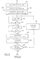
- the processing process successively comprises an initialization phase 210, a phase 220 of acquisition of the first range of data, a phase 240 of acquisition of the second range of data, a phase 260 of acquisition of the third range of data and finally a phase 270 of actual processing.
- the initialization phase 210 makes it possible to introduce the coefficients necessary for the completion of the processing phase 270, that is to say the coefficients necessary for the determination of the parameters (steps 272, 273, 274 and 275) and tolerance standards for classifying capacitors (step 276).
- the acquisition of data which aims to store these before the processing operation, is divided into three phases 220, 240 and 260 respectively, corresponding to the three ranges of excitation slots. and sampling pulses defined by the time base 100.
- the subroutines of the first and second acquisition phases 220, 240 take into account in addition to the measurement sample due to the sampling pulses generated at the output 135 of the time base 100, l ' reference sample due to the sampling pulses generated at the output 139 of the time base 100, to compensate for the effect of the stages induced by the reset, and which evolves from one slot to another.
- the process 220 begins with a step 221 of resetting to zero with time delay of the time base 100.
- Step 221 is followed by a step 222 of initializing the registers determining on the one hand the number of data previously stored and on the other hand the number of the address of the first data.
- Step 222 is followed by step 223 during which the processing unit validates the output 201, by applying a high level signal thereto, and invalidates the outputs 202, 203 and 204 by applying a signal. low level on these.
- the system is then ready for data acquisition.
- This acquisition is however conditioned by the DR line test of the analog / digital converter 450. Indeed, a high level signal on the DR line indicates that data is being converted, and transfer should only be authorized when the DR line goes low.
- This waiting process is determined by schematic steps 224 to 227.
- step 224 which follows step 223, the processing unit reads the state of the line DR and tests the state of the line DR in step 225.
- step 225 is followed by step 226 which will determine a waiting loop.
- step 224 is repeated after step 225.
- step 226 the processing unit 200 again reads the state of the line DR and this state is tested in the next step 227.
- step 226 of reading the state of the line DR is repeated.
- step 227 is followed by step 228 of correction.
- the aim of this correction procedure is to cancel the effect of the stages due to the resetting of the signal during low half-vibrations of the excitation slots.
- the correction on the measurement signal Y nm taken at the instant m of the n th excitation slot is carried out using the reference signals (due to the reference sampling signals generated on the output 139 of the time base 100 ).
- the correction uses, on the one hand, the reference sample Y ,, taken during the first excitation niche at time r and the reference sample Y nf taken in the n th niche at the equivalent time r.
- the correction stage 228 is followed by the storage step 229.
- This last step 229 is followed by a test step 230 during which the processing unit 200 searches if the number of stored data equals a predetermined number p.
- p 500 since 500 data of 0.2 ⁇ s must be taken.
- step 224 is repeated after incrementing the data storage address during intermediate step 231.
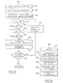
- step 230 If the test in step 230 is positive, the acquisition phase of the first range is completed and this step 230 is followed by the phase 240 of acquisition of the second range.
- the process 240 begins with a step 241 of resetting with time delay of the time base 100.
- Step 241 is followed by a step 242 of initializing the registers determining on the one hand the number of data memorized during the second acquisition phase, and on the other hand the number of the memory storage address. the first data of the second acquisition phase.
- Step 242 is followed by step 243 during which the processing unit 200 validates the output 202, by applying a high level signal thereto, and invalidates the outputs 201, 203 and 204, by applying a low level signal on them.
- the system is then ready for the second phase of data acquisition.
- step 244 which follows step 243, the processing unit 200 reads the state of the line DR, and tests the state of this line in step 245.
- step 245 If the line DR is at a high level, a piece of data being converted, step 245 is followed by step 246 which will determine a waiting loop.
- step 244 is repeated after step 245.
- step 246 the processing unit 200 again reads the state of the line DR and this state is tested in the next step 247.
- step 246 of reading the state of the line DR is repeated.
- step 247 is followed by step 248 of correction.
- This correction process is carried out on the measurement signal Y nm taken at the instant m from the n th excitation slot using the sample. of reference Y lr taken during the first excitation niche at time r and the reference sample Y nr taken in n th niche at the equivalent time r, on the basis of the relation.
- the correction step 248 is followed by the storage step 249.
- This storage step 249 is followed by a test step 250 during which the processing unit 200 searches if the number of stored data equals a predetermined number q.
- step 244 is repeated after defining a new storage address in intermediate step 251. This will be explained below.
- step 250 If on the other hand, the test in step 250 is positive, the second acquisition phase 240 is completed, and step 250 is followed by step 260 of acquisition of the third range.
- the data are not obtained in their natural order: 1st, 2nd ... but according to a sequence presenting an interlacing: 1st, 6th, 11th ... 2nd, 7th, 12th. due to the fact that 5 samples are taken for each stimulation slot.
- step 251 the processing unit must define the addresses for storing the data according to an interlaced sequence respecting the actual order of acquisition of the data.
- the processing unit 200 must take into account the reference samples as and when they are generated.
- the third acquisition phase 260 aims to study the behavior of the capacitor at low frequency.
- the processing unit 200 directly generates a single stimulation step as well as sampling pulses in real time.
- the third acquisition phase 260 can be operated on the basis of the following three sub-steps.
- the acquisition of 200 data is operated continuously with a sampling step of 160 ⁇ s up to 32 ms.
- the acquisition of 9 data is operated with a step of 8 ms up to 96 ms.
- this third acquisition phase has 223 points.
- the processing phase 270 begins with a step 271 of smoothing the raw data stored not in the order of acquisition but in the natural order of the samples.
- the aim of this smoothing step is to refine the data, affected by random disturbances mainly due to the quantization error and the error over the acquisition time.
- the smoothing is carried out by a mobile averaging method.
- the average value Ym of a sample assigned to time is defined. based on the relationship: However, the number of support points considered for establishing the moving average increases from the start of each range to the end of it to take into account the fact that the variations of the signal are faster at the start of the range than at the end of the range.
- the first 10 points are not smoothed, the following points are smoothed on three points and the end of the range uses a press on 8 points.
- the processing unit then proceeds to determine the parameters during steps 272, 273 and 274 which will be explained later.
- the Applicant has determined on this basis that the law of correspondence being linear, it is possible to acquire the characteristic parameters directly on the function y (t) in the form of intermediate parameters, during steps 272, 723 and 274, by subsequently transforming these into real parameters Coo, 1 / Rs, Ci, Ri and Cs in the consecutive step 275.
- step 272 the processing unit 200 determines the intermediate parameters ys and 1 / ps.
- the parameter 1 / ps is determined by the slope of the curve for long times.
- the parameter ys is determined by extending the slope at the origin.
- the slope of the curve is determined at several points, for example at times 32 ms, 96 ms and 720 ms and the relative values of the slope are compared.
- the capacitor has a conductance behavior of 1 / ps.
- the processing unit 200 determines that the capacitor exhibits a conductance behavior determined by the slope at instant 96 ms, from frequency 1 / 2 ⁇ 96 ms ⁇ 1.6 Hz.
- the parameter ys is then determined on the basis of a relation equivalent to relation (23).
- the three slopes are different, they indicate the presence of a relaxation phenomenon which evolves over time.
- step 273 the processing unit 200 determines the intermediate parameter ⁇ ⁇ .
- the parameter y corresponds to the first stored value.
- this point is marred by an error due to the uncertainty on the sampling time at the start of the response, on the one hand, and on the value of the first stored point, on the other hand.
- the parameter ⁇ ⁇ is determined by extrapolation from the second and third stored points.
- t 2 represents the sampling instant for the 2nd stored point
- 8T represents the sampling step.
- the time t'o of the true origin of the response is unknown. It can be equal to t 2 - ⁇ T in the case where an ideal sampling of the first point is made and equal to t 2 -2 ⁇ T in the other extreme case, which leads to locating on average the origin at time:
- the Applicant has determined that the error made in the determination of the parameter ⁇ ⁇ , by virtue of the aforementioned process, error which is due on the one hand to the uncertainty on the true origin time included in the interval t 2 - 2 ⁇ T ⁇ t'o ⁇ t 2 - 8T and on the other hand a certainty on the amplitude, is negligible.
- step 274 the processing unit 200 determines the intermediate parameters 1 / pi and yi.
- the intermediate parameter 1 / pi is, in theory, obtained by subtracting from the initial slope the term of conductivity 1 / ps, since the initial slope equals 1 / ⁇ s + 1 / ⁇ i.
- the relaxation time ⁇ j of each active branch of the FOSTER model is determined by detection of the abscissa of the maximums of the curve ⁇ '(logt).
- the processing unit 200 then detects the ordinates u (tj) and ⁇ (tj + 1) of the curve ⁇ (t) for the times tj and tj + 1. The difference between these ordinates ( ⁇ (tj + 1) - ⁇ (tj) gives directly the value 1 / T i and therefore the value ⁇ i.
- the processing unit 200 determines the real parameters, from the aforementioned intermediate parameters, on the basis of relations (17) to (22).
- the signal at the output of the measurement unit 300 responds to the relationship: relationship in which
- V represents the amplitude of the excitation slot
- G represents the gain of the system
- H represents a constant linked essentially to the reset device connected to the terminals of the reference capacitor.
- step 276 the processing unit 200 operates a classification of the capacitors.
- This classification is to detect the compliance or non-compliance of the capacitors with the standards provided for in a specification and consequently to monitor the quality of the manufacturing. To operate the classification or compare the real parameters Coo mes , Csmes and Rmes with ideal parameters Cooth, Csth and Rth stored in memory during the initialization step 210.
- a compliance signal is sent.
- step 210 a step of validity or tolerance in percentage ( ⁇ x%) of the nominal value Cn is memorized in step 210.
- the processing unit 200 emits a signal indicating the conformity of the capacitor with regard to the parameter Coo.
- the processing unit 200 proceeds in the same way for the parameters Cs and Ri.
- the results of the three classification procedures relating to the three parameters are stored in memory.
- the memorized signals can be used to control the robot 800 playing the role of sorting machine.
- Sorting may require, for example, that the three parameters comply with standards, or take into account the values of each of these three parameters separately.
- step 274 it is possible to avoid determining the slope ⁇ (t) for the evaluation of the parameters 1 / pi and Ci.
- the processing unit 200 may be formed for example of a microcomputer card of the ECB85 type sold by the company SIEMENS. It will be recalled that this card includes a microprocessor 8085, two parallel input / output doors 8185, an active static RAM memory with a capacity of 1 byte, a monitor program and a circuit type 8279 providing the interface with the keyboard 600.
Abstract
Description
La présente invention concerne un procédé et un dispositif pour le test rapide de condensateurs et de matériaux diélectriques.The present invention relates to a method and a device for the rapid testing of capacitors and dielectric materials.
Les dispositifs jusqu'ici proposés pour réaliser des tests sur des matériaux diélectriques ou des condensateurs soit n'opèrent qu'à une seule fréquence, soit s'avèrent particulièrement longs (voir par exemple FR-A-2 164 316).The devices hitherto proposed for carrying out tests on dielectric materials or capacitors either operate only at one frequency, or prove to be particularly long (see for example FR-A-2 164 316).
La présente invention vient maintenant proposer un nouveau procédé et dispositif permettant d'obtenir rapidement la réponse en fréquence desdits matériaux diélectriques ou condensateurs sur une large gamme de fréquences, par exemple de 10 Hz à 1 MHz.The present invention now proposes a new method and device making it possible to rapidly obtain the frequency response of said dielectric materials or capacitors over a wide range of frequencies, for example from 10 Hz to 1 MHz.
La présente invention permet ainsi un contrôle beaucoup plus complet.The present invention thus allows much more complete control.
Plus précisément, la présente invention a pour but de déterminer les paramètres Ri, Ci d'un condensateur, ou matériau diélectrique représenté par un modèle de FOSTER, tel qu'illustré sur la figure 1 annexée.More specifically, the purpose of the present invention is to determine the parameters Ri, Ci of a capacitor, or dielectric material represented by a FOSTER model, as illustrated in FIG. 1 appended.
On rappelle que le théorème de FOSTER montre qu'un condensateur imparfait peut être représenté par un réseau équivalent composé d'une association de capacités et de résistances. Comme représenté sur la figure 1 annexée, ce réseau équivalent comporte, en parallèle, un certain nombre (n) de branches formées chacune d'une résistance Ri et d'une capacité Ci, connectées en série, et en outre, deux branches particulières, également en parallèle, qui rendent compte des conditions limites, et qui comprennent l'une une capacité pure Coo, l'autre une résistance pure RS.It is recalled that the FOSTER theorem shows that an imperfect capacitor can be represented by an equivalent network composed of an association of capacitances and resistances. As shown in FIG. 1 appended, this equivalent network comprises, in parallel, a certain number (n) of branches each formed of a resistor Ri and of a capacitor Ci, connected in series, and in addition, two particular branches, also in parallel, which account for the boundary conditions, and which one includes a pure Coo capacity, the other a pure resistance R S.
Ceci conduit, à écrire la capacité du condensateur sous la forme:![]()
![]()
La présente invention a par conséquent pour but de déterminer les paramètres Coo, Rs, Ri et Ci précités.The present invention therefore aims to determine the parameters Coo, Rs, Ri and Ci above.
Le procédé de test de matériaux diélectriques, en particulier de condensateurs, conforme à la présente invention, comprend les étapes consistant:
- i) à insérer l'élément à tester en série d'une impédance de référence dans une chaîne de mesure,
- ii) à appliquer à la chaîne de mesure des créneaux répétitifs de stimulation,
- iii) à remettre à zéro la tension aux bornes de l'impédance de référencé, au cours de chaque demi-alternance inactive des créneaux de stimulation,
- iv) à échantillonner la réponse obtenue aux bornes de l'impédance de référence pour chaque créneau de stimulation, à des temps décalés progressivement par rapport aux créneaux de stimulation,
- v) à analyser les échantillons pour en déduire les paramètres de l'élément testé selon un modèle de FOSTER.
- i) inserting the element to be tested in series with a reference impedance in a measurement chain,
- ii) applying repetitive stimulation slots to the measurement chain,
- iii) resetting the voltage across the terminals of the referenced impedance, during each inactive half-wave of the stimulation slots,
- iv) sampling the response obtained at the limits of the reference impedance for each stimulation slot, at times progressively offset from the stimulation slots,
- v) to analyze the samples in order to deduce therefrom the parameters of the element tested according to a FOSTER model.
Plus précisément, selon l'invention, l'impédance de référence est un condensateur qui, de préférence, possède une capacité supérieure d'environ 1000 fois à celle de l'élément à tester.More specifically, according to the invention, the reference impedance is a capacitor which, preferably, has a capacity approximately 1000 times greater than that of the element to be tested.
Selon une caractéristique importante de l'invention, les étapes ii) et iv) d'application de créneaux répétitifs de stimulation et d'échantillonnage sont organisées en une pluralité de salves de créneaux dont les périodes croissent d'une salve à l'autre.According to an important characteristic of the invention, steps ii) and iv) of applying repetitive stimulation and sampling slots are organized into a plurality of slot bursts whose periods increase from one burst to another.
Les étapes ii) et iv) précitées comprennent avantageusement successivement:
- - l'application d'une première série de créneaux de stimulation de période constante, accompagnée d'une série d'impulsions d'échantillonnage de période constante et légèrement supérieure à celle des créneaux de stimulation,
- - l'application d'une seconde série de créneaux de stimulation de période constante et nettement supérieure à celle des créneaux de stimulation de la première série, accompagnée d'une seconde série d'impulsions d'échantillonnage de période constante et légèrement supérieure à un sous-multiple de celle des créneaux de stimulation,
- - l'application d'un créneau de stimulation unique de longue durée accompagnée d'impulsions d'échantillonnage de pas progressivement croissants.
- - the application of a first series of stimulation slots of constant period, accompanied by a series of sampling pulses of constant period and slightly greater than that of the stimulation slots,
- - the application of a second series of stimulation slots of constant period and clearly greater than that of the stimulation slots of the first series, accompanied by a second series of sampling pulses of constant period and slightly greater than one submultiple of that of the stimulation slots,
- - the application of a single long-term stimulation slot accompanied by sampling pulses of progressively increasing steps.
De façon avantageuse, la période des créneaux de stimulation de la première série est de l'ordre de 200 Its, la période des créneaux de stimulation de la seconde série est de l'ordre de 2 ms et le dernier créneau de stimulation présente une durée supérieure à 700 ms.Advantageously, the period of the stimulation slots of the first series is of the order of 200 I ts, the period of the stimulation slots of the second series is of the order of 2 ms and the last stimulation slot has a duration greater than 700 ms.
Selon une autre caractéristique avantageuse de l'invention, l'étape v) d'analyse comprendAccording to another advantageous characteristic of the invention, step v) of analysis comprises
va) la détermination de la pente finale de la réponse comme étant représentative du paramètre 1/RS du modèle de FOSTER etva) determining the final slope of the response as being representative of the
vb) la détermination de la valeur initiale asymptotique de la réponse comme étant représentative du paramètre Cs du modèle de FOSTER, Cs = C,oo + Ci.vb) the determination of the initial asymptotic value of the response as being representative of the parameter Cs of the FOSTER model, Cs = C, oo + Ci.
Plus précisément, de façon avantageuse, selon l'invention, l'étape va) consiste à comparer la pente de la réponse à différents instants et à retenir comme pente finale la valeur de pente reconnue identique pour plusieurs instants, et l'étape vb) consiste à déterminer la valeur initiale asymptotique en soustrayant de la valeur du nème échantillon le produit de la pente finale et de l'abscisse du nème échantillon.More precisely, advantageously, according to the invention, step va) consists in comparing the slope of the response at different times and to retain as the final slope the value of slope recognized identical for several times, and step vb) consists in determining the initial asymptotic value by subtracting from the value of the n th sample the product of the final slope and the abscissa of the n th sample.
Selon une autre caractéristique avantageuse de l'invention, l'étape v) comprendAccording to another advantageous characteristic of the invention, step v) comprises
vc) la détermination de la valeur initiale de la réponse comme étant représentative du paramètre Cx du modèle de FOSTER.vc) determining the initial value of the response as being representative of the parameter Cx of the FOSTER model.
Plus précisément, de façon avantageuse, selon l'invention, l'étape vc) consiste à déterminer la valeur initiale de la réponse par extrapolation à partir des deuxième et troisième échantillons en considérant l'origine moyenne to des temps comme étant égale à:![]()
![]()
t2 représente l'instant d'acquisition du second échantillon ett 2 represents the acquisition time of the second sample and
8T représente le pas d'échantillonnage.8T represents the sampling step.
Selon une autre caractéristique avantageuse de l'invention, l'étape v) comprendAccording to another advantageous characteristic of the invention, step v) comprises
vd) la détermination de l'amplitude des paliers de la courbe de la pente de la réponse comme étant représentative du paramètre 1/Ri du modèle de FOSTER etvd) the determination of the amplitude of the steps of the curve of the slope of the response as being representative of the
ve) la détermination des abscisses des maximum de la dérivée de la pente de la réponse comme étant représentative du temps de relaxation des différentes branches R-C du modèle de FOSTER.ve) the determination of the abscissae of the maximums of the derivative of the slope of the response as being representative of the relaxation time of the different R-C branches of the FOSTER model.
Selon une autre caractéristique avantageuse de l'invention, l'étape v) d'analyse comprend l'étape de conversion des paramètres y(t) déterminés sur la base des échantillons pour obtenir les paramètres de la capacité, selon la loi d'étalonnage linéaire:
- C(t) = K [y(t) + a], dans lesquels K et a sont des constantes.
- C (t) = K [y (t) + a], where K and a are constants.
De façon préférentielle, selon l'invention, le procédé de test comprend l'étape préliminaire consistant
- - à disposer deux condensateurs étalons Cr1 et Cr2 en série dans la chaîne de mesure,
- - à détecter la réponse v'(t) à un échelon de stimulation d'amplitude V appliqué à la chaîne de mesure, telle que

- G représente le gain du système, et
- a' représente une constante additive due à la remise à zéro de la chaîne de mesure, et la phase v) de traitement comprend en outre l'étape consistant
- - à corriger les valeurs mesurées y(t) sur la base des coefficients G et a pour obtenir les paramètres de la capacité C(t) selon le modèle de FOSTER répondant à la relation:

- - to have two standard capacitors Cr 1 and Cr 2 in series in the measurement chain,
- - detecting the response v '(t) at a stimulation step of amplitude V applied to the measurement chain, such as
- G represents the gain of the system, and
- a 'represents an additive constant due to the reset of the measurement chain, and the processing phase v) further comprises the step consisting
- - to correct the measured values y (t) on the basis of the coefficients G and a to obtain the parameters of the capacity C (t) according to the FOSTER model corresponding to the relation:
De préférence, le procédé de test comprend en outre l'étape ultérieure de classement des éléments testés sur la base des paramètres déterminés à l'aide des échantillons.Preferably, the test method further comprises the subsequent step of classifying the elements tested on the basis of the parameters determined using the samples.
De façon avantageuse, le procédé de test comprend en outre les étapes consistant à prélever un échantillon de référence Ynr pour chaque créneau à un instant r constant de ces créneaux et à corriger avant l'étape v) d'analyse chaque échantillon Ynm sur la base de la relation![]()
![]()
Ynr représente l'échantillon de référence pris au néme créneau et
- Ylr représente l'échantillon de référence pris lors du premier créneau.
- Y lr represents the reference sample taken during the first slot.
Le dispositif de test de matériau diélectrique, en particulier de condensateur, conforme à la présente invention comprend:
- - une unité de mesure apte à recevoir l'élément à tester en série d'une impédance de référence dans une chaîne de mesure,
- - une base de temps apte à appliquer à la chaîne de mesure des créneaux répétitifs de stimulation
- - des moyens adaptés pour remettre à zéro la tension aux bornes de l'impédance de référence au cours de chaque demi-alternance inactive des créneaux de stimulation,
- - une unité d'échantillonnage sensible à la réponse obtenue aux bornes de l'impédance de référence pour chaque créneau de stimulation, et qui échantillonne cette réponse à des temps décalés progressivement par rapport aux créneaux de stimulation,
- - une unité de traitement qui analyse les échantillons établis par l'unité d'échantillonnage pour en déduire les paramètres de l'élément testé, selon un modèle de FOSTER.
- a measurement unit capable of receiving the element to be tested in series with a reference impedance in a measurement chain,
- - a time base capable of applying repetitive stimulation slots to the measurement chain
- means adapted to reset the voltage across the reference impedance to zero during each inactive half-cycle of the stimulation slots,
- a sampling unit sensitive to the response obtained at the terminals of the reference impedance for each stimulation slot, and which samples this response at times progressively offset from the stimulation slots,
- - a processing unit which analyzes the samples established by the sampling unit in order to deduce therefrom the parameters of the element tested, according to a FOSTER model.
De préférence, l'impédance de référence est un condensateur de référence qui possède une capacité supérieure d'environ 1000 fois à celle de l'élément à tester.Preferably, the reference impedance is a reference capacitor which has a capacity approximately 1000 times greater than that of the element to be tested.
Selon une caractéristique avantageuse de l'invention, l'unité de mesure possède des moyens permettant de modifier l'impédance de référence insérée dans la chaîne de mesure.According to an advantageous characteristic of the invention, the measurement unit has means making it possible to modify the reference impedance inserted in the measurement chain.
Selon une autre caractéristique avantageuse de l'invention, l'unité d'échantillonnage comprend un convertisseur analogique/numérique.According to another advantageous characteristic of the invention, the sampling unit comprises an analog / digital converter.
De préférence, l'unité de traitement contrôle la base de temps de telle sorte que celle-ci génère plusieurs salves successives de créneaux de stimulation dont les périodes croissent d'une salve à l'autre.Preferably, the processing unit controls the time base so that it generates several successive bursts of stimulation slots whose periods increase from one burst to another.
Plus précisément, de façon préférentielle, la base de temps génère successivement
- - une première série de créneaux de stimulation de période constante, accompagnée d'une série d'impulsions d'échantillonnage de période constante et légèrement supérieure à celle des créneaux de stimulation,
- - une seconde série de créneaux de stimulation de période constante et nettement supérieure à celle des créneaux de stimulation de la première série, accompagnée d'une seconde série d'impulsions d'échantillonnage de période constante et légèrement supérieure à un sous-multiple de celle des créneaux de stimulation, puis
- - un créneau de stimulation unique de longue durée accompagnée d'impulsions d'échantillonnage de pas progressivement croissants.
- - a first series of stimulation slots of constant period, accompanied by a series of sampling pulses of constant period and slightly greater than that of the stimulation slots,
- - a second series of stimulation slots of constant period and clearly greater than that of the stimulation slots of the first series, accompanied by a second series of sampling pulses of constant period and slightly greater than a submultiple of that stimulation slots, then
- - a unique long-term stimulation window accompanied by sampling pulses of progressively increasing steps.
Plus précisément encore, de façon avantageuse, la période des créneaux de stimulation de la première série est de l'ordre de 200 ps, la période des créneaux de stimulation de la seconde série est de l'ordre de 2 ms et le dernier créneau de stimulation présente une durée supérieure à 700 ms.More precisely still, advantageously, the period of the stimulation slots of the first series is of the order of 200 ps, the period of the stimulation slots of the second series is of the order of 2 ms and the last slot of stimulation lasts more than 700 ms.
Selon une autre caractéristique avantageuse de la présente invention, la base de temps comprend:
- - une horloge,
- - plusieurs diviseurs de fréquence attaqués par l'horloge et déterminant des créneaux de stimulation de périodes respectives,
- - des portes de type ET connectées en sortie des diviseurs et validées alternativement par l'unité de traitement,
- - une porte de type OU dont les entrées sont reliées respectivement en sortie des portes de type ET, et à la sortie de laquelle sont disponibles les créneaux de stimulation.
- - a clock,
- - several frequency dividers attacked by the clock and determining stimulation slots of respective periods,
- - ET type doors connected to the output of the dividers and validated alternately by the processing unit,
- - an OR type door, the inputs of which are connected respectively at the output of the AND type doors, and at the output of which the stimulation slots are available.
Selon une autre caractéristique avantageuse de l'invention, la base de temps comprend:
- - une seconde série de diviseurs de fréquence attaqués par l'horloge et déterminant des impulsions d'échantillonnage de périodes respectives,
- - une seconde série de portes de type ET connectées respectivement en sortie des diviseurs de fréquence de la seconde série et qui sont validées alternativement par l'unité de traitement en synchronisme avec l'une associée des portes ET de la première série, et
- - une seconde porte de type OU dont les entrées sont reliées respectivement en sortie des portes ET de la deuxième série et à la sortie de laquelle sont disponibles les impulsions d'échantillonnage.
- - a second series of frequency dividers attacked by the clock and determining sampling pulses of respective periods,
- a second series of AND type doors connected respectively at the output of the frequency dividers of the second series and which are validated alternately by the processing unit in synchronism with one associated with the AND doors of the first series, and
- - a second OR-type gate, the inputs of which are connected respectively to the output of the AND gates of the second series and to the output of which the sampling pulses are available.
Selon l'invention, de préférence, la base de temps génère par ailleurs des impulsions d'échantillonnage auxiliaires, à un instant constant de chaque créneau de stimulation, pour le prélèvement d'échantillons de référence.According to the invention, preferably, the time base also generates auxiliary sampling pulses, at a constant instant of each stimulation slot, for the taking of reference samples.
Selon une autre caractéristique préférentielle de l'invention, l'unité de mesure comprend entre la chaîne de mesure et l'unité d'échantillonnage, successivement, un étage de découplage à impédance d'entrée très élevée et au moins un étage d'amplification.According to another preferred characteristic of the invention, the measurement unit comprises, between the measurement chain and the sampling unit, successively, a decoupling stage with very high input impedance and at least one amplification stage .
De préférence, de plus, la liaison entre la chaîne de mesure et l'étage de découplage est blindée.Preferably, moreover, the connection between the measuring chain and the decoupling stage is shielded.
Selon une autre caractéristique de l'invention, les moyens de remise à zéro de la tension aux bornes de l'impédance de référence possèdent une impédance de sortie très élevée.According to another characteristic of the invention, the means for resetting the voltage across the terminals of the reference impedance have a very high output impedance.
Selon un mode de réalisation avantageux, les moyens de remise à zéro comprennent un transistor à effet de champ.According to an advantageous embodiment, the reset means comprise a field effect transistor.
Selon une autre caractéristique avantageuse de l'invention, l'unité d'échantillonnage comprend en cascade un échantillonneur bloqueur, un étage amplificateur et un convertisseur analogique/ numérique.According to another advantageous characteristic of the invention, the sampling unit comprises in cascade a blocking sampler, an amplifier stage and an analog / digital converter.
D'autres caractéristiques et avantages de la présente invention apparaîtront à la lecture de la description détaillée qui va suivre, donnée à titre d'exemples non limitatifs, et en regard des dessins annexés, sur lesquels, la figure 1 qui représente un modèle de FOSTER, ayant déjà été décrite:
- - la figure 2 représente schématiquement la chaîne de mesure utilisée dans un dispositif conforme à la présente invention,
- - la figure 3 représente la courbe de réponse à un échelon de stimulation,
- - la figure 4 représente la pente de la courbe de réponse,
- - la figure 5 représente la dérivée de la pente de la courbe de réponse,
- - la figure 6a illustre schématiquement un cycle de test comprenant différentes salves de créneaux de stimulation et d'impulsions d'échantillonnage,
- - la figure 6b illustre schématiquement les créneaux de stimulation, la réponse et les impulsions d'échantillonnage de la première salve,
- - la figure 6c illustre les créneaux de stimulation, la réponse et les impulsions d'échantillonnage de la deuxième salve,
- - la figure 7 représente schématiquement la structure générale du dispositif de test conforme à la présente invention,
- - la figure 8 représente la structure de la base de temps intégrée au dispositif de test conforme à la présente invention,
- - la figure 9 illustre la forme des signaux considérés en différents points de la base de temps du dispositif de la présente invention,
- - la figure 10 représente la structure de l'unité de mesure intégrée au dispositif conforme à la présente invention,
- - la figure 11 représente la structure de l'unité d'échantillonnage - conversion analogique/ numérique intégrée au dispositif de test conforme à la présente invention,
- - la figure 12 illustre schématiquement le processus de traitement des échantillons,
- - la figure 13 illustre le processus d'acquisition de la première gamme d'échantillons,
- - la figure 14 illustre schématiquement le processus d'acquisition de la seconde gamme d'échantillons,
- - la figure 15 illustre le processus de traitement proprement dit des échantillons.
- FIG. 2 schematically represents the measurement chain used in a device according to the present invention,
- FIG. 3 represents the response curve at a stimulation level,
- FIG. 4 represents the slope of the response curve,
- FIG. 5 represents the derivative of the slope of the response curve,
- FIG. 6a schematically illustrates a test cycle comprising different bursts of stimulation slots and sampling pulses,
- FIG. 6b schematically illustrates the stimulation slots, the response and the sampling pulses of the first burst,
- FIG. 6c illustrates the stimulation slots, the response and the sampling pulses of the second burst,
- FIG. 7 schematically represents the general structure of the test device according to the present invention,
- FIG. 8 represents the structure of the time base integrated into the test device according to the present invention,
- FIG. 9 illustrates the shape of the signals considered at different points of the time base of the device of the present invention,
- FIG. 10 represents the structure of the measurement unit integrated into the device according to the present invention,
- FIG. 11 represents the structure of the sampling unit - analog / digital conversion integrated into the test device according to the present invention,
- FIG. 12 schematically illustrates the process for processing the samples,
- FIG. 13 illustrates the process of acquiring the first range of samples,
- FIG. 14 schematically illustrates the process of acquiring the second range of samples,
- - Figure 15 illustrates the actual processing process of the samples.
La description détaillée qui va suivre concernera le test d'un condensateur. Cette description, ainsi que les dessins s'y rapportant ne doivent en aucune façon être considérés comme limitatifs. En effet, l'invention, d'une façon générale, s'applique aux tests de matériaux diélectriques.The detailed description which follows will relate to the testing of a capacitor. This description, as well as the drawings relating thereto, must in no way be considered as limiting. Indeed, the invention, in general, applies to the testing of dielectric materials.
On va décrire successivement, par la suite, 1. le principe de la mesure, 2. la structure générale du dispositif, 3. la structure de la base de temps, 4. la structure de l'unité de mesure, 5. la structure de l'unité d'échantillonnage-conversion analogique/ numérique et 6. la fonction et la structure de l'unité de traitement.We will describe successively, below, 1. the principle of measurement, 2. the general structure of the device, 3. the structure of the time base, 4. the structure of the measurement unit, 5. the structure of the analog / digital sampling-conversion unit and 6. the function and structure of the processing unit.
Comme cela est illustré sur la figure 2, le principe à la base de l'invention consiste à appliquer un échelon de tension V à une chaîne de mesure comportant le condensateur Cx à mesurer connecté en série avec un condensateur de référence Cr, ce dernier étant choisi de telle sorte que Cx < < Cr.As illustrated in FIG. 2, the principle underlying the invention consists in applying a voltage step V to a measurement chain comprising the capacitor Cx to be measured connected in series with a reference capacitor Cr, the latter being chosen so that Cx <<Cr.
On démontre alors que, en utilisant la notation de Laplace:


Dans le cas d'un domaine de dispersion unique, c'est-à-dire le cas où n = 1, les paramètres du circuit équivalent peuvent être obtenus très facilement.In the case of a single dispersion domain, that is to say the case where n = 1, the parameters of the equivalent circuit can be obtained very easily.
En effet, comme cela est représenté sur la figure 3, les valeurs Coo et Cs,Indeed, as shown in FIG. 3, the values Coo and Cs,
![]()
![]()
Le terme de conductivité 1/Rs est déterminé par analyse de la pente a de l'asymptote, tga = 1/Rs. La conductance 1/R, est déterminé par analyse de la pente y à l'origine, en effet tgy = 1/Rs + 1/R1, tandis que le temps de relaxation τ = R1C1 est déterminé par l'intersection de la pente initiale et de l'asymptote à la courbe.The
Dans le cas de plusieurs domaines (n>1), l'analyse de la pente, représentée sur la figure 4,In the case of several domains (n> 1), the analysis of the slope, represented in FIG. 4,

Ces valeurs 1/Ri sont en effet égales aux largeurs des paliers de la courbe de pente λ(t), comme représenté sur la figure 4.These
L'analyse de cette courbe permet également d'accéder aux termes RiCi = Ti qui correspondent pour chaque palier à l'abscisse de l'ordonnée 0,37/Ri.Analysis of this curve also gives access to the terms RiCi = T i which correspond for each plateau to the abscissa of the ordinate 0.37 / Ri.
Par ailleurs, l'analyse de la dérivée seconde λ'(t) représentée sur la figure 5 permet de connaître le nombre de domaines de relaxation (correspondant au nombre de maximum) ainsi que les valeurs Ti précitées (correspondant aux abscisses desdits maximum).Furthermore, the analysis of the second derivative λ '(t) represented in FIG. 5 makes it possible to know the number of relaxation domains (corresponding to the number of maximums) as well as the abovementioned values T i (corresponding to the abscissas of said maximums) .
Pour couvrir un domaine fréquentiel de test allant de 10 Hz à 1 MHz, en tenant compte du théorème d'échantillonnage de SHANNON d'une part et de l'influence des fréquences supérieures à la borne limite arbitraire supérieure considérée Fm = 10 MHz, on prend une période d'échantillonnage To≃ 1/2πFM, soit To = 0,2 µs.To cover a frequency test range from 10 Hz to 1 MHz, taking into account the Shannon sampling theorem on the one hand and the influence of the frequencies above the upper limit arbitrary terminal considered F m = 10 MHz, we take a sampling period T o ≃ 1 / 2πF M , that is To = 0.2 µs.
Cependant, les composants classiques réalisant une conversion analogique/numérique sur 10 bits exigent un temps de conversion de l'ordre de 25 µs et exigeraient par conséquent, en théorie, une période d'échantillonnage au moins égale à 25 ps, incompatible avec la période 0,2 µs, ci-dessus déterminée.However, conventional components carrying out analog / digital conversion on 10 bits require a conversion time of the order of 25 µs and would therefore require, in theory, a sampling period at least equal to 25 ps, incompatible with the period 0.2 µs, above determined.
Pour contourner cette difficulté, selon une caractéristique importante de la présente invention, la Demanderesse propose de remplacer l'échelon de stimulation par un créneau périodique, en ramenant à zéro les conditions initiales du condensateur sous test avant chaque front montant du créneau, de façon à obtenir une répétition périodique du début de la réponse à l'échelon.To circumvent this difficulty, according to an important characteristic of the present invention, the Applicant proposes to replace the stimulation step by a periodic slot, by reducing to zero the initial conditions of the capacitor under test before each rising edge of the slot, so as to obtain a periodic repetition of the start of the step response.
Plus précisément, selon l'invention, on applique sur la chaîne de mesure un créneau périodique de période T et de rapport cyclique 1/2 et l'on échantillonne la réponse avec une période T+8T, supérieure à la période du créneau d'excitation, avec 8T = 0,2 µs. La remise à zéro du condensateur sous test est effectuée lors du niveau bas du signal rectangulaire d'excitation de rapport cyclique 1/2.More precisely, according to the invention, a periodic slot of period T and a
L'écart δT entre la période d'échantillonnage et la période de stimulation décale la position relative de l'échantillon n + i pris dans le créneau n + i par rapport à celle de l'échantillon n dans le créneau n.The difference δT between the sampling period and the stimulation period shifts the relative position of the sample n + i taken in the slot n + i with respect to that of the sample n in the slot n.
Ainsi, on réalise une transposition de temps et on dispose pour chaque échantillon équivalent à une durée 8T = 0,2 µs d'un temps T important, qui peut être largement supérieur à 25 ps, pour la conversion analogique numérique.Thus, a time transposition is carried out and there is for each sample equivalent to a duration 8T = 0.2 μs of a significant time T, which can be much greater than 25 ps, for the analog-to-digital conversion.
La remise à zéro du condensateur sous test Cx est réalisée en court-circuitant à la masse le condensateur de référence Cr connecté en série de ce dernier, de telle sorte que les deux extrémités du condensateur sous test soient au potentiel zéro.The capacitor under test Cx is reset to zero by short-circuiting the reference capacitor Cr connected in series to the latter, so that the two ends of the capacitor under test are at zero potential.
La Demanderesse a remarqué cependant que la différence de potentiel aux bornes des capacités Ci intégrées à une branche série Ci-Ri du modèle de FOSTER ne pouvait être annulée pendant la demi-alternance de niveau bas du créneau de stimulation que lorsque la constante de temps Ti = Ri Ci est petite devant le temps 0 de remise à zéro.The Applicant has noted, however, that the potential difference at the terminals of the capacitors Ci integrated into a series branch Ci-Ri of the FOSTER model could only be canceled during the half-cycle of the low level of the stimulation window only when the time constant T i = Ri Ci is small compared to
Dans le cas contraire, le signal obtenu est perturbé.Otherwise, the signal obtained is disturbed.
Dans le cas où le temps 0 de remise à zéro égale la demi-période d'échantillonnage T/2:
- - quand τi ≃ T/2, la réponse obtenue restitue la réponse à l'échelon avec un coefficient 1/1 +e-T/2t près,
- - quand Ti > > T/2, aucune composante n'est introduite par la branche correspondante dans le signal global.
- - when τi ≃ T / 2, the response obtained restores the response to the step with a
coefficient 1/1 + e -T / 2t , - - when T i>> T / 2, no component is introduced by the corresponding branch in the global signal.
Cependant, dans la pratique, pour des raisons technologiques, il convient d'éviter la simultanéité de l'application du stimulus et de la disparition de la remise à zéro. En d'autres termes, le temps de remise à zéro 0 du condensateur sous test Cx sera inférieur, dans la pratique, à la demi-période T/2 du créneau de stimulation.However, in practice, for technological reasons, the simultaneous application of the stimulus and the disappearance of the reset must be avoided. In other words, the
Cela altère également la réponse obtenue, et il en résulte que, en appelant AT l'écart entre le temps de remise à zéro et la demi-période de stimulation: 0 = T/2-ΔT:
- - pour τ> > T/2, la réponse donnée par le même créneau peut être exprimée par la relation

- - pour τ≃T/2, le régime permanent est atteint en 1 ou 2 périodes et la réponse donnée par le nème créneau peut être exprimée par la relation:

- - for τ>> T / 2, the answer given by the same time slot can be expressed by the relation
- - for τ≃T / 2, the steady state is reached in 1 or 2 periods and the response given by the n th slot can be expressed by the relation:
En comparant les relations précitées à la réponse à l'échelon:![]()
![]()
- avec un temps de remise à zéro 0 égal à la demi-période de stimulation, la réponse répétitive à chaque créneau est identique au début de la réponse à l'échelon, jusqu'à la fin de la durée du créneau, à un facteur près égal à![]()
![]()
- avec un temps de remise à zéro 0 inférieur à la demi-période de stimulation, les conclusions précédentes restent valables, si l'on annule ou compense le palier, constant pendant un créneau, et, en régime transitoire, variable d'un créneau à l'autre, qui résulte de l'existence de ΔT. Ce palier égale![]()
![]()
La première gamme peut être formée par exemple d'une salve de 500 créneaux de stimulus de période de 200 µs avec des signaux d'échantillonnage de la réponse d'une période de 200,2 µs constituant un vernier temporel par rapport à la stimulation. Cette gamme d'une durée réelle de 100 ms permet d'analyser des temps d'échantillonnage de 0,2 µs à 100 µs avec une période de 0,2 µs, couvrant ainsi l'équivalent d'une réponse fréquentielle de 1 MHz.The first range can be formed for example of a burst of 500 slots of stimuli of period of 200 μs with signals for sampling the response of a period of 200.2 μs constituting a temporal vernier with respect to the stimulation. This range with an actual duration of 100 ms makes it possible to analyze sampling times from 0.2 µs to 100 µs with a period of 0.2 µs, thus covering the equivalent of a frequency response of 1 MHz.
Un seul échantillon est prélevé par période de stimulation comme illustré sur la figure 6b et on dispose des 200 µs de cette période pour opérer l'échantillonnage et la conversion numérique.A single sample is taken per stimulation period as illustrated in FIG. 6b and the 200 μs of this period are available for sampling and digital conversion.
La deuxième gamme peut être formée par exemple de 10 créneaux de stimulation de période de 2 ms avec des impulsions d'échantillonnage de période 202 us. Cette gamme d'une durée réelle de 20 ms permet d'analyser des temps d'échantillonnage allant jusqu'à 1 ms avec un pas d'échantillonnage équivalent de 20 µs.The second range can be formed, for example, of 10 stimulation pits of period of 2 ms with sampling pulses of
Dans ce cas, 10 échantillons sont déterminés par période de stimulation dont cinq seulement sont utiles et correspondent à la demi-alternance de niveau haut de l'impulsion de stimulation. Là encore, on dispose d'un temps de conversion de l'ordre de 200 µs. Cette disposition est illustrée sur la figure 6c.In this case, 10 samples are determined per stimulation period of which only five are useful and correspond to the half-cycle of the high level of the stimulation pulse. Again, there is a conversion time of around 200 µs. This arrangement is illustrated in Figure 6c.
Enfin, la troisième gamme est composée d'un créneau unique dont la durée est par exemple de 800 ms avec un échantillonnage en temps réel de pas serré jusqu'à 32 ms, et de pas plus lâches pour le reste du temps.Finally, the third range is made up of a single slot whose duration is for example 800 ms with real-time sampling of tight steps up to 32 ms, and of no more loose for the rest of the time.
Les algorithmes permettant de déterminer les paramètres du condensateur Coo, Rs, Ri, Ci, seront précisés ultérieurement.The algorithms for determining the parameters of the capacitor Coo, Rs, Ri, Ci, will be specified later.
On va maintenant décrire la structure du dispositif représenté sur les figures 7 à 15.We will now describe the structure of the device shown in FIGS. 7 to 15.
Comme cela est représenté sur la figure 7, le dispositif conforme à la présente invention comprend une base de temps 100, contrôlée par une unité de traitement 200. La base de temps 100 attaque d'une part une unité de mesure 300 recevant le condensateur Cx à tester, d'autre part une unité 400 reliée à l'unité de mesure 300, qui est sensible à la réponse du condensateur au créneau périodique et qui réalise l'échantillonnage et une conversion analogique/numérique du signal, ce dernier étant ensuite appliqué à l'unité de traitement précitée 200, qui détermine alors lesdits paramètres Coo, Rs, Ci et Ri.As shown in FIG. 7, the device according to the present invention comprises a
La fonction et la structure de chacun de ces quatre blocs fonctionnels élémentaires 100, 200, 300 et 400 seront décrits plus en détail par la suite.The function and structure of each of these four elementary
On remarquera cependant dès à présent que l'unité de traitement 200 assure, outre le contrôle du séquencement des différentes salves de créneaux générés par la base de temps 100 et les tâches de traitement proprement dite, des relations avec des périphériques conventionnels, tels que imprimante 500, écran de visualisation ou clavier 600 et mémoire annexe 700, et le cas échéant avec un robot d'exploitation 800.However, it will now be noted that the
Les relations avec les périphériques conventionnels 500, 600, 700, assure la sortie des informations et l'entrée des consignes d'exploitation.Relations with
Le robot 800 peut être utilisé pour assurer l'insertion automatique des condensateurs Cx dans la chaîne de mesure intégrée à l'unité 300, et une évacuation desdits condensateurs, avec classement, sur la base d'une exploitation des informations de sortie.The
La base de temps 100 a pour fonction essentielle de générer les créneaux d'excitation et les impulsions d'échantillonnage.The essential function of the
Plus précisément, la base de temps 100 a pour but de générer plusieurs gammes de périodes de créneaux d'excitation accompagnés d'impulsions d'échantillonnage progressivement décalées par rapport au temps successifs d'application du stimulus ainsi que l'introduction de retards fixes, pour permettre l'observation sûre du début de la réponse. Les temps d'échantillonnage doivent respecter constamment le temps minimal de conversion analogique/digital.More specifically, the purpose of the
Comme cela est représenté schématiquement sur la figure 8, l'unité de traitement applique des signaux de séquencement sur la base de temps 100.As shown schematically in FIG. 8, the processing unit applies sequencing signals on the
Lors de la mise sous tension et au début de chaque cycle de mesure, l'unité de traitement 200 assure la remise à zéro générale du dispositif. Pour simplifier la représentation les entrées de remise à zéro des composants de la base de temps 100 n'ont pas été représentées sur la figure 8.During power-up and at the start of each measurement cycle, the
Dans un premier temps, l'unité de traitement 200 génère sur sa sortie 201 un signal de validation de la première gamme de créneaux d'excitation et d'échantillonnage. Une première série de données est acquise par échantillonnage et conversion du signal présent à la sortie de l'unité de mesure 300. L'unité de traitement 200 compte le nombre de données acquises.Firstly, the
Lorsque un nombre prédéterminé de données est obtenu, la sortie 201 est invalidée et l'unité de traitement génère sur sa sortie 202 un signal de validation de la seconde gamme de créneaux d'excitation et d'impulsions d'échantillonnage. Une seconde série de données est alors acquise.When a predetermined number of data is obtained, the
Là encore, lorsqu'un nombre prédéterminé de données est obtenu au cours de cette seconde acquisition, la sortie 202 est invalidée et l'unité de traitement génère sur sa sortie 203 un créneau de 800 ms et un signal d'échantillonnage de période par exemple égale à 160 ils.Again, when a predetermined number of data is obtained during this second acquisition, the
Les différentes périodes des créneaux d'excitation et des impulsions d'échantillonnage des première et seconde salves sont déterminées par divisions de la fréquence d'une horloge 101.The different periods of the excitation slots and of the sampling pulses of the first and second bursts are determined by divisions of the frequency of a
Cette dernière pourra être composée par exemple d'un oscillateur à portes logiques pilotées par un quartz de fréquence 5 MHz.The latter could be composed for example of an oscillator with logic gates controlled by a quartz of frequency 5 MHz.
La première salve de créneaux d'excitation est obtenue en divisant la fréquence de l'horloge par 1000 ce qui conduit à des créneaux de période 200 µs, tandis que les impulsions d'échantillonnage sont obtenues en divisant la fréquence de l'horloge par 1001 ce qui conduit à des impulsions de période de 200,2 µs.The first burst of excitation slots is obtained by dividing the clock frequency by 1000 which leads to slots of
Comme représenté sur la figure 8, la fréquence de l'horloge 101 est divisée par 500 grâce à trois compteurs 102, 103, 104, connectés en cascade, qui assurent respectivement une division par 10, 10 et 5 et qui attaquent (compteur 104) un monostable M105 qui contrôle les compteurs 102, 103 et 104 par sa sortie Q. Plus précisément, le monostable M105 commande par sa sortie U le comptage, en absence d'un signal de remise à zéro sur les compteurs 102, 103 et 104.As shown in FIG. 8, the frequency of the
La sortie Q du monostable M105 commande par le front montant un monostable M106 qui possède une durée d'impulsion β, comme représenté sur les deuxième et troisième lignes du chronogramme de la figure 9 dont la première ligne représente schématiquement le signal en sortie de l'horloge 101.The output Q of the monostable M105 controls by the rising edge a monostable M106 which has a pulse duration β, as shown on the second and third lines of the timing diagram of FIG. 9 the first line of which schematically represents the signal at the output of the
La sortie Q du monostable M106 attaque une bascule JK107 qui change d'état à chaque front descendant du signal à la sortie Q du monostable M106, comme représenté sur la quatrième ligne de la figure 9. La sortie de cette bascule JK107 est reliée à la première borne 109 d'une porte ET 108 qui reçoit sur sa seconde borne 110 le signal de validation de la première salve (sortie 201 de l'unité de traitement 200). La sortie de la porte ET 108 est reliée à la première borne 112 d'une porte OU 111. On remarquera que la bascule JK107 assure une division par deux de la fréquence du signal en sortie du monostable M106.The Q output of the monostable M106 attacks a JK107 flip-flop which changes state with each falling edge of the signal at the Q output of the monostable M106, as shown in the fourth line of FIG. 9. The output of this JK107 flip-flop is connected to the
La sortie 113 de la porte OU 111, sur laquelle sont disponibles les créneaux d'excitation est reliée à l'unité de mesure 300.The
Le retard introduit par le monostable M106 par rapport à l'origine des temps, a pour but de compenser le retard apporté par l'échantillonneur- bloqueur intégré à l'unité 400. Cette disposition sera explicitée par la suite.The delay introduced by the monostable M106 with respect to the origin of the times, is intended to compensate for the delay brought by the sampler-blocker integrated into the
Cependant, selon l'invention, ledit retard p introduit par le monostable M106 est choisi supérieur à la durée minimale de l'impulsion d'échantillonnage, de telle sorte que l'on obtienne quelques échantillons de valeur nulle pris pendant le niveau bas du créneau de stimulation correspondant à la phase de remise à zéro. Cette disposition permet de répérer clairement le premier échantillon réel qui est en fait le premier échantillon non nul.However, according to the invention, said delay p introduced by the monostable M106 is chosen to be greater than the minimum duration of the sampling pulse, so that one obtains some samples of zero value taken during the low level of the slot. stimulation corresponding to the reset phase. This arrangement makes it possible to clearly identify the first real sample which is in fact the first non-zero sample.
Comme cela ressort de la description qui précède et de l'examen des figures 8 et 9, on obtient ainsi à la sortie de la bascule JK107 (4ème ligne de la figure 9) des créneaux de période 200 µs et de rapport cyclique 1/2. Ces créneaux sont retardés d'une durée par rapport à l'origine des temps.As appears from the above description and from the examination of FIGS. 8 and 9, one thus obtains at the output of the flip-flop JK107 (4th line of FIG. 9) slots of
Les signaux présents à la sortie de la bascule JK107 se retrouvent à la sortie 113 de la porte OU 111 lorsque la porte ET 108 est validée, c'est-à-dire lorsque un signal de niveau haut est appliqué sur l'entrée 110 de celle-ci par la sortie 201 de l'unité de traitement.The signals present at the output of the flip-flop JK107 are found at the
Comme cela a été précédemment évoqué, les impulsions d'échantillonnage sont obtenues en divisant la fréquence de l'horloge 101 par 1001 pour obtenir des impulsions de période 200,2 ils.As previously mentioned, the sampling pulses are obtained by dividing the frequency of the
Cette division par 1001 est opérée par l'élément référencé 120 sur la figure 8.This division by 1001 is operated by the element referenced 120 in FIG. 8.
Dans la pratique, cet élément 120 pourra être constitué de quatre compteurs 121, 122, 123 et 124 capables d'effectuer un comptage de N à 9 avec 0 < N < 9 et prépositionnés à 8999. La chaîne de comptage 121-122-123 et 124 attaque un monostable M125 qui par sa sortie Q commande le comptage en absence d'un signal de remise à zéro sur les compteurs 121, 122, 123 et 124.In practice, this
La sortie Q du monostable M125 sera validée lorsque le comptage aura atteint 10 000, ce qui de 8999 à 10 000 conduit bien à une division par 1001.The Q output of the monostable M125 will be validated when the count reaches 10,000, which from 8,999 to 10,000 leads to a division by 1001.
La sortie Q, référencée 126 du monostable 125, qui constitue la sortie de l'élément 120, est reliée à la première borne 129 d'une porte ET 127, qui reçoit sur sa seconde borne 128 le signal de validation de la première salve issue de la sortie 201 de l'unité de traitement 200.The output Q, referenced 126 of the monostable 125, which constitutes the output of the
La sortie 130 de la porte ET 127 est reliée à la première borne 132 d'une porte OU 131 à trois entrées dont la sortie 135 est reliée à l'unité d'échantillonnage et de conversion analogique/ numérique 400.The
Comme cela ressort de la description qui précède, on obtient à la sortie 126 du monostable 125 des impulsions de période 200,2 ils qui se décalent donc progressivement par rapport aux créneaux de stimulation.As emerges from the above description, at the
Les signaux présents à la sortie 126 du monostable 125 se retrouvent à la sortie 135 de la porte OU 131 lorsque la porte ET 127 est validée, c'est-à-dire lorsqu'un signal de niveau haut est appliqué sur l'entrée 128 de celle-ci par la sortie 201 de l'unité de traitement.The signals present at the
La seconde salve de créneaux d'excitation est obtenue en divisant par 10 la fréquence des créneaux d'excitation de la première gamme, ce qui conduit à des créneaux de stimulation de périodes de 2 ms, tandis que les impulsions d'échantillonnage de la seconde salve sont obtenues en divisant la fréquence de l'horloge par 1010, ce qui conduit à des impulsions de périodes 202 ps.The second burst of excitation slots is obtained by dividing by 10 the frequency of the excitation slots of the first range, which leads to stimulation slots of periods of 2 ms, while the sampling pulses of the second burst are obtained by dividing the clock frequency by 1010, which leads to pulses of 202 ps periods.
On rappelle que au cours de cette seconde salve, on prélève non plus un échantillon mais cinq échantillons utiles par période de créneaux d'excitation, avec un pas équivalent de 20 µs.It will be recalled that during this second burst, no longer a sample is taken but five useful samples per period of excitation slots, with an equivalent step of 20 μs.
Comme cela est représenté sur la figure 8, la sortie de la bascule JK107 est reliée à la première borne 141 d'une porte ET 140 à deux entrées, qui reçoit sur sa seconde borne 142 le signal de validation de la seconde salve (sortie 202 de l'unité de traitement 200). La sortie 143 de la porte ET 140 est reliée à l'entrée d'un organe 144 assurant une division par 10 de la fréquence du signal présent à la sortie de la bascule JK107.As shown in FIG. 8, the output of the flip-flop JK107 is connected to the
La sortie 145 de l'organe 144 est reliée à la première borne 147 d'une porte 146 du type ET, à deux entrées, qui reçoit sur sa seconde borne d'entrée 148 le signal de validation de la seconde salve (sortie 202 de l'unité de traitement 200). La sortie 149 de la porte ET 146 est reliée à la seconde borne d'entrée 150 de la porte OU 111 précitée.The
Comme cela ressort de la description qui précède et de l'examen de la figure 8, on obtient ainsi à la sortie de l'organe 144 des créneaux de périodes de 2 ms et de rapport cyclique 1/2. Ces créneaux sont retardés d'une durée ε par rapport à l'origine des temps. Ce retard est introduit par le monostable 106 précité intercalé entre l'horloge 101 et l'organe diviseur 144.As is apparent from the above description and from the examination of FIG. 8, one thus obtains at the output of the
Les signaux présents à la sortie de l'organe diviseur 144 se retrouvent à la sortie 113 de la porte OU 111 lorsque la porte ET 146 est validée, c'est-à-dire lorsque un signal de niveau haut est appliqué sur l'entrée 148 de celle-ci par la sortie 202 de l'unité de traitement 200.The signals present at the output of the
Comme cela a été précédemment évoqué, les impulsions d'échantillonnage accompagnant cette seconde salve sont obtenues en divisant la fréquence de l'horloge 101 par 1010 pour obtenir des impulsions de période 202 µs.As previously mentioned, the sampling pulses accompanying this second burst are obtained by dividing the frequency of the
Cette division par 1010 est opérée par l'élément référencé 160 sur la figure 8.This division by 1010 is operated by the element referenced 160 in FIG. 8.
Dans la pratique, cet élément 160 pourra être constitué, de façon similaire à l'élément 120 précité de quatre compteurs 161, 162, 163 et 164 capables d'effectuer un comptage de N à 9, avec 0<N<9 et prépositionnés à 8990. La chaîne de comptage 161-162-163 et 164 attaque un monostable M165 qui, par sa sortie Q commande le comptage des compteurs précités 161, 162, 163 et 164 en l'absence de signal de remise à zéro sur ceux-ci.In practice, this
Par ailleurs, l'entrée du premier compteur 161 de l'élément 160 est relié à la sortie 171 d'une porte ET 170 à deux entrées. Les entrées 172 et 173 de cette porte 170 sont reliées respectivement à la sortie de l'horloge 101 et à la sortie 202 de l'unité de traitement 200 validant la seconde gamme.Furthermore, the input of the
La sortie Q du monostable 165 sera validée lorsque le comptage de l'élément 160 aura atteint 10 000, ce qui de 8990 à 10 000 conduit bien à une division par 1010.The Q output of monostable 165 will be validated when the count of
La sortie Q, référencée 166 du monostable M165, qui constitue la sortie de l'élément diviseur 160, est reliée à la première borne 174 d'une porte ET 172 à deux entrées qui reçoit sur sa seconde borne 173 le signal de validation de la seconde salve issue de la sortie 202 de l'unité de traitement 200. La sortie 175 de la porte ET 172 est reliée à la seconde borne 133 de la porte OU 131 précitée à trois entrées, dont la sortie 135 est reliée à l'unité d'échantillonnage et conversion analogique/ numérique 400.The output Q, referenced 166 of the monostable M165, which constitutes the output of the
Comme cela ressort de la description qui précède, on obtient à la sortie 166 du monostable M165 des impulsions de période 202 microsecondes, légèrement supérieure à un sous-multiple de la période des créneaux de stimulation et qui se décalent donc progressivement par rapport à ceux-ci.As is apparent from the above description, at the
Les signaux présents à la sortie 166 du monostable M165 se retrouvent à la sortie 135 de la porte OU 131, lorsque la porte ET 172 est validée, c'est-à-dire lorsque un signal de niveau haut est appliqué sur l'entrée 173 de celle-ci par la sortie 202 de l'unité de traitement 200.The signals present at the
Comme cela a été précédemment évoqué, la troisième gamme est composée d'un créneau unique dont la durée est par exemple de 800 ms, avec un échantillonnage en temps réel de pas serrés jusqu'à 32 ms et de pas plus lâches pour le reste du temps.As previously mentioned, the third range is made up of a single slot whose duration is for example 800 ms, with real-time sampling of tight steps up to 32 ms and more loose steps for the rest of the time.
L'échelon de stimulation d'une durée de 800 ms est généré par l'unité de traitement 200 sur sa sortie 203. Cette dernière est reliée à la troisième borne d'entrée 151 de la porte OU 111.The stimulation step of 800 ms duration is generated by the
Par ailleurs, l'échantillonnage en temps réel est commandé directement par l'unité de traitement 200, par sa sortie 204 qui est reliée à la troisième borne 134 de la porte OU 131.Furthermore, the real-time sampling is controlled directly by the
On a expliqué précédemment que les réponses successives aux créneaux de stimulation périodique peuvent être considérées comme la superposition des débuts de la réponse à l'échelon et de paliers dont la valeur au premier créneau évolue d'un créneau à l'autre.It has been explained previously that the successive responses to the periodic stimulation slots can be considered as the superimposition of the beginnings of the response at the level and of stages whose value in the first slot evolves from one slot to another.
Pour s'affranchir de cette perturbation, la Demanderesse propose de corriger la valeur d'amplitude mesurée lors du nème créneau grâce à la valeur de l'amplitude mesurée au temps équivalent lors du premier créneau.To overcome this disturbance, the Applicant proposes to correct the amplitude value measured during the nth slot with the value of the amplitude measured at equivalent time during the first slot.
Pour cela, en d'autres termes, la Demanderesse propose de prélever un échantillon de référence, pour chaque créneau de stimulation, à un instant fixe prédéterminé de ceux-ci.For this, in other words, the Applicant proposes to take a reference sample, for each stimulation slot, at a predetermined fixed instant thereof.
Pour cela, on utilise le signal présent sur la sortie Q du monostable M106. Comme cela est représenté sur la cinquième ligne de la figure 9, la sortie Q de ce monostable M106 possède un front descendant synchrone des impulsions d'horloge d'origine. Ladite sortie Q du monostable M106 est reliée à l'entrée 177 d'une bascule JK176 qui réalise une division par 2 de la fréquence des signaux issus du monostable 106. Par conséquent la sortie de la bascule JK176 délivre des créneaux de périodes 200 µs non retardés par rapport à l'origine des temps.For this, we use the signal present on the Q output of the monostable M106. As shown in the fifth line in Figure 9, the Q output of this M106 monostable has a falling edge synchronous with the original clock pulses. Said output Q of the monostable M106 is connected to the
Ces créneaux appliqués à l'unité d'échantillonnage 400 seront utilisés pour commander une acquisition auxiliaire d'échantillons de référence, sur chaque réponse à un créneau individuel à un temps fixe des périodes de ceux-ci. Pour ce faire, la sortie 178 de la bascule JK176 est reliée à la première borne d'entrée 180 d'une porte ET 179 à deux entrées, qui reçoit sur sa seconde entrée 181 le signal de validation de la première gamme issue de la sortie 201 de l'unité de traitement 200. La sortie 182 de la porte ET 179 est reliée à la première borne d'entrée 137 d'une porte OU 136 à deux entrées, dont la sortie 139 est reliée à l'unité d'échantillonnage 400, afin de commander l'acquisition d'échantillons de référence, lors de la première gamme.These slots applied to the
Bien entendu, il est nécessaire de procéder de même à l'acquisition d'échantillons de référence lors de la seconde gamme.Of course, it is necessary to do the same for the acquisition of reference samples during the second range.
Pour ce faire, on divise également la fréquence des créneaux non retardés de la première gamme issue de la bascule JK176, par 10.To do this, we also divide the frequency of the non-delayed slots of the first range from the flip-flop JK176, by 10.
Plus précisément, la sortie 178 de la bascule JK176 est reliée à une première borne d'entrée 184 d'une porte ET 183 à deux entrées. La seconde borne 185 de cette porte ET 183 est reliée à la sortie 202 de l'unité de traitement 200 validant la seconde gamme.More precisely, the
La sortie 186 de la porte ET 183 est reliée à l'entrée d'un organe 187 diviseur de fréquences par 10, dont la sortie 188 est reliée à la première borne d'entrée 190 d'une porte ET 189 à deux entrées, qui reçoit sur sa seconde borne d'entrée 191 le signal de validation de seconde gamme issu de la sortie 202.The
La sortie 192 de la porte ET 189 à deux entrées est reliée à la seconde borne d'entrée 138 de la porte OU 136.The
En conséquence, lors de la validation de la sortie 202 de l'unité de traitement 200, l'organe diviseur 187 génère en sortie des créneaux de périodes 2 ms.Consequently, during the validation of the
Les signaux présents à la sortie de la bascule JK176 se retrouvent à la sortie 139 de la porte OU 136 lorsque la porte ET 179 est validée, c'est-à-dire lorsqu'un signal de niveau haut est appliqué sur l'entrée 181 de celle-ci par la sortie 201 de l'unité de traitement.The signals present at the output of the flip-flop JK176 are found at the
Par contre, un signal de période 2 ms est présent à la sortie de l'organe diviseur 187 lorsque la porte ET 183 est validée, (lorsqu'un signal de niveau haut est appliqué sur l'entrée 185 de celle-ci par la sortie 202 de l'unité de traitement, et de ce fait, la porte ET 189 étant en parallèle validée), le signal présent en sortie de l'organe 187 se retrouve à la sortie 139 de la porte OU 136.On the other hand, a signal with a period of 2 ms is present at the output of the dividing
Selon un mode de réalisation donné à titre d'exemple non limitatif, les compteurs 102, 103, 104, 121, 122, 123, 124, 161, 162, 163, et 164 sont du type 74 192, les monostables M105, M106 et M125, M165 sont du type 74 122, tandis que les bascules JK107, 176 sont du type 7476.According to an embodiment given by way of nonlimiting example, the
L'unité de mesure 300 illustrée schématiquement sur la figure 7 et détaillée sur la figure 10 a pour fonction d'opérer une mise en forme des créneaux d'excitation provenant de la sortie 113 de la base de temps 100, au point de vue amplitude, temps de montée et référence à zéro du niveau bas, de détecter la réponse de l'échantillon aux stimulus, à travers la chaîne de mesure formée du diviseur capacitif Cx et Cr, tout en réalisant l'isolement du point de sortie de la chaîne de mesure et le transfert de la réponse sans perturbation, ainsi qu'en réalisant la remise à zéro du point de sortie de la chaîne de mesure pendant les temps morts du stimulus.The
La mise en forme des créneaux de stimulation est réalisée par un étage de mise en forme comprenant un étage amplificateur 302 et un transistor T,. Plus précisément, la sortie 113 de la base de temps 100 est reliée à l'entrée 301 de l'unité de mesure 300, qui est reliée elle-même à l'entrée 303 de l'opérateur amplificateur 302 précité.The shaping of the stimulation slots is carried out by a shaping stage comprising an
La sortie 304 de cet opérateur est reliée par l'intermédiaire d'une résistance R305 à la base du transistor T, du type NPN monté en collecteur commun.The
Comme cela est représenté sur la figure 10, le collecteur du transistor T, est en effet relié à une borne d'alimentation positive +VCC. Le collecteur du transistor T, est par ailleurs relié à la sortie 304 de l'opérateur 302 par l'intermédiaire d'une résistance R306.As shown in FIG. 10, the collector of transistor T, is in fact connected to a positive supply terminal + VCC. The collector of transistor T, is also connected to the
L'émetteur du transistor T, est relié à la masse du montage par l'intermédiaire d'une résistance R307.The emitter of transistor T, is connected to the ground of the assembly via a resistor R307.
L'émetteur du transistor T, est également relié à une première borne du condensateur Cx à tester. La seconde borne de ce condensateur est reliée à une première borne du condensateur Cr intégré à la chaîne de mesure, qui est relié par sa seconde borne à la masse du montage.The emitter of transistor T, is also connected to a first terminal of capacitor Cx to be tested. The second terminal of this capacitor is connected to a first terminal of the capacitor Cr integrated in the measurement chain, which is connected by its second terminal to the ground of the assembly.
Il en résulte que la chaîne de mesure est attaquée par des créneaux de stimulation issus de l'émetteur de transistor T,.As a result, the measurement chain is attacked by stimulation slots from the transistor emitter T ,.
Comme cela a été précédemment évoqué, le condensateur de référence Cr est choisi d'un ordre de grandeur d'environ 1000 fois supérieur à la valeur nominale du condensateur Cx à tester. Afin de respecter cette condition, l'unité de mesure 300 comporte avantageusement des moyens permettant de modifier par commutation le condensateur de référence Cr. Ces moyens n'ont pas été représentés sur la figure 10 afin de simplifier l'illustration.As previously mentioned, the reference capacitor Cr is chosen to be of the order of magnitude approximately 1000 times greater than the nominal value of the capacitor Cx to be tested. In order to comply with this condition, the
La sortie de la chaîne de mesure est prise entre le point commun entre le condensateur Cx à tester et le condensateur Cr de référence. Le niveau de la tension à la sortie de cette cellule est faible (de l'ordre de 15 mV). De ce fait, la chaîne de mesure est blindée, comme cela est représenté en 308, sur la figure 10, afin d'éviter la superposition de bruit sur le signal utile.The output of the measurement chain is taken between the common point between the capacitor Cx to be tested and the reference capacitor Cr. The voltage level at the output of this cell is low (around 15 mV). As a result, the measuring chain is shielded, as shown in 308, in FIG. 10, in order to avoid the superposition of noise on the useful signal.
On va maintenant décrire le dispositif permettant une remise à zéro du point de sortie de la chaîne de mesure pendant les temps morts des créneaux de stimulation.We will now describe the device for resetting the output point of the measurement chain to zero during the idle times of the stimulation slots.
Ce dispositif intervient en parallèle sur le condensateur de référence Cr. Bien entendu, ce dispositif doit perturber au minimum le comportement en capacitance pure du condensateur de référence. Néanmoins, la Demanderesse a démontré que sur toute la gamme de fréquences utiles, le dispositif de remise à zéro, pendant la phase active du processus, c'est-à-dire le niveau haut du créneau de stimulation, pouvait être assimilé à un schéma équivalent associant en parallèle une capacité constante et une résistance constante.This device operates in parallel on the reference capacitor Cr. Of course, this device must at least disturb the behavior in pure capacitance of the reference capacitor. Nevertheless, the Applicant has demonstrated that over the whole range of useful frequencies, the reset device, during the active phase of the process, that is to say the high level of the stimulation window, can be likened to a scheme. equivalent combining in parallel a constant capacity and a constant resistance.
Ladite capacité, de l'ordre de quelques pF s'ajoute à la capacité du condensateur de référence Cr et peut aisément être prise en compte. La résistance parasite due au dispositif de remise à zéro est très élevée et ne perturbe pas, en pratique, le comportement capacitif du condensateur de référence.Said capacity, of the order of a few pF, is added to the capacity of the reference capacitor Cr and can easily be taken into account. The parasitic resistance due to the reset device is very high and does not, in practice, disturb the capacitive behavior of the reference capacitor.
L'entrée 301 de l'unité de mesure 300 est reliée à l'entrée 309 d'un étage amplificateur 310. La sortie 311 de celui-ci est reliée par l'intermédiaire d'une résistance R312 à une borne d'alimentation négative -Vcc. Par ailleurs, la sortie 311 de l'étage amplificateur 310 est reliée à la cathode d'une diode Zener Z313. L'anode de cette diode Z313 est reliée par l'intermédiaire d'une résistance R314 à la masse du montage. Par ailleurs, l'anode de cette diode Z313 est reliée à la base d'un transistor bipolaire PNP T2 monté en émetteur commun.The
L'émetteur de ce transistor T2 est en effet relié à la masse du montage, tandis que son collecteur est relié à une borne d'alimentation négative - Vcc par l'intermédiaire d'une résistance de charge R315.The emitter of this transistor T2 is in fact connected to the ground of the assembly, while its collector is connected to a negative supply terminal - V DC via a load resistor R315.
De plus, le collecteur du transistor T2 est relié à la grille d'un transistor à effet de champs T3 dont le canal source-drain est inséré, par l'intermédiaire d'une résistance R316 entre la masse du montage et le point commun aux condensateurs à tester Cx et de référence Cr.In addition, the collector of transistor T2 is connected to the gate of a field effect transistor T3, the source-drain channel of which is inserted, by means of a resistor R316 between the ground of the assembly and the point common to capacitors to be tested Cx and reference Cr.
Pendant la demi-alternance de niveau bas des créneaux d'excitation, le transistor T2 est conducteur et le transistor à effet de champ T3 dont la grille est portée au potentiel zéro est conducteur.During the low-level half-wave of the excitation slots, the transistor T2 is conductive and the field effect transistor T3 whose gate is brought to zero potential is conductive.
A l'opposé, pendant les demi-alternances de niveau haut des créneaux d'excitation, le transistor T2 est bloqué et porte la grille du transistor à effet de champ T3 à un potentiel fortement négatif bloquant ce dernier.Conversely, during the half-wave high level of the excitation slots, the transistor T2 is blocked and brings the gate of the field effect transistor T3 to a strongly negative potential blocking the latter.
La sortie de la chaîne de mesure Cx-Cr est reliée à un étage de découplage qui a pour but de transmettre la réponse en modifiant le moins possible l'admittance de la capacité de référence Cr.The output of the Cx-Cr measuring chain is connected to a decoupling stage which aims to transmit the response while modifying the admittance of the reference capacity Cr as little as possible.
Cet étage de découplage est formé d'un amplificateur opérationnel OP317 à correction interne de fréquences. Cet amplificateur opérationnel OP317 est relié directement par l'une de ses entrées au point commun aux condensateurs à tester Cx et de référence Cr, tandis que sa sortie est reliée directement à sa seconde entrée, pour former une boucle de contre-réaction.This decoupling stage is formed by an operational amplifier OP317 with internal frequency correction. This operational amplifier OP317 is connected directly by one of its inputs to the point common to the capacitors to be tested Cx and of reference Cr, while its output is connected directly to its second input, to form a feedback loop.
L'amplificateur OP317 est ainsi monté en suiveur de tension. A titre d'exemple non limitatif, un tel amplificateur opérationnel OP317 peut être du type LH 0052. La Demanderesse a constaté qu'un tel dispositif donnait pleinement satisfaction. Le circuit précité présente une résistance d'entrée supérieure â 1010 ohms. Par ailleurs, même dans des conditions critiques pour lesquelles le condensateur de référence possède une valeur faible de l'ordre de 10-8 F, l'impédance d'entrée due à l'amplificateur opérationnel OP317 n'introduit une erreur sur la tangente de l'angle de pertes du diélectrique, que de l'ordre de 10-4 à 10 Hz. Par ailleurs, cette erreur diminue très vite quand la fréquence augmente.The OP317 amplifier is thus mounted as a voltage follower. By way of nonlimiting example, such an operational amplifier OP317 can be of the LH 0052 type. The Applicant has found that such a device gave full satisfaction. The above circuit has an input resistance greater than 10 10 ohms. Moreover, even in critical conditions in which the reference capacitor has a low value of the order of 10- 8 M, the input impedance due to the operational amplifier OP317 introduces an error on the tangent the angle of dielectric losses, as the order of 10 -4 at 10 Hz. in addition, this error decreases rapidly with increasing frequency.
L'étage de découplage précité est suivi d'au moins un étage d'amplification.The above-mentioned decoupling stage is followed by at least one amplification stage.
Plus précisément, selon le mode de réalisation représenté sur la figure 10, l'étage de découplage OP317 est suivi de deux amplificateurs inverseurs montés en cascade.More specifically, according to the embodiment shown in Figure 10, the decoupling stage OP317 is followed by two inverting amplifiers connected in cascade.
Plus précisément encore, la sortie de l'amplificateur OP317 est reliée à la'masse du montage par l'intermédiaire d'une résistance R318. Par ailleurs, la sortie de l'amplificateur OP317 est reliée par l'intermédiaire d'une résistance R319 à la première borne d'entrée d'un amplificateur OP320 dont la seconde entrée est reliée à la masse. La sortie de cet amplificateur opérationnel OP320 est rebouclée sur ladite première entrée de celui-ci par l'intermédiaire d'une résistance R321. La sortie de l'amplificateur OP320 est reliée par l'intermédiaire d'une résistance R322 à la première entrée d'un deuxième amplificateur OP323 monté en inverseur. Pour ce faire, la seconde entrée 324 de l'amplificateur OP323 est reliée à la masse tandis que la sortie 325 de ce même amplificateur est rebouclée sur la première entrée par l'intermédiaire d'une résistance R326.More precisely still, the output of the amplifier OP317 is connected to the mass of the assembly by means of a resistor R318. Furthermore, the output of the amplifier OP317 is connected via a resistor R319 to the first input terminal of an amplifier OP320, the second input of which is connected to ground. The output of this operational amplifier OP320 is looped back to said first input thereof via a resistor R321. The output of the OP320 amplifier is connected via a resistor R322 to the first input of a second OP323 amplifier mounted as an inverter. To do this, the
La sortie 325 de l'amplificateur opérationnel OP323 est reliée à l'unité d'échantillonnage 400.The
Selon un mode de réalisation avantageux donné à titre d'exemple non limitatif, les amplificateurs opérationnels OP320 et OP323 sont du type AD507 et AD509, tandis que les étages amplificateurs 302 et 310 sont du type 7416.According to an advantageous embodiment given by way of nonlimiting example, the operational amplifiers OP320 and OP323 are of the AD507 and AD509 type, while the amplifier stages 302 and 310 are of the 7416 type.
Dans la pratique, différentes perturbations sont apportées au signal, toutefois, la Demanderesse a démontrée que:
- 1 ) bien que le temps de montée des créneaux de stimulation générée par le transistor T1 n'est pas nul, mais de l'ordre de 50 ns l'effet de cette perturbation est négligeable dans le domaine des temps supérieur ou égal à 1 ps. Pour le domaine inférieur à 1 us, le décalage des grandeurs temporelles est de l'ordre de 25 ns,
- 2) l'influence de la résistance introduite en parallèle sur le condensateur de référence Cr par l'impédance d'entrée de l'amplificateur de découplage OP317 et l'impédance de sortie du circuit de remise à zéro (transistor à effet de champ T3) qui est supérieur à 1010 ohms, est négligeable.
- 3) le gain des étages suiveurs est parfaitement constant sur toute la gamme des fréquences utiles.
- 1) although the rise time of the stimulation slots generated by the transistor T1 is not zero, but of the order of 50 ns the effect of this disturbance is negligible in the time domain greater than or equal to 1 ps . For the domain less than 1 us, the offset of the temporal quantities is of the order of 25 ns,
- 2) the influence of the resistance introduced in parallel on the reference capacitor Cr by the input impedance of the decoupling amplifier OP317 and the output impedance of the reset circuit (field effect transistor T3 ) which is greater than 10 10 ohms, is negligible.
- 3) the gain of the follower stages is perfectly constant over the whole range of useful frequencies.
Le dispositif de test conforme à la présente invention doit permettre le contrôle des valeurs usuelles de condensateur, et doit donc couvrir au minimum la gamme de 1 pF à µF. Cette gamme ne peut être couverte avec un condensateur de référence unique. Pour ce faire, la Demanderesse propose de diviser le processus de mesure en deux gammes principales.The test device according to the present invention must allow the control of the usual capacitor values, and must therefore cover at least the range from 1 pF to μF. This range cannot be covered with a single reference capacitor. To do this, the Applicant proposes to divide the measurement process into two main ranges.
La première gamme principale concerne le test des condensateurs possédant une capacité comprise entre 0,3 pF et 30 000 pF.The first main range concerns the testing of capacitors with a capacity between 0.3 pF and 30,000 pF.
La seconde gamme principale concerne le test des condensateurs présentant une capacité supérieure à 30 000 pF.The second main range concerns the testing of capacitors with a capacity greater than 30,000 pF.
La première gamme principale se divise elle-même en cinq sous-gammes auxiliaires.The first main range is itself divided into five auxiliary sub-ranges.
La première sous-gamme auxiliaire concerne les condensateurs à tester possédant une capacité allant de 0,3 à 3 pF. Cette première sous-gamme auxiliaire utilise une capacité de référence de 1000 pF.The first auxiliary sub-range concerns the capacitors to be tested with a capacity ranging from 0.3 to 3 pF. This first auxiliary sub-range uses a reference capacity of 1000 pF.
La seconde sous-gamme auxiliaire concene les condensateurs à tester présentant une capacité allant de 3 à 30 pF. Cette seconde sous-gamme auxiliaire utilise une capacité de référence de 10 000 pF.The second auxiliary sub-range concerns the capacitors to be tested with a capacity ranging from 3 to 30 pF. This second auxiliary sub-range uses a reference capacity of 10,000 pF.
La troisième sous-gamme auxiliaire concerne les condensateurs à tester présentant une capacité allant de 30 à 300 pF. Cette troisième sous-gamme auxiliaire utilise une capacité de référence de 100 000 pF.The third auxiliary sub-range concerns the capacitors to be tested with a capacity ranging from 30 to 300 pF. This third auxiliary sub-range uses a reference capacity of 100,000 pF.
La quatrième sous-gamme auxiliaire concerne les condensateurs à tester présentant une capacité allant de 300 à 3000 pF. Cette quatrième sous-gamme auxiliaire utilise une capacité de référence de 1 pF.The fourth auxiliary sub-range concerns the capacitors to be tested with a capacity ranging from 300 to 3000 pF. This fourth auxiliary sub-range uses a reference capacity of 1 pF.
La cinquième sous-gamme auxiliaire concerne les condensateurs à tester présentant une capacité allant de 3000 pF à 30 000 pF. Cette cinquième sous-gamme auxiliaire utilise une capacité de référence de 10 µF.The fifth auxiliary sub-range concerns the capacitors to be tested with a capacity ranging from 3000 pF to 30,000 pF. This fifth auxiliary sub-range uses a reference capacity of 10 µF.
Pour la seconde gamme de mesure principale qui concerne les dondensateurs présentant une capacité supérieure à 30 000 pF, la Demanderesse propose, pour éviter une perte de définition, d'inverser le condensateur de référence Cr et le condensateur à tester Cx, par rapport au mode de réalisation représenté sur la figure 10. Bien entendu, dans un tel cas, le condensateur de référence Cr sur lequel sont appliqués les créneaux de stimulation doit respecter la relation Cr-Cx/1000. La réponse détectée par l'étage de découplage (amplificateur OP317) est alors prise aux bornes de condensateur à tester Cx. La Demanderesse a démontré que la réponse ainsi prélevée répond à la relation:
L'unité d'échantillonnage et de conversion 400 schématiquement représentée sur la figure 7 et représentée plus en détail sur la figure 11 a pour fonction essentielle d'opérer l'échantillonnage des données, tout en assurant l'interface de transfert entre l'unité de mesure 300 et l'unité de traitement 200.The sampling and
Plus précisément, l'unité d'échantillonnage et de conversion 400 a pour but de transformer en un code binaire (sur 10 bits) des valeurs échantillonnées de la réponse analogique en provenance de l'unité de mesure 300.More specifically, the purpose of the sampling and
Comme cela est représenté sur les figures 7 et 11, l'unité d'échantillonnage et de conversion 400 est reliée à l'unité de mesure 300 par l'intermédiaire de son entrée 402, à la base de temps 100 par l'intermédiaire de ses entrées 401 et 421, et enfin, en aval, à l'unité de traitement 200 par l'intermédiaire de ses sorties 451, 452 et 461, 462.As shown in FIGS. 7 and 11, the sampling and
La fonction de chacune de ces entrées et sorties sera explicitée ultérieurement.The function of each of these inputs and outputs will be explained later.
D'une façon générale, comme cela est représenté sur la figure 11, l'unité d'échantillonnage 400 comprend en cascade, un échantillonneur bloqueur405, un amplificateur à gain ajustable 415 et un convertisseur analogique/numérique 450.In general, as shown in FIG. 11, the
Toutefois, comme cela a été précédemment évoqué, le dispositif est adapté pour prélever outre des échantillons de mesure qui transitent par la chaîne échantillonneur bloqueur 405 - amplificateur 415 et convertisseur 450, des échantillons de référence prélevés à un instant fixe de chaque créneau de stimulation. Pour cette raison, l'unité d'échantillonnage et de conversion comprend en parallèle de la chaîne précitée une seconde chaîne par laquelle transitent les données de référence et qui comprend également en cascade un échantillonneur bloqueur 425 suivi d'un amplificateur à gain ajustable 435 et d'un convertisseur analogique/numérique 460.However, as previously mentioned, the device is suitable for taking, in addition to the measurement samples which pass through the blocking sampler chain 405 -
L'échantillonneur bloqueur 405 a pour but d'assurer, sous le contrôle de la base de temps 100 l'acquisition puis le maintien des échantillons analogiques.The purpose of the blocking
L'échantillonneur bloqueur 405, schématisé sur la figure 11, comprend essentiellement un amplificateur opérationnel 406, un interrupteur commandable 409 et un étage amplificateur 411.The blocking
Une première entrée 407 de l'amplificateur opérationnel 406 est reliée à l'entrée 402 de l'unité d'échantillonnage 400, pour recevoir les signaux analogiques provenant de l'unité de mesure 300. La sortie 408 de l'amplificateur opérationnel 406 est susceptible d'être reliée par l'intermédiaire de l'interrupteur commandable 409 à l'entrée 412 de l'étage amplificateur 411.A
La sortie de cet étage amplificateur 411 est reliée à la seconde entrée 414 de l'amplificateur opérationnel 406. L'interrupteur commandable 409 est contrôlé par l'état d'un signal appliqué sur l'entrée 410 de l'échantillonneur bloqueur 405.The output of this
Cette entrée 410 est par ailleurs reliée à la sortie U d'un monostable 420 dont l'entrée est reliée à l'entrée 401 de l'unité 400. Cette entrée 401 est connectée à la sortie 135 de la base de temps 100 pour recevoir les impulsions d'échantillonnage générés par celle-ci.This
De façon similaire, le second échantillonneur bloqueur 425 comprend un amplificateur opérationnel 426 dont une première entrée 427 est reliée à l'entrée 402 de l'unité d'échantillonnage pour recevoir les signaux analogiques provenant de l'unité de mesure 300. La sortie 428 de l'amplificateur opérationnel 426 est susceptible d'être reliée par l'intermédiaire d'un interrupteur commandable 429 à l'entrée 432 d'un étage amplificateur 431 dont la sortie est rebouclée sur la seconde entrée 434 de l'amplificateur 426. L'interrupteur commandable 429 est contrôlé par l'état de l'entrée 430 du circuit 425. Cette entrée 430 est reliée à la sortie Q d'un monostable 440 dont l'entrée est reliée à l'entrée 421 de l'unité 400. Cette entrée 421 est connectée à la sortie 139 de la base de temps pour recevoir les impulsions d'échantillonnage de référence.Similarly, the
Dans la pratique, les échantillonneurs bloqueurs 405, 425 peuvent être formés du circuit type AD 582 commercialisé par la Société ANALOG DEVICES. Un tel circuit peut assurer l'échantillonnage de signaux analogiques de 10 V crête à crête en un temps de 6 ils. Par ailleurs, les échantillonneurs bloqueur 405, 425 présentent un temps de maintien des informations sur leur sortie respective 413, 433 de l'ordre de 25 ils, tout à fait compatible avec le temps de conversion de 25 ils exigé par les convertisseurs 450, 460, disposés en aval.In practice, the
L'homme de l'art comprendra aisément que l'échantillonnage des données de mesure est réalisé par le processus de fermeture-ouverture de l'interrupteur commandable 409 intégré à l'échantillonneur bloqueur 405, ce processus de fermeture-ouverture étant commandé par les impulsions d'échantillonnage issues de la sortie 135 de la base de temps 100.Those skilled in the art will readily understand that the sampling of the measurement data is carried out by the closing-opening process of the
De façon similaire, l'échantillonnage de référence est établi par le processus de fermeture-ouverture de l'interrupteur commandable 429 intégré à l'échantillonneur 425, ce processus de fermeture-ouverture étant contrôlé par les impulsions d'échantillonnage issues de la sortie 139 de la base de temps 100.Similarly, the reference sampling is established by the closing-opening process of the
Bien entendu, chacun des échantillonneurs bloqueurs 405, 425 présente un temps de fermeture de la porte d'échantillonnage non nul, ainsi qu'un temps de poursuite de la tension de sortie par rapport à la tension d'entrée non nul.Of course, each of the blocking
Ces temps pourraient, en théorie, perturber la mesure.These times could, in theory, disturb the measurement.
Toutefois, on rappelle que selon l'invention, les créneaux de stimulation présents sur la sortie 113 de la base de temps 100 sont retardés par rapport aux impulsions d'échantillonnage. Il en résulte que les premiers échantillons susceptibles d'être retenus sont établis sur le niveau bas des créneaux de stimulation et sont donc de valeur nulle. De ce fait, en retenant comme premier échantillon valide, le premier échantillon non nul, les retards propres au processus d'échantillonnage-blocage ne perturbent pas la mesure.However, it is recalled that according to the invention, the stimulation slots present on the
Par ailleurs, comme cela sera exposé en détail par la suite, la valeur à l'origine de la courbe de réponse est déterminée non point sur la base de la première donnée acquise, mais par extrapolation sur la base de la deuxième et de la troisième données.Furthermore, as will be explained in detail below, the value at the origin of the response curve is determined not on the basis of the first acquired data, but by extrapolation on the basis of the second and the third. data.
Les sorties 413 et 433 des échantillonneurs- bloqueurs 405, 425 sont reliées respectivement aux entrées d'amplificateurs à gain ajustable 415, 435. Ces derniers permettent d'adapter la dynamique de sortie de l'échantillonneur-bloqueur 405, 425 respectivement à la dynamique d'entrée du convertisseur analogique/numérique 450, 460.The
Enfin, les sorties 416 et 436 respectives des amplificateurs 415 et 435 sont reliées aux entrées des convertisseurs 450 et 460. Ces derniers peuvent être formés par exemple de circuit du type AD 571. De tels circuits convertissent un signal analogique échantillonné d'entrée en mots de 10 bits.Finally, the
Les signaux numériques générés respectivement par les convertisseurs 450 et 460 sont disponibles sur les bus de données 452 et 462 respectifs de ces dispositifs, qui sont reliés à l'unité de traitement 200.The digital signals generated respectively by the
Par ailleurs, lorsque les données numériques sont disponibles sur les bus 452 et 462 précités, les convertisseurs 450 et 460 génèrent sur leurs sorties 451, 461, codé DR un signal de niveau bas. Les données numériques restent présentes sur les bus 452, 462, pour exploitation par l'unité de traitement 200, jusqu'à la fin du créneau de commande appliqué sur les convertisseurs 450 et 460 par la sortie Q des monostables 420 et 440 respectivement, comme représenté sur la figure 11.Furthermore, when the digital data are available on the
Il en résulte que lorsque l'un des monostables 420-440 présente sur sa sortie U un signal de niveau haut, l'échantillonneur-bloqueur associé procède à l'échantillonnage du signal numérique, tandis que le signal Q dudit monostable étant au niveau bas, le convertisseur associé blanchit sa sortie.It follows that when one of the 420-440 monostables has a high level signal on its output U, the associated sampler-blocker proceeds to sample the digital signal, while the signal Q of said monostable is at low level , the associated converter whitens its output.
Inversement, lorsque le signal a d'un monostable passe au niveau bas, l'échantillonneur- bloqueur passe à l'état bloqué, et le signal Q du monostable, en correspondance, passant à l'état haut, le convertisseur analogique/numérique associé commence la conversion.Conversely, when the signal a from a monostable goes to the low level, the sampler-blocker goes to the blocked state, and the signal Q from the monostable, in correspondence, going to the high state, the associated analog / digital converter. begins the conversion.
Cette unité a pour fonctions essentielles de piloter la base de temps 100 par l'intermédiaire de signaux de séquencement, pour la génération des différentes salves de créneaux d'excitation et d'impulsions d'échantillonnage et d'assurer les relations avec les périphériques conventionnels 500, 600 et 700 et le cas échéant un robot 800, ainsi que d'opérer un traitement des signaux issus de l'unité 400 d'échantillonnage et de conversion analogique/numérique.The essential functions of this unit are to control the
Seul le processus de traitement va maintenant être décrit en détail, les autres fonctions de l'unité de traitement-séquencement de la base de temps et contrôle des périphériques ayant précédemment été évoquées.Only the processing process will now be described in detail, the other functions of the processing unit-sequencing of the time base and control of the peripherals having previously been mentioned.
Comme cela est schématiquement illustré sur la figure 12, le processus de traitement comprend successivement une phase 210 d'initialisation, une phase 220 d'acquisition de la première gamme de données, une phase 240 d'acquisition de la seconde gamme de données, une phase 260 d'acquisition de la troisième gamme de données et enfin une phase 270 de traitement proprement dit.As schematically illustrated in FIG. 12, the processing process successively comprises an
La phase d'initialisation 210 permet d'introduire les coefficients nécessaires pour l'accomplissement de la phase de traitement 270, c'est-à-dire les coefficients nécessaires pour la détermination des paramètres (étapes 272, 273, 274 et 275) et les normes de tolérance permettant le classement des condensateurs (étape 276).The
Comme cela a été précédemment évoqué, l'acquisition des données, qui a pour but de stocker celles-ci avant l'opération de traitement, est divisée en trois phases 220, 240 et 260 respectivement, correspondant aux trois gammes de créneaux d'excitation et d'impulsions d'échantillonnage définies par la base de temps 100.As previously mentioned, the acquisition of data, which aims to store these before the processing operation, is divided into three
Les sous-programmes de la première et de la seconde phases d'acquisition 220, 240, prennent en compte en plus de l'échantillon de mesure dû aux impulsions d'échantillonnage générées à la sortie 135 de la base de temps 100, l'échantillon de référence dû aux impulsions d'échantillonnage générées à la sortie 139 de la base de temps 100, pour compenser l'effet des paliers induits par la remise à zéro, et qui évolue d'un créneau à l'autre.The subroutines of the first and second acquisition phases 220, 240, take into account in addition to the measurement sample due to the sampling pulses generated at the
Les corrections sont effectuées avant stockage des données.Corrections are made before data is stored.
On va maintenant décrire le processus 220 d'acquisition de la première gamme de données, en regard de la figure 13.We will now describe the
Comme cela est représenté sur cette figure 13, le processus 220 commence par une étape 221 de remise à zéro avec temporisation de la base de temps 100.As shown in this FIG. 13, the
L'étape 221 est suivie d'une étape 222 d'initialisation des registres déterminant d'une part le nombre de données mémorisées préalablement et d'autre part le numéro de l'adresse de la première donnée.Step 221 is followed by a
L'étape 222 est suivie de l'étape 223 au cours de laquelle l'unité de traitement valide la sortie 201, en appliquant un signal de niveau haut sur celle-ci, et invalide les sorties 202, 203 et 204 en appliquant un signal de niveau bas sur ces dernières.Step 222 is followed by
Le système est alors prêt pour l'acquisition des données. Cette acquisition est cependant conditionnée par le test de la ligne DR du convertisseur analogique/numérique 450. En effet, un signal de niveau haut sur la ligne DR indique qu'une donnée est en cours de conversion, et le transfert ne doit être autorisé que lorsque la ligne DR passe au niveau bas.The system is then ready for data acquisition. This acquisition is however conditioned by the DR line test of the analog /
Ce processus d'attente est déterminé par les étapes schématiques 224 à 227.This waiting process is determined by
A l'étape 224, qui suit l'étape 223, l'unité de traitement lit l'état de la ligne DR et teste l'état de la ligne DR à l'étape 225.In
Si la ligne DR est au niveau haut, une donnée étant en cours de conversion, l'étape 225 est suivie de l'étape 226 qui va déterminer une boucle d'attente.If the line DR is at the high level, a piece of data being converted,
Si par contre, la ligne DR n'est pas au niveau haut, l'étape 224 est réitérée après l'étape 225.If on the other hand, the line DR is not at the high level,
Au cours de l'étape 226, l'unité de traitement 200 lit à nouveau l'état de la ligne DR et cet état est testé à l'étape suivante 227.During
Si la ligne DR est toujours au niveau haut, une donnée étant en cours de conversion, l'étape 226 de lecture de l'état de la ligne DR est réitérée.If the line DR is still at the high level, a piece of data being converted,
Si par contre, la ligne DR est passée au niveau bas, la conversion analogique/numérique étant terminée, l'étape 227 est suivie de l'étape 228 de correction.If on the other hand, the line DR has passed to the low level, the analog / digital conversion being completed,
Cette procédure de correction a pour but d'annuler l'effet des paliers dûs à la remise à zéro du signal au cours des demi-alternances de niveau bas des créneaux d'excitation.The aim of this correction procedure is to cancel the effect of the stages due to the resetting of the signal during low half-vibrations of the excitation slots.
La correction sur le signal de mesure Ynm prélevé à l'instant m du nème créneau d'excitation est opérée en utilisant les signaux de référence (dus aux signaux d'échantillonnage de référence générés sur la sortie 139 de la base de temps 100).The correction on the measurement signal Y nm taken at the instant m of the n th excitation slot is carried out using the reference signals (due to the reference sampling signals generated on the
Plus précisément, la correction utilise d'une part l'échantillon de référence Y,, pris au cours du premier créneau d'excitation à l'instant r et l'échantillon de référence Ynf pris au nème créneau à l'instant équivalent r.More precisely, the correction uses, on the one hand, the reference sample Y ,, taken during the first excitation niche at time r and the reference sample Y nf taken in the n th niche at the equivalent time r.
La correction est réalisée sur la base de la relation:![]()
![]()
L'étage 228 de correction est suvie de l'étape 229 de stockage.The
Cette dernière étape 229 est suivie d'une étape de test 230 au cours de laquelle l'unité de traitement 200 recherche si le nombre de données mémorisées égale un nombre p prédéterminé. En l'espèce, selon l'exemple précédemment donné, p = 500 puisque 500 données de 0,2 µs doivent être prélevées.This
Si le test de l'étape 230 est négatif, l'étape 224 est réitérée après incrémentation de l'adresse de stockage de données au cours de l'étape intermédiaire 231.If the test of
Si le test de l'étape 230 est positif, la phase d'acquisition de la première gamme est terminée et cette étape 230 est suivie de la phase 240 d'acquisition de la seconde gamme.If the test in
On va maintenant décrire le processus 240 d'acquisition de la seconde gamme de données en regard de la figure 14.We will now describe the
Comme cela est représenté sur cette figure 14, le processus 240 commence par une étape 241 de remise à zéro avec temporisation de la base de temps 100.As shown in FIG. 14, the
L'étape 241 est suivie d'une étape 242 d'initialisation des registres déterminant d'une part le nombre de données mémorisées au cours de la seconde phase d'acquisition, et d'autre part le numéro de l'adresse de mémorisation de la première donnée de la seconde phase d'acquisition.Step 241 is followed by a
L'étape 242 est suivie de l'étape 243 au cours de laquelle l'unité de traitement 200 valide la sortie 202, en appliquant un signal de niveau haut sur celle-ci, et invalide les sorties 201, 203 et 204, en appliquant un signal de niveau bas sur ces dernières.Step 242 is followed by
Le système est alors prêt pour la seconde phase d'acquisition de données.The system is then ready for the second phase of data acquisition.
A l'étape 244 qui suit l'étape 243, l'unité de traitement 200 lit l'état de la ligne DR, et teste l'état de cette ligne à l'étape 245.In
Si la ligne DR est au niveau haut une donnée étant en cours de conversion, l'étape 245 est suivie de l'étape 246 qui va déterminer une boucle d'attente.If the line DR is at a high level, a piece of data being converted,
Si par contre, la ligne DR n'est pas au niveau haut, l'étape 244 est réitérée après l'étape 245.If on the other hand, the line DR is not at the high level,
Au cours de l'étape 246, l'unité de traitement 200 lit à nouveau l'état de la ligne DR et cet état est testé à l'étape suivante 247.During
Si la ligne DR est toujours au niveau haut, une donnée étant toujours en cours de conversion, l'étape 246 de lecture de l'état de la ligne DR est réitérée.If the line DR is still at the high level, a data item is still being converted,
Si par contre la ligne DR est passée au niveau bas, la conversion analogique/numérique étant terminée l'étape 247 est suivie de l'étape 248 de correction.If, on the other hand, the line DR has gone to the low level, the analog / digital conversion being completed,
Ce processus de correction, de façon similaire à l'étape 228 précitée relative à la première phase d'acquisition, est opéré sur le signal de mesure Ynm prélevé à l'instant m du nème créneau d'excitation en utilisant l'échantillon de référence Ylr pris au cours du premier créneau d'excitation à l'instant r et l'échantillon de référence Ynr pris au nème créneau à l'instant équivalent r, sur la base de la relation.![]()
![]()
L'étape 248 de correction est suivie de l'étape 249 de stockage.The
Cette étape de stockage 249 est suivie d'une étape de test 250 au cours de laquelle l'unité de traitement 200 recherche si le nombre de données mémorisées égale un nombre q prédéterminé.This
En l'espèce q = 50 (5 données utiles retenues pour chacun des 10 créneaux d'excitation) puisque 50 données sont prélevées avec un pas de 20 µs.In this case q = 50 (5 useful data selected for each of the 10 excitation slots) since 50 data are taken with a 20 µs step.
Si le test de l'étape 250 est négatif, l'étape 244 est réitérée après définition d'une nouvelle adresse de mémorisation à l'étape intermédiaire 251. Celle-ci sera explicitée par la suite.If the test in
Si par contre, le test de l'étape 250 est positif, la seconde phase d'acquisition 240 est terminée, et l'étape 250 est suivie de l'étape 260 d'acquisition de la troisième gamme.If on the other hand, the test in
Au cours de la seconde phase d'acquisition, les données ne sont pas obtenues dans leur ordre naturel: lère, 2de ... mais selon une séquence présentant un entrelacement: lère, 6ème, 11ème ... 2de, 7ème, 12ème ... due au fait que 5 échantillons sont prélevés pour chaque créneau de stimulation.During the second acquisition phase, the data are not obtained in their natural order: 1st, 2nd ... but according to a sequence presenting an interlacing: 1st, 6th, 11th ... 2nd, 7th, 12th. due to the fact that 5 samples are taken for each stimulation slot.
Pour cette raison, à l'étape 251, l'unité de traitement doit définir les adresses de mémorisation des données selon une séquence entrelacée respectant l'ordre réel d'acquisition des données.For this reason, in
L'organigramme représenté sur la figure 14 a été schématisé pour simplifier cette figure.The flowchart shown in Figure 14 has been diagrammed to simplify this figure.
Cet organigramme doit en fait éliminer les échantillons de mesure de valeurs nulles obtenues au cours des demi-alternances de niveau bas des créneaux d'excitation.This flowchart must in fact eliminate the samples of measurement of zero values obtained during the half-alternations of low level of the excitation slots.
Par ailleurs, afin d'éviter une redondance des informations mémorisées, on peut éviter la mémorisation des données correspondant à des temps pour lesquels des données ont déjà été mémorisées au cours de la première phase d'acquisition 220.Furthermore, in order to avoid redundancy of the stored information, it is possible to avoid memorization of the data corresponding to times for which data have already been stored during the
De plus, pour réaliser les étapes de correction 228 et 248, l'unité de traitement 200 doit prendre en compte les échantillons de référence au fur et à mesure de leur génération.In addition, to carry out the correction steps 228 and 248, the
La troisième phase d'acquisition 260 a pour but d'étudier le comportement du condensateur en basse fréquence.The
Au cours de cette troisième phase, l'unité de traitement 200 génère directement un échelon unique de stimulation ainsi que des impulsions d'échantillonnage en temps réel.During this third phase, the
La troisième phase d'acquisition 260 peut être opérée sur la base des trois sous-étapes suivantes.The
Dans un premier temps, l'acquisition de 200 données est opérée de façon continue avec un pas d'échantillonnage de 160 µs jusqu'à 32 ms.Initially, the acquisition of 200 data is operated continuously with a sampling step of 160 µs up to 32 ms.
Dans un second temps, l'acquisition de 9 données est opérée avec un pas de 8 ms jusqu'à 96 ms.In a second step, the acquisition of 9 data is operated with a step of 8 ms up to 96 ms.
Enfin, dans un troisième temps, 14 données sont acquises avec un pas de 48 ms jusqu'à 720 ms.Finally, in a third step, 14 data are acquired with a step of 48 ms up to 720 ms.
Ainsi, cette troisième phase d'acquisition comporte 223 points.Thus, this third acquisition phase has 223 points.
On va maintenant décrire la phase de traitement 270 proprement dite, en regard de la figure 15.We will now describe the
La phase de traitement 270 commence par une étape 271 de lissage des données brutes mémorisées non point dans leur ordre d'acquisition mais dans l'ordre naturel des échantillons.The
Cette étape de lissage a pour but d'affiner les données, affectées de perturbations aléatoires dues principalement à l'erreur de quantification et à l'erreur sur le temps d'acquisition.The aim of this smoothing step is to refine the data, affected by random disturbances mainly due to the quantization error and the error over the acquisition time.
Pour cela, le lissage est réalisé par une méthode de moyennage mobile.For this, the smoothing is carried out by a mobile averaging method.
Plus précisément, on définit dans un intervalle de temps tk -tk+n+1 (k et n étant des entiers) la valeur moyenne Ym d'un échantillon affectée au temps ![]()

![]()
A titre d'exemple, pour la première gamme, les 10 premiers points ne sont pas lissés, les points suivants sont lissés sur trois points et la fin de gamme utilise un appui sur 8 points.For example, for the first range, the first 10 points are not smoothed, the following points are smoothed on three points and the end of the range uses a press on 8 points.
L'unité de traitement procède alors à la détermination des paramètres au cours des étapes 272, 273 et 274 qui seront explicitées ultérieurement.The processing unit then proceeds to determine the parameters during
Cependant, les données analysées au cours de ces étapes 272, 273 et 274 sont des échantillons de tension numérisés y(ti) et non les valeurs de capacité C(t). La correspondance entre les deux grandeurs s'exprime par la loi d'étalonnage: (15) C(t) = K [y(t)+a]However, the data analyzed during these
La Demanderesse a déterminé sur cette base que la loi de correspondance étant linéaire, on peut procéder à l'acquisition des paramètres caractéristiques directement sur la fonction y(t) sous la forme de paramètres intermédiaires, au cours des étapes 272, 723 et 274, en transformant ulté- rieurementceux-ci en paramètres réels Coo, 1/Rs, Ci, Ri et Cs à l'étape consécutive 275.The Applicant has determined on this basis that the law of correspondence being linear, it is possible to acquire the characteristic parameters directly on the function y (t) in the form of intermediate parameters, during
On peut écrire, pour les paramètres utiles:![]()
![]()
![]()
![]()
![]()
![]()
![]()
![]()
![]()
![]()
![]()
![]()
![]()
![]()
![]()
![]()
Dans un premier temps, au cours de l'étape 272, l'unité de traitement 200 détermine les paramètres intermédiaires ys et 1/ps.Firstly, during
Le paramètre 1/ps est déterminé par la pente de la courbe pour des temps longs.The
Le paramètre ys est déterminé par prolongation de la pente à l'origine.The parameter ys is determined by extending the slope at the origin.
Plus précisément, la pente de la courbe est déterminée sur plusieurs points par exemple aux instants 32 ms, 96 ms et 720 ms et les valeurs relatives de la pente sont comparées.More precisely, the slope of the curve is determined at several points, for example at times 32 ms, 96 ms and 720 ms and the relative values of the slope are compared.
Si les trois pentes sont égales, elles indiquent que dans le domaine de fréquence supérieure à 1/2π32 ms≃5 Hz, le condensateur présente un comportement de conductance 1/ps.If the three slopes are equal, they indicate that in the frequency range greater than 1 / 2π32 ms≃5 Hz, the capacitor has a conductance behavior of 1 / ps.
On déduit alors le paramètre ys sur la base de la relation:![]()
![]()
Si la première pente (32 ms) est différente des deux dernières (96 ms, 720 ms), celles-ci étant cependant égales, l'unité de traitement 200 détermine que le condensateur présente un comportement de conductance déterminé par la pente à l'instant 96 ms, à partir de la fréquence 1/2π 96 ms≃1,6 Hz.If the first slope (32 ms) is different from the last two (96 ms, 720 ms), the latter being however equal, the
Le paramètre ys est alors déterminé sur la base d'une relation équivalente à la relation (23).The parameter ys is then determined on the basis of a relation equivalent to relation (23).
Si par contre, les trois pentes sont différentes, elles indiquent la présence d'un phénomène de relaxation qui évolue à temps long.If, on the other hand, the three slopes are different, they indicate the presence of a relaxation phenomenon which evolves over time.
Dans un second temps au cours de l'étape 273 l'unité de traitement 200 détermine le paramètre intermédiaire γα.In a second step during
En théorie, le paramètre y correspond à la première valeur stockée. Cependant, ce point est entaché d'une erreur due à l'incertitude sur le temps d'échantillonnage au début de la réponse, d'une part, et sur la valeur du premier point stocké, d'autre part.In theory, the parameter y corresponds to the first stored value. However, this point is marred by an error due to the uncertainty on the sampling time at the start of the response, on the one hand, and on the value of the first stored point, on the other hand.
Pour cette raison, selon l'invention, le paramètre γα est déterminé par extrapolation à partir des deuxième et troisième points stockés.For this reason, according to the invention, the parameter γ α is determined by extrapolation from the second and third stored points.
Plus précisément, selon l'invention, on prolonge la pente relevée entre le 2ème et le 3ème point jusqu'à l'abscisse:![]()
![]()
t2 représente l'instant d'échantillonnage pour le 2ème point stocké, ett 2 represents the sampling instant for the 2nd stored point, and
8T représente le pas d'échantillonnage.8T represents the sampling step.
La relation (20) est tirée du raisonnement suivant:The relation (20) is drawn from the following reasoning:
Le temps t'o de l'origine vraie de la réponse est inconnu. Il peut être égal à t2-δT dans le cas où on fait un échantillonnage idéal du premier point et égal à t2-2δT dans l'autre cas extrême, ce qui conduit à situer en moyenne l'origine au temps:![]()
![]()
La Demanderesse a déterminé que l'erreur commise sur la détermination du paramètre γα, grâce au processus précité, erreur qui est due d'une part à l'incertitude sur le temps d'origine vraie compris dans l'intervalle t2 - 2δT≤t'o≤t2 - 8T et d'autre part une certitude sur l'amplitude, est négligeable.The Applicant has determined that the error made in the determination of the parameter γ α , by virtue of the aforementioned process, error which is due on the one hand to the uncertainty on the true origin time included in the interval t 2 - 2δT ≤t'o≤t 2 - 8T and on the other hand a certainty on the amplitude, is negligible.
Dans un troisième temps, au cours de l'étape 274, l'unité de traitement 200 détermine les paramètres intermédiaires 1/pi et yi.In a third step, during
En considérant un domaine de relaxation unique, le paramètre intermédiaire 1/pi est, en théorie, obtenu en retranchant de la pente initiale le terme de la conductivité 1/ps, puisque la pente initiale égale 1/ρs+1/ρi. Le paramètre intermédiaire yi est obtenu alors à partir de la relation yi = γs-Y∝.By considering a single relaxation domain, the
Dans le cas de plusieurs domaines de relaxation séparés, les termes 1/pi et τi sont déterminés sur la base de l'analyse des pentes:![]()
![]()
En pratique, on exploite le fait que sur chaque gamme les points sont séparés par un intervalle de temps régulier égal au pas d'échantillonnage.In practice, we exploit the fact that on each range the points are separated by a regular time interval equal to the sampling step.
Au lieu de déterminer la pente λ(t), on effectue tout simplement la différence entre deux données pour obtenir la courbe µ(t) = δT · λ(t), courbe qui est proportionnelle à la pente λ(t).Instead of determining the slope λ (t), we simply make the difference between two data to obtain the curve µ (t) = δT · λ (t), a curve which is proportional to the slope λ (t).
Le calcul des temps de relaxation τi est alors établi par détection des maximums de la courbe µ'(logt).The calculation of the relaxation times τi is then established by detection of the maximums of the curve µ '(logt).
Toutefois, on évite le calcul des logarithmes qui exigerait un temps de traitement trop long, en affichant simplement la différence entre les ordonnées de la courbe µ(t) dont les abscisses ta et tb sont dans un rapport constant K que l'on choisit par exemple égal à 2. On obtient ainsi la pente de la courbe µ'(logt) au point qui est une moyenne proportionnelle des 2 temps ta, tb utilisés.However, we avoid the calculation of logarithms which would require too long a processing time, by simply displaying the difference between the ordinates of the curve µ (t) whose abscissae ta and tb are in a constant ratio K which we choose by example equal to 2. This gives the slope of the curve µ '(logt) at the point which is a proportional average of the 2 times ta, tb used.
Ces calculs sont faits en prenant successivement pour temps ta les temps t1, t2, t3 ...ti d'échantillonnage et le temps tb respectivement associé t2, t4, t6 ... t2i, jusqu'au dernier temps disponible dans la gamme. Dans chaque gamme les pentes relevées correspondent par conséquent aux temps ![]()
![]()
Sur cette base, le temps de relaxation τj de chaque branche active du modèle de FOSTER est déterminé par détection de l'abscisse des maximum de la courbe µ'(logt).On this basis, the relaxation time τj of each active branch of the FOSTER model is determined by detection of the abscissa of the maximums of the curve µ '(logt).
On repère également les abscisses tj et tj + 1 des minimum autour de τj. Ces instants correspondent à la présence des paliers sur la courbe p(t), comme cela ressort d'une comparaison des figures 4 et 5.We also locate the abscissas tj and tj + 1 of the minimums around τj. These times correspond to the presence of the stages on the curve p (t), as appears from a comparison of FIGS. 4 and 5.
L'unité de traitement 200 détecte ensuite les ordonnées u(tj) et µ(tj+1) de la courbe µ(t) pour les temps tj et tj+1. La différence entre ces ordonnées (µ(tj+1)-µ(tj) donne directement la valeur 1/Ti et donc la valeur τi.The
On a exposé précédemment (chapitre PRINCIPE DE LA MESURE) que la réponse répétitive à chaque créneau est identique au début de la réponse à l'échelon jusqu'à la fin de la durée du créneau, à un facteur de correction près égal à![]()
![]()
Dans la mesure où les trois gammes d'acquisition se recouvrent, on peut limiter l'exploitation des données à des temps équivalents ne dépassant pas 0,5T.Insofar as the three acquisition ranges overlap, the exploitation of the data can be limited to equivalent times not exceeding 0.5T.
Le facteur de correction ci-dessus rappelé est donc très proche de l'unité et le processus de correction correspondant peut être négligé.The above-mentioned correction factor is therefore very close to unity and the corresponding correction process can be neglected.
Enfin, comme cela a été précédemment évoqué à l'étape 275, l'unité de traitement 200 détermine les paramètres réels, à partir des paramètres intermédiaires précités, sur la base des relations (17) à (22).Finally, as was previously mentioned in
Le passage des paramètres intermédiaires aux paramètres réels est établi sur la base du raisonnement suivant.The transition from intermediate parameters to real parameters is established on the basis of the following reasoning.
Le signal en sortie de l'unité de mesure 300 répond à la relation:![]()
![]()
V représente l'amplitude du créneau d'excitation,V represents the amplitude of the excitation slot,
G représente le gain du système etG represents the gain of the system and
H représente une constante liée essentiellement au dispositif de remise à zéro connecté aux bornes du condensateur de référence.H represents a constant linked essentially to the reset device connected to the terminals of the reference capacitor.
On déduit de la relation (24) queWe deduce from relation (24) that

Les valeurs K et H' sont mesurées à l'origine grâce à deux condensateurs étalons, puis ces valeurs sont mémorisées.The values K and H 'are measured at the origin using two standard capacitors, then these values are memorized.
Les paramètres intermédiaires sont alors transformés en paramètres réels sur la base des relations (17) à (22) en utilisant le coefficient K mémorisé et éventuellement le coefficient a lié au facteur H' par la relation a = H'/K, tel queThe intermediate parameters are then transformed into real parameters on the basis of relations (17) to (22) using the memorized coefficient K and possibly the coefficient a linked to factor H 'by the relation a = H' / K, such that
![]()
![]()
Enfin, à l'étape 276, l'unité de traitement 200 opère un classement des condensateurs.Finally, in
Ce classement a pour objet de détecter la conformité ou la non conformité des condensateurs aux normes prévues dans un cahier des charges et de suivre par conséquent la qualité de la fabrication. Pour opérer le classement ou compare les paramètres réels Coomes, Csmes et Rmes avec des paramètres idéaux Cooth, Csth et Rth stockés en mémoire lors de l'étape d'initialisation 210.The purpose of this classification is to detect the compliance or non-compliance of the capacitors with the standards provided for in a specification and consequently to monitor the quality of the manufacturing. To operate the classification or compare the real parameters Coo mes , Csmes and Rmes with ideal parameters Cooth, Csth and Rth stored in memory during the
Si l'écart entre le paramètre réel et le paramètre idéal associé tombe dans l'intervalle mémorisé à l'étape 210 un signal de conformité est émis.If the difference between the real parameter and the associated ideal parameter falls within the interval memorized in
En pratique, on mémorise à l'étape 210 un intervalle de validité ou tolérance en pourcentage (±x%) de la valeur nominale Cn.In practice, a step of validity or tolerance in percentage (± x%) of the nominal value Cn is memorized in
Puis l'unité de traitement fait la différence.![]()
![]()
Si la différence (27) est positive la valeur Coo est hors des limites fixées et l'unité de traitement 200 émet un signal indiquant que le condensateur Cx est non conforme.If the difference (27) is positive the Coo value is outside the fixed limits and the
Si par contre, la différence (27) est inférieure ou égale à zéro, la capacité est dans les limites de tolérances demandées et l'unité de traitement 200 émet un signal indiquant la conformité du condensateur en ce qui concerne le paramètre Coo.If, on the other hand, the difference (27) is less than or equal to zero, the capacity is within the required tolerance limits and the
L'unité de traitement 200 procède de la même façon pour les paramètres Cs et Ri.The
Les résultats des trois procédures de classement relatives aux trois paramètres sont stockés en mémoire.The results of the three classification procedures relating to the three parameters are stored in memory.
Les signaux mémorisés peuvent être utilisés pour commander le robot 800 jouant le rôle d'automate de tri.The memorized signals can be used to control the
Le tri peut exiger par exemple que les trois paramètres soient conformes aux normes, ou tenir compte des valeurs de chacun de ces trois paramètres séparément.Sorting may require, for example, that the three parameters comply with standards, or take into account the values of each of these three parameters separately.
Bien entendu, la présente invention n'est aucunement limitée au mode de réalisation précédemment décrit, mais s'étend à toute variante conforme à son esprit.Of course, the present invention is in no way limited to the embodiment described above, but extends to any variant in accordance with its spirit.
Ainsi, par exemple, à l'étape 274, on peut éviter la détermination de la pente λ(t) pour l'évaluation des paramètres 1/pi et Ci.Thus, for example, in
Pour cela, on exploite les séquences suivantes:


Si les composantes exponentielles sont séparées on observe des extremum pour t≃τi.If the exponential components are separated one observes extremum for t≃τi.
L'algorithme de traitement, à l'étape 274, comprend donc alors tout d'abord l'élimination du terme de «pente finale» t/rs, puis la recherche des minimum de la fonction![]()
![]()
Enfin, en réinjectant les temps tj précités dans la fonction (28) C,(t), les quantités![]()
![]()
L'unité de traitement 200 pourra être formée par exemple d'une carte microordinateur du type ECB85 commercialisée par la Société SIEMENS. On rappelle que cette carte comporte un microprocesseur 8085, deux portes entrées/sorties parallèles 8185, une mémoire active RAM statique d'une capacité de 1 octets, un programme moniteur et un circuit type 8279 assurant l'interface avec le clavier 600.The
Claims (38)
Priority Applications (1)
| Application Number | Priority Date | Filing Date | Title |
|---|---|---|---|
| AT85400873T ATE41709T1 (en) | 1984-05-10 | 1985-05-06 | METHOD AND CIRCUIT FOR TESTING DIELECTRIC MATERIALS, ESPECIALLY CAPACITORS. |
Applications Claiming Priority (2)
| Application Number | Priority Date | Filing Date | Title |
|---|---|---|---|
| FR8407196A FR2564205B1 (en) | 1984-05-10 | 1984-05-10 | METHOD AND DEVICE FOR THE QUICK TEST OF CAPACITORS AND DIELECTRIC MATERIALS |
| FR8407196 | 1984-05-10 |
Publications (2)
| Publication Number | Publication Date |
|---|---|
| EP0165109A1 EP0165109A1 (en) | 1985-12-18 |
| EP0165109B1 true EP0165109B1 (en) | 1989-03-22 |
Family
ID=9303829
Family Applications (1)
| Application Number | Title | Priority Date | Filing Date |
|---|---|---|---|
| EP85400873A Expired EP0165109B1 (en) | 1984-05-10 | 1985-05-06 | Process and device for testing dielectric materials, especially condensers |
Country Status (6)
| Country | Link |
|---|---|
| US (1) | US4683417A (en) |
| EP (1) | EP0165109B1 (en) |
| JP (1) | JPS6150072A (en) |
| AT (1) | ATE41709T1 (en) |
| DE (1) | DE3569041D1 (en) |
| FR (1) | FR2564205B1 (en) |
Families Citing this family (13)
| Publication number | Priority date | Publication date | Assignee | Title |
|---|---|---|---|---|
| FR2584196B1 (en) * | 1985-07-01 | 1988-04-22 | Univ Rennes | METHOD AND DEVICE FOR THE RAPID TESTING, BY REFLECTROMETRY, IN THE V.H.F. RANGES, OF PASSIVE COMPONENTS |
| FR2661509B1 (en) * | 1990-04-27 | 1992-06-19 | Europ Composants Electron | METHOD FOR MONITORING MEASUREMENTS MADE IN A TEST AND SORTING APPARATUS FOR MINIATURE ARTICLES. |
| US5469364A (en) * | 1993-03-15 | 1995-11-21 | Hughey; Bradley W. | Apparatus and methods for measuring and detecting variations in the value of a capacitor |
| US6054864A (en) * | 1996-11-18 | 2000-04-25 | Butts; Joseph R. | In-circuit capacitor checker |
| TW460701B (en) * | 2000-01-20 | 2001-10-21 | Winbond Electronics Corp | Improved test circuit of TDDB |
| FR2818554B1 (en) * | 2000-12-22 | 2003-03-28 | Ela Medical Sa | METHOD FOR MEASURING THE COMPLEX IMPEDANCE OF A PROBE OF AN ACTIVE IMPLANTABLE MEDICAL DEVICE, IN PARTICULAR A HEART STIMULATOR, DEFIBRILLATOR AND / OR CARDIOVERTER |
| WO2006101167A1 (en) * | 2005-03-24 | 2006-09-28 | Showa Denko K. K. | Solid-electrolyte capacitor manufacturing device and manufacturing method |
| US7589538B2 (en) * | 2005-12-21 | 2009-09-15 | Weiss Instruments, Inc. | Micropower voltage-independent capacitance measuring method and circuit |
| DE112006004114A5 (en) * | 2006-08-30 | 2009-08-13 | Siemens Aktiengesellschaft | Method for generating an error signal indicating an error in a capacitor arrangement and an electrical protection device for carrying out the method |
| DE102008044908A1 (en) * | 2008-08-29 | 2010-03-04 | Lemförder Electronic GmbH | Arrangement for measuring at least one value of a voltage applied to an electronic component voltage |
| JP2010230688A (en) * | 2010-07-06 | 2010-10-14 | Nippon Chemicon Corp | Method for measuring electrolytic capacitor and measurement program |
| US10006956B2 (en) * | 2015-03-26 | 2018-06-26 | Lenovo Enterprise Solutions (Singapore) Pte. Ltd. | Systems and methods for determining an operational condition of a capacitor package |
| CN109828157B (en) * | 2019-01-30 | 2020-12-25 | 东南大学 | Dielectric substrate dielectric constant measuring mechanism and measuring method thereof |
Family Cites Families (8)
| Publication number | Priority date | Publication date | Assignee | Title |
|---|---|---|---|---|
| BE792405A (en) * | 1971-12-08 | 1973-03-30 | Paratronic Ag | DEVICE FOR MEASURING THE THICKNESS OF ELECTRICALLY NON-CONDUCTIVE COATINGS ON ELECTRICALLY CONDUCTIVE SUPPORTS WITHOUT DESTROYING THEM |
| JPS539542B2 (en) * | 1972-09-21 | 1978-04-06 | ||
| US4282480A (en) * | 1978-05-02 | 1981-08-04 | Matsushita Electric Industrial Co., Ltd. | Apparatus for humidity detection |
| US4216424A (en) * | 1978-10-30 | 1980-08-05 | Vette Carl W | Method and apparatus for testing electrolytic capacitors |
| US4404481A (en) * | 1980-10-20 | 1983-09-13 | Matsushita Electric Industrial Co., Ltd. | Capacitance to voltage conversion apparatus |
| US4330777A (en) * | 1980-11-05 | 1982-05-18 | The United States Of America As Represented By The United States Department Of Energy | Device for detecting imminent failure of high-dielectric stress capacitors |
| AT377859B (en) * | 1982-03-18 | 1985-05-10 | List Hans | DEVICE FOR DETERMINING THE MIXING RATIO OF LIQUIDS |
| US4558274A (en) * | 1983-09-14 | 1985-12-10 | Johnson Service Company | Apparatus and method determining the value of a capacitance |
-
1984
- 1984-05-10 FR FR8407196A patent/FR2564205B1/en not_active Expired
-
1985
- 1985-05-06 AT AT85400873T patent/ATE41709T1/en not_active IP Right Cessation
- 1985-05-06 DE DE8585400873T patent/DE3569041D1/en not_active Expired
- 1985-05-06 EP EP85400873A patent/EP0165109B1/en not_active Expired
- 1985-05-10 JP JP60099458A patent/JPS6150072A/en active Pending
- 1985-05-10 US US06/733,149 patent/US4683417A/en not_active Expired - Fee Related
Also Published As
| Publication number | Publication date |
|---|---|
| DE3569041D1 (en) | 1989-04-27 |
| ATE41709T1 (en) | 1989-04-15 |
| FR2564205B1 (en) | 1986-10-24 |
| US4683417A (en) | 1987-07-28 |
| EP0165109A1 (en) | 1985-12-18 |
| JPS6150072A (en) | 1986-03-12 |
| FR2564205A1 (en) | 1985-11-15 |
Similar Documents
| Publication | Publication Date | Title |
|---|---|---|
| EP0165109B1 (en) | Process and device for testing dielectric materials, especially condensers | |
| KR100345221B1 (en) | Jitter measuring device and method | |
| EP0036354B1 (en) | Device for the acquisition and for taking the mean value of samples of a noise affected periodic signal | |
| EP1376142A1 (en) | Method and apparatus for testing an electrical component | |
| EP0020999B1 (en) | Tester and method for measuring memory address access time using a data recirculating technique | |
| Hammad et al. | Pile-up correction algorithm for high count rate gamma ray spectroscopy | |
| EP0309336B1 (en) | Method for measuring the frequency of a periodic signal and frequency meter using such a method | |
| WO2016131721A1 (en) | Method for characterising an unclear fault in a cable | |
| EP0463964B2 (en) | System for emission and reception of ultrasound | |
| EP0211711B1 (en) | Method and device for the rapid reflectometric testing of passive components in the vhf range | |
| EP3757733B1 (en) | Touch-sensitive surface with hybrid touch detection | |
| EP0193421B1 (en) | Capacitance-frequency transducer, especially for capacitance sensors | |
| FR2961977A1 (en) | CONTROL METHOD AND SYSTEM FOR TIME-LOSS COMPENSATION IN PWM COMMAND | |
| EP2567245B1 (en) | Device for measuring the local electrical resistance of a surface | |
| EP0025377B1 (en) | Switching device for a memory capacitor, integrator and sampler comprising such a device | |
| EP1348968B1 (en) | Digital circuit for measuring signal power | |
| EP0511137A1 (en) | Procedure and apparatus for measuring and monitoring the electrical isolation of an active system | |
| EP0381596B1 (en) | Method and apparatus for measuring capacities of low value | |
| EP2605409B1 (en) | Asynchronous digitisation of transient signals from radiation detectors | |
| FR2981165A1 (en) | Method for identifying transfer function of piezoelectric sensor of pulsates electro-acoustic cell in test bench, involves repeating initial and final distribution loads calculating steps when result of comparison is negative | |
| FR3046677B1 (en) | SENSOR, SYSTEM AND METHOD FOR DETECTING VARIATION OF A CAPACITY OF A MEASURING CAPACITOR | |
| EP1390769B1 (en) | High-frequency electrical signal sampling device | |
| FR2885758A1 (en) | Multi-mode acquisition and processing system for nuclear reactor signals has module triggering authorisation of digital signals pertaining to events | |
| Schrijver | Digital measurement of turbulent resistivity on a sub-microsecond time scale | |
| EP3025149A1 (en) | Method and device for measuring the modulus of electrical impedance |
Legal Events
| Date | Code | Title | Description |
|---|---|---|---|
| PUAI | Public reference made under article 153(3) epc to a published international application that has entered the european phase |
Free format text: ORIGINAL CODE: 0009012 |
|
| AK | Designated contracting states |
Designated state(s): AT BE CH DE FR GB IT LI LU NL SE |
|
| 17P | Request for examination filed |
Effective date: 19860602 |
|
| 17Q | First examination report despatched |
Effective date: 19880517 |
|
| GRAA | (expected) grant |
Free format text: ORIGINAL CODE: 0009210 |
|
| AK | Designated contracting states |
Kind code of ref document: B1 Designated state(s): AT BE CH DE FR GB IT LI LU NL SE |
|
| PG25 | Lapsed in a contracting state [announced via postgrant information from national office to epo] |
Ref country code: SE Effective date: 19890322 Ref country code: AT Effective date: 19890322 |
|
| REF | Corresponds to: |
Ref document number: 41709 Country of ref document: AT Date of ref document: 19890415 Kind code of ref document: T |
|
| ITF | It: translation for a ep patent filed |
Owner name: CON LOR S.R.L. |
|
| REF | Corresponds to: |
Ref document number: 3569041 Country of ref document: DE Date of ref document: 19890427 |
|
| GBT | Gb: translation of ep patent filed (gb section 77(6)(a)/1977) | ||
| PLBE | No opposition filed within time limit |
Free format text: ORIGINAL CODE: 0009261 |
|
| STAA | Information on the status of an ep patent application or granted ep patent |
Free format text: STATUS: NO OPPOSITION FILED WITHIN TIME LIMIT |
|
| 26N | No opposition filed | ||
| PGFP | Annual fee paid to national office [announced via postgrant information from national office to epo] |
Ref country code: FR Payment date: 19930326 Year of fee payment: 9 |
|
| PGFP | Annual fee paid to national office [announced via postgrant information from national office to epo] |
Ref country code: GB Payment date: 19930430 Year of fee payment: 9 |
|
| PGFP | Annual fee paid to national office [announced via postgrant information from national office to epo] |
Ref country code: CH Payment date: 19930512 Year of fee payment: 9 |
|
| PGFP | Annual fee paid to national office [announced via postgrant information from national office to epo] |
Ref country code: LU Payment date: 19930524 Year of fee payment: 9 |
|
| PGFP | Annual fee paid to national office [announced via postgrant information from national office to epo] |
Ref country code: DE Payment date: 19930527 Year of fee payment: 9 |
|
| ITTA | It: last paid annual fee | ||
| PGFP | Annual fee paid to national office [announced via postgrant information from national office to epo] |
Ref country code: NL Payment date: 19930531 Year of fee payment: 9 |
|
| PGFP | Annual fee paid to national office [announced via postgrant information from national office to epo] |
Ref country code: BE Payment date: 19930614 Year of fee payment: 9 |
|
| EPTA | Lu: last paid annual fee | ||
| PG25 | Lapsed in a contracting state [announced via postgrant information from national office to epo] |
Ref country code: LU Free format text: LAPSE BECAUSE OF NON-PAYMENT OF DUE FEES Effective date: 19940506 Ref country code: GB Effective date: 19940506 |
|
| PG25 | Lapsed in a contracting state [announced via postgrant information from national office to epo] |
Ref country code: LI Effective date: 19940531 Ref country code: CH Effective date: 19940531 Ref country code: BE Effective date: 19940531 |
|
| BERE | Be: lapsed |
Owner name: UNIVERSITE DE RENNES I Effective date: 19940531 |
|
| PG25 | Lapsed in a contracting state [announced via postgrant information from national office to epo] |
Ref country code: NL Effective date: 19941201 |
|
| GBPC | Gb: european patent ceased through non-payment of renewal fee |
Effective date: 19940506 |
|
| NLV4 | Nl: lapsed or anulled due to non-payment of the annual fee | ||
| PG25 | Lapsed in a contracting state [announced via postgrant information from national office to epo] |
Ref country code: FR Effective date: 19950131 |
|
| REG | Reference to a national code |
Ref country code: CH Ref legal event code: PL |
|
| PG25 | Lapsed in a contracting state [announced via postgrant information from national office to epo] |
Ref country code: DE Effective date: 19950201 |
|
| REG | Reference to a national code |
Ref country code: FR Ref legal event code: ST |