EP0164616B1 - Field effect transistor timing signal generator circuit - Google Patents
Field effect transistor timing signal generator circuit Download PDFInfo
- Publication number
- EP0164616B1 EP0164616B1 EP85106194A EP85106194A EP0164616B1 EP 0164616 B1 EP0164616 B1 EP 0164616B1 EP 85106194 A EP85106194 A EP 85106194A EP 85106194 A EP85106194 A EP 85106194A EP 0164616 B1 EP0164616 B1 EP 0164616B1
- Authority
- EP
- European Patent Office
- Prior art keywords
- reference voltage
- transistor
- pulse
- signal
- generator
- Prior art date
- Legal status (The legal status is an assumption and is not a legal conclusion. Google has not performed a legal analysis and makes no representation as to the accuracy of the status listed.)
- Expired
Links
Images

Classifications
-
- H—ELECTRICITY
- H03—ELECTRONIC CIRCUITRY
- H03K—PULSE TECHNIQUE
- H03K5/00—Manipulating of pulses not covered by one of the other main groups of this subclass
- H03K5/01—Shaping pulses
- H03K5/04—Shaping pulses by increasing duration; by decreasing duration
Definitions
- the present invention relates to a circuit for generating accurate timing signals for computer clocking, and more particularly to a circuit including field effect transistor (FET) devices for producing accurate timing pulses.
- FET field effect transistor
- the prior art does not teach an FET clock generating circuit including a constant current timing circuit which feeds a reference and feedback amplifier, an output of which is connected to a feedback difference amplifier providing an output through a pulse shaper.
- FET devices Because of manufacturing processes, FET devices exhibit wide variations in parameters and tolerances, and it is therefore, difficult to utilize them in a clocking circuit where the generation of accurate timing pulses held to vary narrow tolerances is required.
- An object of the present invention is to provide a circuit using FET devices which will provide accurate timing pulses.
- Another object of the present invention is to provide an FET timing circuit including a constant current source that varies because of device variations and which further includes a reference voltage source which provides a compensating reference voltage that varies in level with the variations in the current source.
- Still another object of the present invention is to provide an FET timing circuit structure including a constant current source, a reference and feedback amplifier circuit for generating a varying reference voltage, a feedback difference amplifier for detecting the crossover between the constant current source signal and the reference voltage signal, and a pulse shaping circuit for providing an output timing signal adjusted in accordance with the crossover occurrence time.
- a single-cycle timer integrated circuit connected to an external capacitor and resistor network.
- the capacitor and resistor are connected to a transistor switch to form a timing circuit responsive to a trigger pulse for producing a timing slope having a gradient depending on the values of circuit parameters and a supply voltage.
- a reference voltage generator in the form of a voltage divider generates a reference voltage having a magnitude proportional to the supply voltage.
- a detector connected to the timer circuit and the reference voltage generator produces a pulse signal representative of a cross-over time at which the magnitude of the timing slope is equal to that of the reference voltage.
- a flip flop is connected to the pulse signal and the trigger pulse for generating the output pulse.
- a field effect transistor clock signal generator for providing an output clock signal adjusted in compensation for a variation in a transistor parameter comprising: a timer circuit responsive to an input clock pulse for producing a timing signal having a voltage slope which varies about a desired nominal slope in response to the variation in the transistor parameter; a reference voltage generator connected to the timer circuit for generating a reference voltage having a magnitude proportional to the difference between the voltage slope and the nominal slope; a difference amplifier connected to the timer circuit and the reference voltage generator for producing a pulse signal representative of a crossover time when the magnitude of the timing signal equals the magnitude of the reference voltage; a waveform shaper responsive to the input clock pulse and the pulse signal for producing an output clock pulse having an occurrence time determined by the input clock pulse and the crossover time; characterised in that: the timer circuit comprises a transistor current source connected between greater and lesser supply voltage levels for producing a current (Ic) in response to the input clock pulse, and a capacitor for generating the timing signal in response to the current (Ic)
- FIG. 1 is a schematic block diagram of a timing signal generator according to the principles of the present invention.
- FIG. 2 is a schematic illustration of the constant current timer portion of the circuit of FIG. 1.
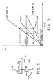
- FIG 3 is a waveform of voltage vs time useful in explaining the operation of the circuit of FIG. 1.
- FIG. 1 is a schematic diagram of a circuit for generating accurate timing pulses using FET devices which exhibit considerable parameter spreads as a result of manufacturing processes.
- the circuit includes a timer means 10, a reference and feedback amplifier means 12, a feedback difference amplifier means 14, a difference amplifier means 16 and a pulse shaper means 18.
- Timer means 10 includes an input transistor 20 connected to and triggered by a negative going waveform input signal.
- a depletion device 22 is connected between potential source V DD and transistor 20. This forms a constant current source which is triggered on by the input waveform signal and produces current i c .
- the current i c is applied to and charges capacitor 24 until a preset level is reached.
- FIG. 2 illustrates the current i c charging capacitor 24 to provide a voltage V x across capacitor 24.
- the d.c. reference voltage should be set high to intersect i c at point H on the same nominal time value line H-N-L whereas for smaller values of i c (i.e., SLOW) the d.c. reference voltage level should be set low to intersect i c at point L on the same nominal time value line H-N-L.
- a d.c. reference voltage V ref' will be generated to linearly vary with the changes in i c in order to maintain accurate (constant) timing.
- the varying reference voltage V ref' is generated by reference and feedback amplifier means 12.
- Reference and feedback amplifier means 12 includes a pair of transistors 26 and 28. Transistors 26 and 28 are connected between V DD and ground. Transistor 26 is electrically the same as transistor 22 which generates current i c , and the voltage V ref between transistors 26 and 28 is proportional to the current flowing through transistor 26. Thus, the voltage V ref is proportional to current i c . Thus, if i c is high as shown in FIG. 3, V ref will represent the error value H-N, whereas if i c is low, V ref will represent the error value N-L.
- the other five transistors 30, 32, 34, 36 and 38 of means 12 form a feedback amplifier to amplify V ref to a suitable value and provide stable gain and produces output d.c. voltage signal V ref' .
- the d.c. reference signal V ref' is applied to the gate of device 50 of feedback difference amplifier means 14.
- the output voltage signal of V x from constant current timing circuit 10 is applied to the gate of device 48 of feedback difference amplifier 14 which is a dynamic detector circuit including cross-coupled transistors 44 and 46, transistors 48 and 50 and transistor 52.
- Feedback difference amplifier circuit 14 is triggered and changes state when the voltage V x across capacitor 24 of constant current timing circuit 10 (which is proportional to i c ) equals the amplified reference voltage V ref' (i.e., the crossover point).
- the output signal from feedback difference amplifier means 14, which is the voltage at node 54 is applied to a straightforward difference amplifier means 16, including transistors 56, 58, 60, 62 and 64, for further amplification.
- the amplified output voltage signal from node 66 of difference amplifier means 16 is applied to a pulse shaper circuit means 18.
- Pulse shaper circuit means 18 includes a pair of depletion devices and transistors 72, 74 and 76. The same input signal applied to transistor 20 is also applied to the gate of transistor 72 and the output signal of difference amplifier 16 on node 66 is connected to the gate of transistor 76.
- the negative going input signal is applied to device 20, capacitor 24 charges in accordance with the rate of i c and an output voltage is provided from timer circuit 10 that is rising proportional to the rate of rise of i c . It may be faster than nominal or slower than nominal depending on the characteristics of the FET devices used. This rising voltage is appled to one side of difference amplifier 14 at the gate of device 48.
- V ref error signal V ref proportional to the current i c is produced which indicates whether i c is rising faster (H-N) or slower (N-L) then the desired nominal rise.
- V ref' is set such it is always at the same voltage value of the V x produced by i c at the end of the desired nominal time period, that is, for example, the time designated by the H-N-L line.
- This V ref' signal is applied to the other side of the difference amplifier 14 at the gate of device 50.
- Difference amplifier 50 will trigger when V x (due to i c from timer 10) is equal to the level of V ref' .
- the time when these voltages are equal is always the same time. If V x rises faster than nominal, then the V ref' produced is high, if V x rises slower than nominal then V ref' is low such that the two voltages are the same value along, for example, the H-N-L time line of FIG. 3.
- Difference amplifier triggers and produces a positive pulse at such time from device 48 and a corresponding negative pulse at this time from device 50 on node 54.
- Difference amplifier 14 is selected to have a wide input signal range and, therefore, has a low gain.
- the pulses from devices 48 and 50 are applied to another difference amplifier 16 to merely sharpen the pulse transitions and provide further amplification.
- a sharp negative going pulse is produced on node 66 which is applied to the base of device 76 of pulse shaper means 18.
- the negative going input signal is inverted by device 72 and turns on device 74.
- device 74 turns on the output voltage OUT from the pulse shaper means 18 goes low.
- the predetermined interval occurs corresponding to the signal at node 66 going negative.
- device 76 then goes off and the output voltage OUT goes high, completing the cycle. This provides an accurately timed clock pulse which always occurs at the same time regardless of variations in i c and V x due to variations in FET characteristics.
Landscapes
- Physics & Mathematics (AREA)
- Nonlinear Science (AREA)
- Manipulation Of Pulses (AREA)
- Pulse Circuits (AREA)
- Amplifiers (AREA)
Description
- The present invention relates to a circuit for generating accurate timing signals for computer clocking, and more particularly to a circuit including field effect transistor (FET) devices for producing accurate timing pulses.
- The prior art contains numerous references describing circuits of various types for providing timing signals or pulses. For example, U. S. Patent 3,969,719 issued July 13, 1976 to Sirocka et al entitled ELECTRONIC WATCH shows a circuit including an oscillator which produces reference pulses which are divided down and then applied to level converters and shaper circuits.
- U.S. Patent 3,935,475 issued January 27, 1976 to Margolies entitled TWO-PHASE MOS SYNCHRONIZER describes an input circuit to a clock pulse circuit which includes an FET logic circuit and an output circuit which includes an inverter in series with an FET.
- U.S. Patent 4,072,932 issued February 7, 1978 to Kitagawa et al entitled CLOCK GENERATOR FOR SEMICONDUCTOR MEMORY describes a timing generator circuit including a differential read clock generator consisting of an FET bistable amplifier and a differential voltage sensor.
- The prior art does not teach an FET clock generating circuit including a constant current timing circuit which feeds a reference and feedback amplifier, an output of which is connected to a feedback difference amplifier providing an output through a pulse shaper.
- Because of manufacturing processes, FET devices exhibit wide variations in parameters and tolerances, and it is therefore, difficult to utilize them in a clocking circuit where the generation of accurate timing pulses held to vary narrow tolerances is required.
- An object of the present invention is to provide a circuit using FET devices which will provide accurate timing pulses.
- Another object of the present invention is to provide an FET timing circuit including a constant current source that varies because of device variations and which further includes a reference voltage source which provides a compensating reference voltage that varies in level with the variations in the current source.
- Still another object of the present invention is to provide an FET timing circuit structure including a constant current source, a reference and feedback amplifier circuit for generating a varying reference voltage, a feedback difference amplifier for detecting the crossover between the constant current source signal and the reference voltage signal, and a pulse shaping circuit for providing an output timing signal adjusted in accordance with the crossover occurrence time.
- On Page 115 of EDN Volume 25, Number 2, published 20 January 1980, there is described a single-cycle timer integrated circuit connected to an external capacitor and resistor network. The capacitor and resistor are connected to a transistor switch to form a timing circuit responsive to a trigger pulse for producing a timing slope having a gradient depending on the values of circuit parameters and a supply voltage. A reference voltage generator in the form of a voltage divider generates a reference voltage having a magnitude proportional to the supply voltage. A detector connected to the timer circuit and the reference voltage generator produces a pulse signal representative of a cross-over time at which the magnitude of the timing slope is equal to that of the reference voltage. A flip flop is connected to the pulse signal and the trigger pulse for generating the output pulse.
- In accordance with the present invention, there is now provided a field effect transistor clock signal generator for providing an output clock signal adjusted in compensation for a variation in a transistor parameter comprising: a timer circuit responsive to an input clock pulse for producing a timing signal having a voltage slope which varies about a desired nominal slope in response to the variation in the transistor parameter; a reference voltage generator connected to the timer circuit for generating a reference voltage having a magnitude proportional to the difference between the voltage slope and the nominal slope; a difference amplifier connected to the timer circuit and the reference voltage generator for producing a pulse signal representative of a crossover time when the magnitude of the timing signal equals the magnitude of the reference voltage; a waveform shaper responsive to the input clock pulse and the pulse signal for producing an output clock pulse having an occurrence time determined by the input clock pulse and the crossover time; characterised in that: the timer circuit comprises a transistor current source connected between greater and lesser supply voltage levels for producing a current (Ic) in response to the input clock pulse, and a capacitor for generating the timing signal in response to the current (Ic); and the reference voltage generator comprises a first transistor matched to the transistor current source of the timer circuit and connected in series with a second transistor to form a voltage divider between the supply voltage levels for generating the reference voltage as a function of the current (Ic).
- The foregoing and other objects, features and advantages of this invention will be apparent from the following more particular description of the invention, as illustrated in the accompanying drawings.
- FIG. 1 is a schematic block diagram of a timing signal generator according to the principles of the present invention.
- FIG. 2 is a schematic illustration of the constant current timer portion of the circuit of FIG. 1.
- FIG 3 is a waveform of voltage vs time useful in explaining the operation of the circuit of FIG. 1.
- FIG. 1 is a schematic diagram of a circuit for generating accurate timing pulses using FET devices which exhibit considerable parameter spreads as a result of manufacturing processes. The circuit includes a timer means 10, a reference and feedback amplifier means 12, a feedback difference amplifier means 14, a difference amplifier means 16 and a pulse shaper means 18.
- Timer means 10 includes an
input transistor 20 connected to and triggered by a negative going waveform input signal. Adepletion device 22 is connected between potential source VDD andtransistor 20. This forms a constant current source which is triggered on by the input waveform signal and produces current ic. The current ic is applied to and chargescapacitor 24 until a preset level is reached. For example, FIG. 2 illustrates the current iccharging capacitor 24 to provide a voltage Vx acrosscapacitor 24. FIG. 3 illustrates the time for chargingcapacitor 24 to given levels of Vx. In a nominal time,capacitor 24 should charge to Vx=N for a nominal current ic. However, because of device manufacturing spreads, the current ic will vary, and for a spread as illustrated in FIG.3, a low value of ic will chargecapacitor 24 slowly such that Vx will only be equal L after the nominal time period and it will take until time F for Vx to reach the voltage line N. Likewise, a high value of ic will chargecapacitor 24 rapidly such that Vx will equal N at time S prior to the nominal time period and Vx will continue to increase and be as high as H after the nominal time period has elapsed. This variation is compensated for in the present invention by varying a d.c. reference voltage level linearly with the variation of current ic such that the time at which the voltage Vx acrosscapacitor 24 intersects the reference voltage level is maintained at a nominal constant value. In other words, referring to FIG. 3, the nominal time as measured to the line H-N-L should be maintained. Therefore, for large values of ic (i.e., FAST), the d.c. reference voltage should be set high to intersect ic at point H on the same nominal time value line H-N-L whereas for smaller values of ic (i.e., SLOW) the d.c. reference voltage level should be set low to intersect ic at point L on the same nominal time value line H-N-L. - Thus, as variations in the value of ic occur as a result of FET parameter spreads, a d.c. reference voltage Vref' will be generated to linearly vary with the changes in ic in order to maintain accurate (constant) timing. The varying reference voltage Vref' is generated by reference and feedback amplifier means 12.
- Reference and feedback amplifier means 12 includes a pair of
transistors 26 and 28.Transistors 26 and 28 are connected between VDD and ground. Transistor 26 is electrically the same astransistor 22 which generates current ic, and the voltage Vref betweentransistors 26 and 28 is proportional to the current flowing through transistor 26. Thus, the voltage Vref is proportional to current ic. Thus, if ic is high as shown in FIG. 3, Vref will represent the error value H-N, whereas if ic is low, Vref will represent the error value N-L. The other fivetransistors means 12 form a feedback amplifier to amplify Vref to a suitable value and provide stable gain and produces output d.c. voltage signal Vref'. - The d.c. reference signal Vref' is applied to the gate of
device 50 of feedback difference amplifier means 14. The output voltage signal of Vx from constantcurrent timing circuit 10 is applied to the gate ofdevice 48 offeedback difference amplifier 14 which is a dynamic detector circuit includingcross-coupled transistors transistors transistor 52. Feedbackdifference amplifier circuit 14 is triggered and changes state when the voltage Vx acrosscapacitor 24 of constant current timing circuit 10 (which is proportional to ic) equals the amplified reference voltage Vref' (i.e., the crossover point). - The output signal from feedback difference amplifier means 14, which is the voltage at
node 54 is applied to a straightforward difference amplifier means 16, includingtransistors node 66 of difference amplifier means 16 is applied to a pulse shaper circuit means 18. - Pulse shaper circuit means 18 includes a pair of depletion devices and
transistors transistor 20 is also applied to the gate oftransistor 72 and the output signal ofdifference amplifier 16 onnode 66 is connected to the gate oftransistor 76. - Referring now to FIG. 1, the negative going input signal is applied to
device 20,capacitor 24 charges in accordance with the rate of ic and an output voltage is provided fromtimer circuit 10 that is rising proportional to the rate of rise of ic. It may be faster than nominal or slower than nominal depending on the characteristics of the FET devices used. This rising voltage is appled to one side ofdifference amplifier 14 at the gate ofdevice 48. - Meanwhile,
device 20 of reference and feedback means 12 is connected todevice 22 oftimer 10 and an error signal Vref proportional to the current ic is produced which indicates whether ic is rising faster (H-N) or slower (N-L) then the desired nominal rise. This Vref voltage is amplied and made stable in the feedback amplifier portion ofmeans 12 and a d.c. output voltage Vref' is produced which is set high (i.e., at Vx=H of FIG. 3) when ic rises faster than nominal or is set low (i.e., Vx=L) when ic rises slower than nominal. In any case, Vref' is set such it is always at the same voltage value of the Vx produced by ic at the end of the desired nominal time period, that is, for example, the time designated by the H-N-L line. This Vref' signal is applied to the other side of thedifference amplifier 14 at the gate ofdevice 50. -
Difference amplifier 50 will trigger when Vx (due to ic from timer 10) is equal to the level of Vref'. The time when these voltages are equal is always the same time. If Vx rises faster than nominal, then the Vref' produced is high, if Vx rises slower than nominal then Vref' is low such that the two voltages are the same value along, for example, the H-N-L time line of FIG. 3. - Difference amplifier triggers and produces a positive pulse at such time from
device 48 and a corresponding negative pulse at this time fromdevice 50 onnode 54.Difference amplifier 14 is selected to have a wide input signal range and, therefore, has a low gain. The pulses fromdevices difference amplifier 16 to merely sharpen the pulse transitions and provide further amplification. Thus a sharp negative going pulse is produced onnode 66 which is applied to the base ofdevice 76 of pulse shaper means 18. - The same input negative going input signal applied to
device 20 of timer means 10 is applied to the base ofdevice 72 of pulse shaper means 18. - It should be recalled that the negative going pulse at
node 66 occurs at the desired nominal time because is is produced when Vx is equal to Vref'. - The negative going input signal is inverted by
device 72 and turns ondevice 74. Whendevice 74 turns on the output voltage OUT from the pulse shaper means 18 goes low. - Now the predetermined interval occurs corresponding to the signal at
node 66 going negative. When the signal atnode 66 goes negative,device 76 then goes off and the output voltage OUT goes high, completing the cycle. This provides an accurately timed clock pulse which always occurs at the same time regardless of variations in ic and Vx due to variations in FET characteristics.
Claims (5)
- A field effect transistor clock signal generator for providing an output clock signal adjusted in compensation for a variation in a transistor parameter comprising:
a timer circuit (10) responsive to an input clock pulse for producing a timing signal having a voltage slope which varies about a desired nominal slope in response to the variation in the transistor parameter;
a reference voltage generator (12) connected to the timer circuit (10) for generating a reference voltage having a magnitude proportional to the difference between the voltage slope and the nominal slope;
a difference amplifier (14) connected to the timer circuit (10) and the reference voltage generator (12) for producing a pulse signal representative of a crossover time when the magnitude of the timing signal equals the magnitude of the reference voltage;
a waveform shaper (18) responsive to the input clock pulse and the pulse signal for producing an output clock pulse having an occurrence time determined by the input clock pulse and the crossover time;
characterised in that:
the timer circuit (10) comprises a transistor current source (22) connected between greater and lesser supply voltage levels for producing a current (Ic) in response to the input clock pulse, and a capacitor (24) for generating the timing signal in response to the current (Ic);
and the reference voltage generator (12) comprises a first transistor (26) matched to the transistor current source (22) of the timer circuit (10) and connected in series with a second transistor (28) to form a voltage divider between the supply voltage levels for generating the reference voltage as a function of the current (Ic). - A clock signal generator as claimed in Claim 1 wherein the reference voltage generator (12) increases the reference voltage in response to the timing slope becoming greater than the nominal slope. and decreases the reference voltage in response to the timing slope becoming less than the nominal slope.
- A clock signal generator as claimed in Claim 2 wherein the reference voltage generator (12) comprises an amplifier (30,32,34,36,38) for amplifying the voltage level to generate a reference voltage for maintaining stability of the clock signal generator.
- A clock signal generator as claimed in Claim 3 wherein the feedback difference amplifier (14) comprises a first switching transistor (50) responsive to the reference voltage and a second switching transistor (48) responsive to the timing signal; the first and second switching transistors (50,48) being interconnected for generating the pulse signal when the magnitude of the timing signal and the magnitude of reference voltage are equal.
- A clock signal generator as claimed in Claim 4 wherein the pulse shaper (18) comprises first and second output transistors, the first output transistor turning on in response to the pulse signal, and the second output transistor turning on in response to the input clock pulse; the output clock pulse being produced when both the first and the second output transistors are turned on.
Applications Claiming Priority (2)
| Application Number | Priority Date | Filing Date | Title |
|---|---|---|---|
| US06/620,765 US4626705A (en) | 1984-06-14 | 1984-06-14 | Field effect transistor timing signal generator circuit |
| US620765 | 1984-06-14 |
Publications (3)
| Publication Number | Publication Date |
|---|---|
| EP0164616A2 EP0164616A2 (en) | 1985-12-18 |
| EP0164616A3 EP0164616A3 (en) | 1987-08-05 |
| EP0164616B1 true EP0164616B1 (en) | 1991-11-27 |
Family
ID=24487301
Family Applications (1)
| Application Number | Title | Priority Date | Filing Date |
|---|---|---|---|
| EP85106194A Expired EP0164616B1 (en) | 1984-06-14 | 1985-05-21 | Field effect transistor timing signal generator circuit |
Country Status (4)
| Country | Link |
|---|---|
| US (1) | US4626705A (en) |
| EP (1) | EP0164616B1 (en) |
| JP (1) | JPS614321A (en) |
| DE (1) | DE3584737D1 (en) |
Families Citing this family (5)
| Publication number | Priority date | Publication date | Assignee | Title |
|---|---|---|---|---|
| JPS6115676Y2 (en) * | 1979-11-16 | 1986-05-15 | ||
| JPS5680404A (en) * | 1979-12-07 | 1981-07-01 | Yoshitomi Pharmaceutical | Manufacture of antiseptically treated plywood |
| US5589784A (en) * | 1992-03-31 | 1996-12-31 | Texas Instruments Incorporated | Method and apparatus for detecting changes in a clock signal to static states |
| KR20000003558A (en) | 1998-06-29 | 2000-01-15 | 김영환 | Pulse generator |
| US8873270B2 (en) * | 2012-12-14 | 2014-10-28 | Palo Alto Research Center Incorporated | Pulse generator and ferroelectric memory circuit |
Family Cites Families (9)
| Publication number | Priority date | Publication date | Assignee | Title |
|---|---|---|---|---|
| US3365586A (en) * | 1965-05-20 | 1968-01-23 | Westinghouse Electric Corp | Miniaturized constant time delay circuit |
| US3969719A (en) * | 1973-01-02 | 1976-07-13 | Fairchild Camera And Instrument Corporation | Electronic watch |
| US3935475A (en) * | 1974-08-27 | 1976-01-27 | Gte Laboratories Incorporated | Two-phase MOS synchronizer |
| JPS5926136B2 (en) * | 1975-01-25 | 1984-06-25 | 日本電気株式会社 | clock regeneration circuit |
| US4072932A (en) * | 1976-08-23 | 1978-02-07 | Texas Instruments Incorporated | Clock generator for semiconductor memory |
| JPS53126548U (en) * | 1977-03-15 | 1978-10-07 | ||
| US4199693A (en) * | 1978-02-07 | 1980-04-22 | Burroughs Corporation | Compensated MOS timing network |
| JPS54144852A (en) * | 1978-05-04 | 1979-11-12 | Matsushita Electric Ind Co Ltd | Delay circuit |
| US4449059A (en) * | 1981-07-13 | 1984-05-15 | Tektronix, Inc. | Triangle waveform generator having a loop delay compensation network |
-
1984
- 1984-06-14 US US06/620,765 patent/US4626705A/en not_active Expired - Fee Related
-
1985
- 1985-02-08 JP JP60022144A patent/JPS614321A/en active Granted
- 1985-05-21 DE DE8585106194T patent/DE3584737D1/en not_active Expired - Lifetime
- 1985-05-21 EP EP85106194A patent/EP0164616B1/en not_active Expired
Also Published As
| Publication number | Publication date |
|---|---|
| US4626705A (en) | 1986-12-02 |
| EP0164616A2 (en) | 1985-12-18 |
| DE3584737D1 (en) | 1992-01-09 |
| JPS614321A (en) | 1986-01-10 |
| JPH0356485B2 (en) | 1991-08-28 |
| EP0164616A3 (en) | 1987-08-05 |
Similar Documents
| Publication | Publication Date | Title |
|---|---|---|
| US4496861A (en) | Integrated circuit synchronous delay line | |
| US5699024A (en) | Accurate integrated oscillator circuit | |
| EP1196993B1 (en) | Oscillator circuit | |
| KR100218975B1 (en) | Accuracy rc oscillator | |
| US5387882A (en) | Switched capacitor charge pump and sawtooth oscillator using same | |
| US4902910A (en) | Power supply voltage level sensing circuit | |
| EP0180105B1 (en) | Voltage controlled oscillator | |
| EP0377897A2 (en) | Duty ratio control circuit apparatus | |
| US4479097A (en) | Low voltage, low power RC oscillator circuit | |
| US4115748A (en) | MOS IC Oscillation circuit | |
| US4626705A (en) | Field effect transistor timing signal generator circuit | |
| US4370628A (en) | Relaxation oscillator including constant current source and latch circuit | |
| US4199693A (en) | Compensated MOS timing network | |
| US7952343B2 (en) | Current measurement circuit and method | |
| JPH01307312A (en) | Circuit for generating a series of pulses having predetermined and controlled impact coefficient | |
| US6271735B1 (en) | Oscillator controller with first and second voltage reference | |
| JPH0258806B2 (en) | ||
| CA1183582A (en) | Precision differential relaxation oscillator circuit | |
| CN117200700A (en) | Low-cost high-precision ring oscillator circuit and control method thereof | |
| EP0453083B1 (en) | An asynchronous delay circuit | |
| US5808484A (en) | Method and apparatus for detecting changes in a clock signal to static states | |
| US4413238A (en) | Precision differential relaxation oscillator circuit | |
| KR940010481A (en) | Low frequency oscillator | |
| US4554464A (en) | Propagation delay generator | |
| CN112667013B (en) | Current comparison type clock generation circuit and chip |
Legal Events
| Date | Code | Title | Description |
|---|---|---|---|
| PUAI | Public reference made under article 153(3) epc to a published international application that has entered the european phase |
Free format text: ORIGINAL CODE: 0009012 |
|
| AK | Designated contracting states |
Designated state(s): DE FR GB |
|
| 17P | Request for examination filed |
Effective date: 19860424 |
|
| PUAL | Search report despatched |
Free format text: ORIGINAL CODE: 0009013 |
|
| AK | Designated contracting states |
Kind code of ref document: A3 Designated state(s): DE FR GB |
|
| 17Q | First examination report despatched |
Effective date: 19890904 |
|
| GRAA | (expected) grant |
Free format text: ORIGINAL CODE: 0009210 |
|
| AK | Designated contracting states |
Kind code of ref document: B1 Designated state(s): DE FR GB |
|
| REF | Corresponds to: |
Ref document number: 3584737 Country of ref document: DE Date of ref document: 19920109 |
|
| ET | Fr: translation filed | ||
| PLBE | No opposition filed within time limit |
Free format text: ORIGINAL CODE: 0009261 |
|
| STAA | Information on the status of an ep patent application or granted ep patent |
Free format text: STATUS: NO OPPOSITION FILED WITHIN TIME LIMIT |
|
| 26N | No opposition filed | ||
| PGFP | Annual fee paid to national office [announced via postgrant information from national office to epo] |
Ref country code: GB Payment date: 19930427 Year of fee payment: 9 Ref country code: FR Payment date: 19930427 Year of fee payment: 9 |
|
| PGFP | Annual fee paid to national office [announced via postgrant information from national office to epo] |
Ref country code: DE Payment date: 19930525 Year of fee payment: 9 |
|
| PG25 | Lapsed in a contracting state [announced via postgrant information from national office to epo] |
Ref country code: GB Effective date: 19940521 |
|
| GBPC | Gb: european patent ceased through non-payment of renewal fee |
Effective date: 19940521 |
|
| PG25 | Lapsed in a contracting state [announced via postgrant information from national office to epo] |
Ref country code: FR Effective date: 19950131 |
|
| PG25 | Lapsed in a contracting state [announced via postgrant information from national office to epo] |
Ref country code: DE Effective date: 19950201 |
|
| REG | Reference to a national code |
Ref country code: FR Ref legal event code: ST |