EP0164584A1 - Sales registration apparatus - Google Patents
Sales registration apparatus Download PDFInfo
- Publication number
- EP0164584A1 EP0164584A1 EP85105780A EP85105780A EP0164584A1 EP 0164584 A1 EP0164584 A1 EP 0164584A1 EP 85105780 A EP85105780 A EP 85105780A EP 85105780 A EP85105780 A EP 85105780A EP 0164584 A1 EP0164584 A1 EP 0164584A1
- Authority
- EP
- European Patent Office
- Prior art keywords
- key
- data
- memory
- coupling means
- keyboard
- Prior art date
- Legal status (The legal status is an assumption and is not a legal conclusion. Google has not performed a legal analysis and makes no representation as to the accuracy of the status listed.)
- Granted
Links
Images


Classifications
-
- G—PHYSICS
- G06—COMPUTING; CALCULATING OR COUNTING
- G06Q—INFORMATION AND COMMUNICATION TECHNOLOGY [ICT] SPECIALLY ADAPTED FOR ADMINISTRATIVE, COMMERCIAL, FINANCIAL, MANAGERIAL OR SUPERVISORY PURPOSES; SYSTEMS OR METHODS SPECIALLY ADAPTED FOR ADMINISTRATIVE, COMMERCIAL, FINANCIAL, MANAGERIAL OR SUPERVISORY PURPOSES, NOT OTHERWISE PROVIDED FOR
- G06Q30/00—Commerce
- G06Q30/04—Billing or invoicing
-
- G—PHYSICS
- G06—COMPUTING; CALCULATING OR COUNTING
- G06Q—INFORMATION AND COMMUNICATION TECHNOLOGY [ICT] SPECIALLY ADAPTED FOR ADMINISTRATIVE, COMMERCIAL, FINANCIAL, MANAGERIAL OR SUPERVISORY PURPOSES; SYSTEMS OR METHODS SPECIALLY ADAPTED FOR ADMINISTRATIVE, COMMERCIAL, FINANCIAL, MANAGERIAL OR SUPERVISORY PURPOSES, NOT OTHERWISE PROVIDED FOR
- G06Q20/00—Payment architectures, schemes or protocols
- G06Q20/08—Payment architectures
- G06Q20/20—Point-of-sale [POS] network systems
-
- G—PHYSICS
- G06—COMPUTING; CALCULATING OR COUNTING
- G06Q—INFORMATION AND COMMUNICATION TECHNOLOGY [ICT] SPECIALLY ADAPTED FOR ADMINISTRATIVE, COMMERCIAL, FINANCIAL, MANAGERIAL OR SUPERVISORY PURPOSES; SYSTEMS OR METHODS SPECIALLY ADAPTED FOR ADMINISTRATIVE, COMMERCIAL, FINANCIAL, MANAGERIAL OR SUPERVISORY PURPOSES, NOT OTHERWISE PROVIDED FOR
- G06Q20/00—Payment architectures, schemes or protocols
- G06Q20/30—Payment architectures, schemes or protocols characterised by the use of specific devices or networks
- G06Q20/34—Payment architectures, schemes or protocols characterised by the use of specific devices or networks using cards, e.g. integrated circuit [IC] cards or magnetic cards
- G06Q20/342—Cards defining paid or billed services or quantities
-
- G—PHYSICS
- G07—CHECKING-DEVICES
- G07F—COIN-FREED OR LIKE APPARATUS
- G07F7/00—Mechanisms actuated by objects other than coins to free or to actuate vending, hiring, coin or paper currency dispensing or refunding apparatus
- G07F7/02—Mechanisms actuated by objects other than coins to free or to actuate vending, hiring, coin or paper currency dispensing or refunding apparatus by keys or other credit registering devices
- G07F7/025—Mechanisms actuated by objects other than coins to free or to actuate vending, hiring, coin or paper currency dispensing or refunding apparatus by keys or other credit registering devices by means, e.g. cards, providing billing information at the time of purchase, e.g. identification of seller or purchaser, quantity of goods delivered or to be delivered
-
- G—PHYSICS
- G07—CHECKING-DEVICES
- G07G—REGISTERING THE RECEIPT OF CASH, VALUABLES, OR TOKENS
- G07G1/00—Cash registers
- G07G1/12—Cash registers electronically operated
Abstract
Description
- The present invention relates to a sales registration apparatus which performs sales registration processing with respect to items for sale in accordance with various fixed control data set in an internal memory and, more particularly, to a sales registration apparatus which can simplify the operation for setting various fixed control data in the memory.
- In sales registration apparatuses such as terminals of a POS (Point-Of-Sales) system in large retail stores, e.g., department stores, supermarkets and the like and electronic cash registers in small retail stores, sales registration files for registering sales data of items such as price, number, department code data, and the like entered by operating registration keys provided on a keyboard are stored in an internal memory unit.
- Even if the sales registration apparatuses having the same specifications are used, contents of these sales registration files differ in accordance with a size of the POS system, types of items to be sold, a difference in methods for totaling sales or in demands of users. Generally, sales registration apparatuses are manufactured to have the same specifications, and when the apparatus is delivered or located on a certain sales floor designated by the user, the sales registration files required by the user are set in the internal memory of the apparatus.
- However, in order to reduce manuacturing cost, the sales registration apparatus of this type does not comprise a specific interface for automatically inputting various fixed control data such as department code, name of item, price for each department, item code which constitute the sales registration files. Therefore, when the fixed data are set in the internal memory, they must be entered by operating keys provided on a keyboard for each step in a predetermined procedure. For this reason, when a plurality of sales registration apparatuses are to be delivered to a single user or when those having the same registration file content are delivered to different users, fixed control data must be set by operating keys on the keyboard for each apparatus. As a result, the overall time required for setting fixed control data is increased, and fixed control data can be erroneously set.
- It is an object of the present invention to provide a sales registration apparatus in which fixed control data stored in a detachable type data setting device can be transferred to an internal memory.
- In order to achieve the above object of the present invention, there is provided a sales registration apparatus comprising first and second coupling units detachably coupled to each other; a keyboard, coupled to the first coupling unit and including numeral setting keys and department keys, for supplying through the first coupling unit key-in signals corresponding to a key operation in response to key-out signals supplied through the first coupling unit; a first memory; a first control unit, coupled to the second coupling unit, for supplying the key-out signals through the second coupling unit and for writing a control program and sales registration data in the first memory in response to the key-in signals supplied through the second coupling unit; a second memory for sequentially storing key data corresponding to key-in signals; an operation mode setting section; a third coupling unit detachably coupled to the second coupling unit; and a second control unit, coupled to the third coupling unit, for sequentially transferring the key data from the second memory to the first control unit through the third ana second coupling units in a programming mode to cause the key data to be stored in the first memory.
- According to the present invention, when the data setting device is coupled, e.g., to a cash register and is set in a programming mode, key data stored in the second memory of the data setting device can be transmitted to and stored in the first memory of the cash register. Therefore, the identical key data can be easily and quickly stored in the memory of the cash register.
- This invention can be more fully understood from the following detailed description when taken in conjunction with the accompanying drawings, in which:
- Fig. 1 is a perspective view of a data setting device used in a sales registration apparatus according to an embodiment of the present invention;
- Fig. 2 is a schematic view of the sales registration apparatus comprising a cash register and the data setting device connected to each other;
- Fig. 3 shows a keyboard of the cash register shown in Fig. 2;
- Fig. 4 is a block diagram of a control circuit of the cash register shown in Fig. 2;
- Fig. 5 is a memory map of a RAM used in the control circuit shown in Fig. 4;
- Fig. 6 is a circuit diagram of the keyboard, a keyboard control circuit, and a control circuit of the data setting device;
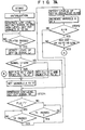
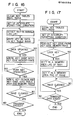
- Figs. 7A, 7B and 8 are flow charts for explaining an operation of the control circuit of the cash register shown in Fig. 4;
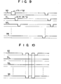
- Figs. 9 and 10 are flow charts for explaining an operation of the control circuit of the cash register shown in Fig. 4;
- Figs. 11 and 12 are circuit diagrams of a keyboard, a keyboard control circuit, and a data setting device according to another embodiment of the present invention;
- Fig. 13 is a memory map of a RAM of the data setting device shown in Fig. 12; and
- Figs. 14 to 19 are flow charts for explaining an operation of the control circuit of the data setting device shown in Fig. 12.
- Fig. 1 is a perspective view of a
data setting device 11 of a sales registration apparatus according to an embodiment of the present invention. Thedevice 11 comprises a box-shaped casing 1 containing various electronic components therein, four lock-type operation switches 4 to 7, three push-buttontype control keys 8 to 10, asocket 2 to which a programmable read-only memory (P-ROM) is detachably connected, and connectingterminal unit 3 provided on an upper surface of thecasing 1 and detachably coupled to a keyboard of an electronic cash register through a cable. - The four operation switches are a program (PR)
switch 4 for designating an operation mode of writing a sales registration file or a program to a key code memory, a setting (ES)switch 5 for designating an operation mode of setting the program to the cash register, a write (RW)switch 6 for designating an operation mode of writing a stored content of the key code memory in the P-ROM, and a read (RR)switch 7 for designating an operation mode of reading out a key code written in the P-ROM, respectively. The three control keys are a start (ST)key 8 for designating the start of the respective operations, a stop (SP)key 9 for designating a forced stop of the operations, and an all clear (AC)key 10 for clearing a storage content of a storage unit such as the key code memory. A connectingterminal unit 12 is detachably connected to the connecting terminal of a keyboard control circuit of the cash register through acable 13. - Fig. 2 shows a state wherein the
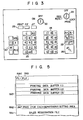
program setting device 11 is connected to acash register 14. When a program is set in thedata setting device 11 orcash register 14, acover 17 is removed covering aprinter 16 adjacent to akeyboard 15 on a front surface of theregister 14. A connecting terminal unit 15CT which is connected at one end to acable 18 extending from a back surface of thekeyboard 15 and which is usually connected at the other end to the connecting terminal unit of the keyboard control circuit is disconnected from the connecting terminal unit of the keyboard control circuit and then connected to theterminal unit 3 of thedevice 11. The connecting terminal unit of the keyboard control circuit is connected to a connectingterminal unit 12 of thedevice 11. Note that adisplay unit 20 of thecash register 14 is used to display a unit price or a total price. - As shown in Fig. 3, the
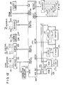
keyboard 15 comprisesnumeral setting keys 23 for setting sales prices and the number of items,department keys 24 indicating classifications of the items, a subtotal key 25, a charge/cashtotal key 26 for calculating a total amount of the sale,various function keys 27 such as cancel and PLU keys, aprint switch 28 for designating a print output of the fixed control data set in the storage unit, and the like. Furthermore, thekeyboard 15 is provided with acontrol switch 29 and apower switch 30 which are operated by a key. Thecontrol switch 29 is used to designate respective operations of "registration", "program", "reset" so as to cause a central processing unit to execute them. In the "registration" operation, department codes of the items and sales data of a sales price are registered in a sales registration file formed in the storage unit, and the total amount of the sale is calculated so that the result is printed on journal paper by theprinter 16. In the "program" operation, fixed control data such as the department code, the unit price determined for each department, names of items and the like are preset in the sales registration file. Furthermore, in the "reset" operation, for example, when the operations for a day is completed, a total sales amount and the total number of items sold accumulated in the sales registration file is printed on the journal paper as a calculation report. - Fig. 4 is a block diagram of the sales registration apparatus according to the embodiment of the present invention. The apparatus comprises a central processing unit (CPU) 50, a read-only memory (ROM) 52 for storing a program to be executed by the
CPU 50, and a random- access memory (RAM) 54 for storing key code data and the like corresponding to key-in signals supplied from thekeyboard 15 of thecash register 14. Furthermore, thekeyboard 15, theprinter 16, thedisplay unit 20, and thecontrol switch 29 are connected to theCPU 50 respectively through akeyboard control circuit 56, aprinter driver 58, adisplay driver 60 and an I/O port 62. As will be described later, thedata setting device 11 is detachably coupled between thekeyboard 15 and thecontrol circuit 56. - As shown in Fig. 5, the
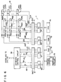
RAM 54 includes a sales registration file RAl for totaling sales data supplied by key operations on thekeyboard 15, e.g., for each department code, a unit price (for each department) setting area RA2 for storing a unit price determined for each department set in respective department code areas in the file RAl, and printing data buffers RA3 for temporarily storing data for one line to be printed on the journal paper by theprinter 16. In addition to these, theRAM 54 includes a memory area RA4 for storing a delay flag FL1 which designates a delay time Tl when thekeyboard 15 is directly connected to thecontrol circuit 56, that is, when the connecting terminal unit 15CT is directly connected to that of thecircuit 56, and a memory area RA5 for storing a delay flag FL2 which designates a delay time T2 when the connectingterminal unit 12 of thedevice 11 is connected to thecircuit 56. Note that thetime T2 is set to be longer than the time Tl. - Fig. 6 is a circuit diagram showing a main part of the sales registration apparatus when the
device 11 is connected to thecircuit 56. Thedevice 11 comprises aCPU 70, aROM 72 for storing a program for theCPU 70, aRAM 74 connected to a back-up battery and having an internal key code memory for storing key data corresponding to key-in signals from thekeyboard 15 as the fixed control data in a key code format, a switch control unit 76 receiving a command signal from a switching circuit 78 including the above-mentionedcontrol switches 4 to 7, and I/O ports 79 to 82. - (N+l) key-out signals SO to SN generated from the
circuit 56 are supplied to the I/O port 82 through a connecting terminal unit 56CT provided on thecircuit 56, and theconnecting terminal unit 12 provided on thedevice 11. Each of key-out signals KSO to KSN having substantially the same waveform as that of the key-out signals SO to SN supplied to the I/O port 82 is supplied from the I/O port 80 to corresponding commonly connected nodes of push keys PKOO to PKN5 arranged in a [6X(N+1)]-matrix form and lock keys LK00 to LKN1 arranged in a [2X(N+l)]-matrix form in thekeyboard 15 through the connectingterminal 3 and 15CT. - The push keys correspond to registration keys such as the
keys print switch 28. Other lock keys correspond to thecontrol key 29 for designating various operations. - Assume now that the
program switch 4 is turned ON, and that key-in signals PRO to PR5 obtained from the keys PKOO to PKN5 and key-in signals LRO and LR1 obtained from the lock keys LKOO to LKN1 are supplied to the I/O port 79 in thedevice 11 through the connecting terminal units 15CT and 3. Then, key-in signals PO to P5, LO and L1 having substantially the same waveform as that of the key-in signals PRO to PR5, LRO and LR1 are supplied from the I/O port 81 of thedevice 11 to thecircuit 56 through the connectingterminal units 12 and 56CT. Note that the data setting device is so designed that, when the key-out signal SO generated from thecircuit 56 is at LOW level, theCPU 70 of thedevice 11 supplies the signal Ll of LOW level to thecircuit 56 through the I/O port 81 as if the imaginary lock key LK01 were turned on. Simultaneously, key code data corresponding to the operation states of the push keys and the lock keys of thekeyboard 15 represented by the key-in signals PRO to PR5, LRO and LR1 from thekeyboard 15 is written in the key code memory of theRAM 74 in each key operation, and thus a plurality of key code data are successively written in the key code memory in accordance with an operation procedure of thekeyboard 15. - With this arrangement, when the
power switch 30 is turned on and thecash register 14 and thedata setting device 11 are supplied with a power source voltage, theCPU 50 of the apparatus shown in Fig. 4 executes the operation of setting the fixed control data in theR AM 54 in accordance with the flow charts shown in Figs. 7A, 7B and 8. When theswitch 30 is turned on, theCPU 50 performs initialization step with respect to respective storage units, and thereafter sets the key-out signal SO to LOW level and the key-out signals Sl to SN to HIGH level which are supplied from thekeyboard control circuit 56. When a total time (Tl+T2) of the delay flags FL1 and FL2 in the memory areas RA4 andR A5 of theRAM 54 has passed, theCPU 50 detects the level of the key-in signal Ll on a line to which the imaginary lock key LK01 is connected among the key-in signals supplied to thecircuit 56. If, at this time, theCPU 50 detects that the signal Ll is at LOW level, since the LOW level signal Ll can be generated at this time from thedevice 11, theCPU 50 determines that thedevice 11 is connected to thecircuit 56. Thus, theCPU 50 sets "1" in the delay flag FL2 of the area RA5, and resets the delay flag FL1 of the area RA4 to "0". However, when the key-in signal Ll is at HIGH level, since this HIGH level key-in signal can be supplied at this time from thekeyboard 15 through the terminal unit 15CT and 56CT without passing through thedevice 11, theCPU 50 determines that thedevice 11 is not connected to thecircuit 56. Thus, theCPU 50 resets the flag FL2 of the area RA5 to "0" and sets "1" in the flag FL1 of the area RA4. - After the
CPU 50 determines whether or not thedevice 11 is connected to thecircuit 56, theCPU 50 sets a variable A indicating the number of one of the signals SO to SN at "0". InSTEP 1, theCPU 50 sets the Ath key-out signal SA at LOW level which is then supplied from the terminal unit 56CT. Then, theCPU 50 checks the status of the flag FL2 of the area RA5, and if the flag LF2 is at "I", since this indicates that thedevice 11 is connected to thecircuit 56, theCPU 50 detects the levels of the signals PO to P5 supplied through the terminal unit 56CT after the time T2 has passed. Note that if the flag FL2 is at "0", since this indicates that thekeyboard 15 is directly connected to thecircuit 56, theCPU 50 detects the levels of the signals PO to P5 after the time Tl shorter than the time T2 has passed. Thereafter, theCPU 50 increments the variable A by one, and inSTEP 2, it checks if the variable A has reached a limit value N. If it is NO inSTEP 2, the flow returns to STEP 1. Then, inSTEP 1, theCPU 50 sets the next key-out signal SA at LOW level and causes the LOW level key-out signal SA to be generated through the connecting terminal unit 56CT. Thereafter, theCPU 50 detects the levels of the key-in signals. When theCPU 50 detects that A = N inSTEP 2, it determines that the operation of fetching key data caused by operation of the keys PKOO to PKN5 is completed. Thus, theCPU 50 checks if any one of the key-in signals PO to P5 includes LOW level data indicating that the keys are actually depressed. - When the
CPU 50 detects that any one of tne key-in signals PO to P5 is set at LOW level, it checks if the flag FL2 is at "1" inSTEP 3. When the flag FL2 is "0", i.e., when thekeyboard 15 is directly connected to thecircuit 56, theCPU 50 checks if a memory area for writing data of the area RA3 in theRAM 54 is available. If it is NO in this step, theCPU 50 executes error processing. However, when the status discrimination of the flag FL2 is completed, theCPU 50 sets the variable A at "0", and generates the LOW level signal SA in the same manner as described above. Then, after the time Tl or T2 corresponding to the status of the flag FL2 has passed, theCPU 50 detects the levels of the key-in signals LO and Ll corresponding to the states of the lock keys. - Thereafter, the
CPU 50 increments the variable A by one, and when it is detected that the variable A reaches the value N, in STEP4, theCPU 50 determines that all the data supplied according to the states of the keys LKOO to LKN1 and the keys PKOO to PKN5 have been fetched. Then, theCPU 50 starts to execute a data processing routine shown in Fig. 8. In the data processing routine, when theCPU 50 detects based on the key-in signals L0 and Ll from the lock keys that thecontrol switch 29 is set in the program mode, and detects based on the signals PO to P5 from the push keys that the data is supplied by operation of thedepartment keys 24, theCPU 50 then determines that the programming operation corresponds to the operation of programming unit prices for respective departments. TheCPU 50 sets in the area RA2 of the file RAl the unit price data for each department supplied by thenumeral setting keys 23 which were operated before a key operation of thedepartment key 24. Thereafter, theCPU 50 checks the status of the lock key LKll, i.e., if theprint switch 28 is turned on. When theswitch 28 is turned on, theCPU 50 determines that the unit price data must be printed. Then, theCPU 50 checks if a memory area for storing the unit price data for each department in the area RA3 is available. When the memory area is not available, theCPU 50 causes theprinter 16 to print out the data already stored in the memory area RA3 and stores the current unit price data therein. - After the unit price for each department is set in the memory area RA2, the
CPU 50 determines that the 'operation of setting one fixed control data in theRAM 54 is completed. Thus, theCPU 50 generates, as a synchronizing signal, a key-in reception signal, which includes the key-out signal SO having three LOW level pulses of pulse width T3 and the key-out signal SN having two LOW level pulses with the other key-out signals kept at LOW level as shown in Fig. 10. Then, theCPU 50 ends the programming operation for one fixed data. Thereafter, theCPU 50 resets the variable A to "0" and the flow returns to STEP 1. - In the sales registration apparatus having the above arrangement, suppose that the
device 11 is connected to the terminal unit 56CT of thecircuit 56, as shown in Fig. 1, and that thedata setting switch 5 is turned ON to transfer the various fixed control data prestored in the key code area of theRAM 74 of thedevice 11 to theRAM 54 of thecircuit 56. In this case, the key-in reception signal shown in Fig. 10 is supplied to thedevice 11 every time one fixed control data is supplied to thecircuit 56. Therefore, when thedevice 11 receives the reception signal, since it means that thekeyboard control circuit 56. is ready for receiving the next data from thedevice 11, the fixed control data stored in the key code memory of theRAM 74 can be sequentially and automatically set in theRAM 54 of thecash register 14, thus decreasing the overall time required for data setting. Since the reception signal is generated for each data reception, the data will not be erroneously set. - When the
device 11 is connected to thecash register 14, since a time (delay time) after the key-out signals are generated from thecircuit 56 until the levels of the key-in signals corresponding to the key-out signals are all detected is set to be longer, data setting can be ensured when thedevice 11 is used. - The
print switch 28 provided on thekeyboard 15 of the apparatus can be preset to determine whether or not the data is to be printed on the jounal paper by theprinter 16 when fixed control data is set in theRAM 54. of the apparatus. Thus, when fixed control data is set using thedevice 11, the setting efficiency can be improved by omitting a print out operation. - In a case where the fixed control data from the
device 11 is set in theRAM 54 and where the data is to be printed upon setting of the data, the data can be written into theRAM 54 even if the printing data buffer does not have an available area. Then, the data is temporarily stored in theRAM 54, and when an available area is obtained in the buffer, the data is stored therein. Therefore, fixed control data can be reliably stored in theRAM 54. - When the
device 11 is connected to thecircuit 56, since this can be automatically detected by the key-in signal Ll supplied from thedevice 11, an erroneous operation can be prevented in the data setting mode. - Fig. 11 shows a modification of the
keyboard 15, thekeyboard control circuit 56 and thedata setting device 11 shown in Fig. 6, and Fig. 12 is a detailed circuit diagram of the data setting circuit shown in Fig. 11. In this case, other components such asCPU 50,ROM 52,RAM 54 shown in Fig. 4 can be used in the second embodiment, and theCPU 50 functions in substantially the same manner as described with reference to Figs. 7A, 7B, 8 to 10. Referring to Fig. ll, adecoder 56D of thecircuit 56 generates key-out signals SO to SN through connecting terminal units 56CT and 12 in accordance with control data from akey control unit 56K. Furthermore, thecircuit 56 comprises apower source 56P for supplying a power source voltage to circuit components of thecash register 14 and to a power source line PSL through the terminals 56CT and 12. - As shown in Fig. 12, the
device 11 comprises a microprocessor (CPU) 100 including a plurality of input and output ports. A data bus 102 and anaddress bus 104 of theCPU 100 are connected to aROM 106 for storing a control program of thedevice 11 and aRAM 108 for storing data such as key code data supplied from thekeyboard 15 of thecash register 14. Thebuses 102 and 104 are connected to a P-ROM 109 connected to asocket 2 of acasing 1 respectively throughlatches 110 and 112. Atristate buffer 114 is connected between the P-RO M 109 and the bus 102. - Respective operation switches 4 to 7 and
control switches 8 to 10 are connected between an output port (C) and an input port (C) of theCPU 100 through adecoder 116. A clock terminal CLK receives a clock signal from a clock generator 118. - (N+l) key-out signals SO to SN generated through the
keyboard control unit 56K, which is connected to acontrol unit 50 of-thecash register 14 havingmemories encoder 120 through the terminal unit 56CT of thecash register 14 and theterminal unit 12 of thedevice 11. Output data from theencoder 120 is directly supplied to an input port (A) of theCPU 100 and is also supplied to atransition detector 122. When at least one bit of the output data from theencoder 120 is changed, thedetector 122 supplies an interrupt signal to an input terminal INTR of theCPU 100 which in turn receives the data from theencoder 120. - Signals corresponding to the output data from the
encoder 120 supplied to the input port (A) of theCPU 100 are supplied to adecoder 124 from an output port (B) of theCPU 100. Thedecoder 124 converts the input signals into (N+l) key-out signals KSO to KSN having the same waveform as that of the key-out signals SO to SN from thedecoder 56D, and are each supplied through theterminal units 3 of thedevice 11 and the terminal unit 15CT of thecash register 14 to corresponding commonly connected ends of push keys PKOO to PKNN arranged in an [(N+1)x(N+1)] matrix and lock keys LKOO to LKN1 arranged in an [(N+1)x2] matrix. - Key-in signals PRO to PRN obtained from the other ends of the push keys PKOO to PKNN and key-in signals LRO and LR1 obtained from the other ends of the lock keys LKOO to LKN1 are supplied to an input port (B) of the
CPU 100 through the terminal units 15CT and 3. - The power source voltage generated from the
power source 56P of thecash register 14 is supplied to apower circuit 130 of thedevice 11 through the terminal units 56CT and 12. A circuit operation voltage VD and a write voltage VP for the P-ROM 109 are generated from thepower circuit 130. - The
RAM 108 includes a key table RAX1 having one-bit memory areas LXOO to LXN1 for storing an operating states of the lock keys LKOO to LKN1 of thekeyboard 15 of thecash register 14, a key table RAX2 having one-bit memory areas PXOO to PXNN for storing operating states of the push keys PKOO to PKNN, and a key code memory area RAX3 for sequentially storing key code data each representing the operating states of the respective keys PKOO to PKNN and LKOO to LKNl obtained in each key operation cycle, as shown in Fig. 13. - With this arrangement, (N+l) key-out signals SO to SN having phases slightly shifted from each other as shown in Fig. 9 are generated from the
keyboard control circuit 56 of thecash register 14 through thedecoder 56D. The signals SO to SN are converted into output data EO by theencoder 120 in thedata setting device 11, and are supplied to the input port (A) and thetransition detector 122. Every time the output data EO is changed, thedetector 122 supplies its output pulse signal as the interrupt signal to the input terminal INTR of theCPU 100. In response to the interrupt signal, theCPU 100 receives the data EO and supplies signals corresponding to the output data EO to thedecoder 124 from the output port (B). Then, thedecoder 124 supplies to thekeyboard 15 the key-out signals KSO to KSN having the same waveform as that of the key-out signals generated from thedecoder 56D. Therefore, when the push keys and lock keys are depressed, the key-in signals PRO to PRN, LRO and LR1 representing the depressed keys are supplied to the input port (B) of theCPU 100. - In this manner, when various signals are supplied from the
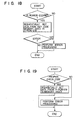
circuit 56 and thekeyboard 15 of thecash register 14, theCPU 100 of thedevice 11 executes a data setting operation with respect to thecash register 14 in accordance with the flow chart shown in Fig. 14. More specifically, when thedevice 11 is powered, theCPU 100 checks if the start (ST)key 8 is depressed. If it is YES in this step, theCPU 100 checks which of the operation switches 4 to 7 is selected, and executes an operation designated by the selected switch. Every time an interrupt signal DO is supplied to the interrupt input terminal INT of theCPU 100, theCPU 100 executes interruption processing. - Referring to Fig. 15, when the interrupt signal DO is supplied, the
CPU 100 detects the level of the key-in signals supplied to the input port (B) thereof from thekeyboard 15, and reads the corresponding data indicating the operating states of the push keys or lock keys from the tables RAX1 and RAX2. The readout data are transmitted from the output port (A) to thekeyboard control circuit 56 of thecash register 14 through thebuffer 126 and theterminal unit 12 as key-in signals PO to PN, LO and Ll having the same waveform as that of the key-in signals PRO to PRN, LRO and LR1 from thekeyboard 15. When all the key-in signals PO to PN, LO and Ll have been transmitted to thecircuit 56, theCPU 100 waits for a sync signal indicating reception of the key-in signals. When the sync signal is supplied, theCPU 100 clears the key table RAX2 of the push keys of theRAM 108, and the flow ends. - Referring again to Fig. 14, if the depressed operation switch is the program (PR)
switch 4, theCPU 100 executes programming process shown in Fig. 16. More specifically, theCPU 100 clears the key tables RAX1 and RAX2 so as to set up an interrupt permitting condition in which interruption processing shown in Fig. 15 can be executed. Then, theCPU 100 detects the ON/OFF state of the lock keys in accordance with the levels of-the key-in signals LRO and LR1 supplied to the input port (B) thereof. For example, when a lock key LKij is turned on, theCPU 100 sets "1" in a corresponding memory area LXij, and when the lock key LKij is turned off, it sets "0" in the memory area LXij. When the key-in data is different from the previous data stored, theCPU 100 determines that the data in this memory area has been updated, and writes the key code in the next available memory area of the key code memory RAX3. Similarly, theCPU 100 checks the ON/OFF states of the push keys in accordance with the key-in signals PRO to PRN. When a push key PKij is depressed, theCPU 100 sets "1" in a corresponding memory area PXij of the table RAX2, and writes the key code of the corresponding push key in the next available memory area of the key code memory RAX3. Note that, in this case, each time an interrupt signal is generated from thetransition detector 122, theCPU 100 writes data correspnding to the levels of the key-in signals PRO to PRN, or key-in signals LRO and LRN into the memory areas PXiO to PXiN, or memory areas LXiO and LXil, and writes corresponding key code data into a next available memory area of thememory RAX 3. Then, theCPU 100 stands by until the table RAX2 is cleared by the interruption processing of Fig. 15. When the table RAX2 is cleared, theCPU 100 determines that the key code data corresponding to one key operation has been written in the memory RAX3, and stands by for the next key operation. When all the key operations are completed and the program to be written ends, the flow ends. At this time, a plurality of key code data are stored in the memory RAX3 in a sequence determined by the sequence of the key operations. - Referring to Fig. 14, when the depressed operation switch is the setting (ES)
switch 5 for setting the storage content of the memory RAX3 in theRAM 54 of theregister 14, theCPU 100 executes program transferring processing in Fig. 17. In the same manner as in the processing in Fig. 16, theCPU 100 clears the tables RAX1 and RAX2 so as to set them in the interrupt permitting condition, and thereafter reads one key code from the memory RAX3. The readout sequence is the same as the sequence in which the key codes are written in. TheCPU 100 checks if the readout key code indicates a lock key. If the key code indicates a lock key, theCPU 100 sets "1" in the corresponding memory area LXij of the table RAX1. However, in this case, when the corresponding memory area is already set at "I", the area is cleared to "0". If the key code does not indicate a lock key, since it indicates a push key, theCPU 100 sets "1" in the corresponding memory area PXij of the table RAX2, and stands by until the table RAX2 is cleared by the interruption processing of Fig. 15. Note that, in this case, each time an interrupt signal is generated, theCPU 100 writes data corresponding to the key code into the memory areas PXiO to PXiN or memory areas LXiO and LXil and then transfers the data to theCPU 50 of thecash register 14. In this manner, when data corresonding to the key code read out from the memory RAX3 is selectively set in the table RAXI or RAX2 and is supplied to thecircuit 56 of thecash register 14, theCPU 100 reads out the next key code. When all the key codes have been transferred to thecircuit 56, the flow ends. - Referring to Fig. 14, when the depressed operation switch is the write (PW) switch 29 indicating a write operation of the storage content of the memory RAX3 in the P-
ROM 109, theCPU 100 executes write-in processing for the P-ROM 109 shown in Fig. 18. TheCPU 100 checks if the P-ROM 109 is properly connected to thesocket 2 of thecasing 1 and if the storage content thereof is erased. Thereafter, theCPU 100 sequentially reads out the key codes stored in the memory RAX3 so as to write them in the P-ROM 109. In this case, the voltage VP required for the write operation can be applied to a voltage input terminal of the P-ROM 109 while holding addresses and data in thelatches 110 and l12 for a time required therefor. When the write operation of the key codes in the P-ROM 109 is completed, theCPU 100 checks if the codes are normally written, and if there is no error, the flow ends. - Referring to Fig. 14, when the depressed operation switch is the read (RR)
switch 7 indicating a read operation for reading out a program, i.e., the key codes written in the P-ROM 109, theCPU 100 executes the readout processing shown in Fig. 19. TheCPU 100 checks that a check code of the P-ROM 109 is correct, and thereafter, reads out the key codes stored in the P-ROM 109 so as to write them in the keycode memory R AX3 of theRAM 108. In this case, addesses are supplied through the latch 112, and thebuffer 114 is activated by a control signal generated from a control terminal CNT(A), thereby supplying the key codes to the data bus 102 through thebuffer 114. In this manner, theCPU 100 fetches the key codes on the data bus 102 and writes them in the memory RAX3 of theRAM 108. - In the
data setting device 11, the key-out signals KSO to KSN supplied to thekeyboard 15 of thecash register 14 have substantially the same waveform as that of the key-out signals SO to SN generated from thecircuit 56 of theregister 14 through thedecoder 56D, and the key-in signals PO to PN, LO and Ll supplied to thecircuit 56 have substantially the same waveform as that of the key-in signals PRO to PRN, LRO and LR1 generated from thekeyboard 15. Therefore, when thedevice 11 is connected, thecash register 14 need not be modified and the control program thereof also need not be changed. Therefore, when the program is directly set in theregister 14 and it is written in thedevice 11, since the key operation of thekeyboard 15 can be the same, no specific training for using thedevice 11 is required. Note that in the above embodiment, the program can be simultaneously set both in theregister 14 and thedevice 11. - Since the
keyboard 15 and thekeyboard control circuit 56 are detachably connected to each other through the connecting terminals 15CT and 56CT, thedevice 11 can be easily inserted therebetween, thus decreasing the time required for setting the program. - Once the program is written in the key code memory RAX3 of the
RAM 108 of thedevice 11 by key-in operations from thekeyboard 15, the same program can be easily set in the storage unit of another cash register in such a manner that the connecting terminals of thecircuit 56 are connected to theterminals 12 of thedevice 11 and the settingswitch 5 is turned on. Therefore, the program need not be set by key-in operations from the keyboard for each cash register. As a result, the total time required for the program setting operation can be shortened, and the setting of erroneous data can be effectively prevented. - In the above embodiments, since the program which is written in the memory RAX3 of the
RAM 108 of thedevice 11 can be written in the P-ROM 109, the basic program can be kept. Furthermore, since the P-ROM 109 is easily detachable from thesocket 2 provided on the upper surface of thecasing 1, when several types of P-ROMs are prepared, the time for the program setting operation can be further shortened. - Since power for driving respective electronic components is supplied from the
cash register 14 to which the program is to be set, the program setting device requires no primary power source circuit of an AC power source, and it can be light in weight and low in cost. Particularly, when the program setting devices are used in an area with a different power source voltage, there is no need to manufacture a plurality of data setting devices corresponding to the power source voltage. - In electronic equipment having a printer such as the
cash register 14, when the program is set in thecash register 14 from thedevice 11, if the printing operation is omitted, the time required for the program setting can be further shortened. Note that while the program is written in the memory RAX3 of theRAM 108 from thekeyboard 15, the printing operation for monitoring it can be performed.. The lock key data indicating whether or not the program must be printed is set in the control program of theROM 106, and is converted into key code data so as to be written in theRAM 108 in synchronism with the write operation of the key codes in theRAM 108. Thus, the lock key data is supplied to thecash register 14 together with other key code data. - Note that the present invention is not limited to the above embodiments. For example, a special-purpose keyboard other than
keyboard 15 can be connected to theterminal unit 3 of thedevice 11 so as to generate different key-in signals.
Claims (7)
Applications Claiming Priority (4)
| Application Number | Priority Date | Filing Date | Title |
|---|---|---|---|
| JP9290584A JPS60237593A (en) | 1984-05-11 | 1984-05-11 | Sales register |
| JP92904/84 | 1984-05-11 | ||
| JP92905/84 | 1984-05-11 | ||
| JP59092904A JPS60237524A (en) | 1984-05-11 | 1984-05-11 | Program setting device of electronic equipment |
Publications (2)
| Publication Number | Publication Date |
|---|---|
| EP0164584A1 true EP0164584A1 (en) | 1985-12-18 |
| EP0164584B1 EP0164584B1 (en) | 1989-03-08 |
Family
ID=26434277
Family Applications (1)
| Application Number | Title | Priority Date | Filing Date |
|---|---|---|---|
| EP85105780A Expired EP0164584B1 (en) | 1984-05-11 | 1985-05-10 | Sales registration apparatus |
Country Status (3)
| Country | Link |
|---|---|
| US (1) | US4729097A (en) |
| EP (1) | EP0164584B1 (en) |
| DE (1) | DE3568652D1 (en) |
Cited By (1)
| Publication number | Priority date | Publication date | Assignee | Title |
|---|---|---|---|---|
| EP0219886A2 (en) * | 1985-10-25 | 1987-04-29 | Omron Tateisi Electronics Co. | An electronic cash register |
Families Citing this family (15)
| Publication number | Priority date | Publication date | Assignee | Title |
|---|---|---|---|---|
| JPS6336490A (en) * | 1986-07-31 | 1988-02-17 | シャープ株式会社 | Electronic cash register |
| US4868375A (en) * | 1988-08-22 | 1989-09-19 | Ncr Corporation | Method for changing the functions of a bar code reader |
| US5263164A (en) | 1991-01-09 | 1993-11-16 | Verifone, Inc. | Method and structure for determining transaction system hardware and software configurations |
| JP2993832B2 (en) * | 1993-11-26 | 1999-12-27 | 富士通株式会社 | POS system |
| US5712629A (en) * | 1995-06-05 | 1998-01-27 | Dcns, Inc. | Device for interfacing point of sale systems with external peripheral units |
| US8229844B2 (en) | 1996-06-05 | 2012-07-24 | Fraud Control Systems.Com Corporation | Method of billing a purchase made over a computer network |
| US7555458B1 (en) | 1996-06-05 | 2009-06-30 | Fraud Control System.Com Corporation | Method of billing a purchase made over a computer network |
| US20030195847A1 (en) | 1996-06-05 | 2003-10-16 | David Felger | Method of billing a purchase made over a computer network |
| JPH1166428A (en) * | 1997-08-25 | 1999-03-09 | Sharp Corp | Vending managing device |
| US5987426A (en) | 1997-10-14 | 1999-11-16 | Ncr Corporation | Point-of-sale system including isolation layer between client and server software |
| GB9819354D0 (en) | 1998-09-04 | 1998-10-28 | Seiko Epson Corp | Pos terminal,method of controlling the pos terminal,pos system using the pos terminal and information storage medium |
| US6856964B1 (en) | 1999-03-22 | 2005-02-15 | Ncr Corporation | System and methods for integrating a self-checkout system into an existing store system |
| US6408279B1 (en) | 1999-06-28 | 2002-06-18 | Ncr Corporation | Method and apparatus for operating a self-service checkout terminal and a remote supervisor terminal of a retail system |
| US20030206759A1 (en) * | 2002-05-02 | 2003-11-06 | Emerson Harry E. | Computer keyboard numeric keypad having calculator function keys |
| JP6388816B2 (en) * | 2014-10-28 | 2018-09-12 | 富士通コンポーネント株式会社 | KVM switch |
Citations (5)
| Publication number | Priority date | Publication date | Assignee | Title |
|---|---|---|---|---|
| US3330947A (en) * | 1964-09-29 | 1967-07-11 | American Mach & Foundry | Business accounting system and machine and electronic controls therefor |
| DE2758218A1 (en) * | 1976-12-27 | 1978-07-13 | Casio Computer Co Ltd | ELECTRONIC CASH REGISTER |
| FR2490371A1 (en) * | 1980-09-16 | 1982-03-19 | Barbason Trading Bv | Cash register with information display screen - uses microprocessor with memory system to permit user access to stock and price data |
| GB2109972A (en) * | 1981-10-19 | 1983-06-08 | Casio Computer Co Ltd | Electronic cash register |
| DE3334320A1 (en) * | 1982-09-25 | 1984-03-29 | Sharp Kk | ELECTRONIC CASH REGISTER |
Family Cites Families (4)
| Publication number | Priority date | Publication date | Assignee | Title |
|---|---|---|---|---|
| DE2726860C3 (en) * | 1976-06-16 | 1979-12-13 | Tokyo Electric Co., Ltd., Tokio | Arrangement for preset unit prices at a cash register |
| US4213179A (en) * | 1977-10-08 | 1980-07-15 | Tokyo Electric Co., Ltd. | Data processing apparatus for electronic cashier registers |
| US4186439A (en) * | 1977-12-29 | 1980-01-29 | Casio Computer Co., Ltd. | Electronic cash register for totalizing sales data on a time zone basis |
| JPS57197642A (en) * | 1981-05-29 | 1982-12-03 | Sharp Corp | Information transmitting system |
-
1985
- 1985-05-03 US US06/730,350 patent/US4729097A/en not_active Expired - Fee Related
- 1985-05-10 EP EP85105780A patent/EP0164584B1/en not_active Expired
- 1985-05-10 DE DE8585105780T patent/DE3568652D1/en not_active Expired
Patent Citations (5)
| Publication number | Priority date | Publication date | Assignee | Title |
|---|---|---|---|---|
| US3330947A (en) * | 1964-09-29 | 1967-07-11 | American Mach & Foundry | Business accounting system and machine and electronic controls therefor |
| DE2758218A1 (en) * | 1976-12-27 | 1978-07-13 | Casio Computer Co Ltd | ELECTRONIC CASH REGISTER |
| FR2490371A1 (en) * | 1980-09-16 | 1982-03-19 | Barbason Trading Bv | Cash register with information display screen - uses microprocessor with memory system to permit user access to stock and price data |
| GB2109972A (en) * | 1981-10-19 | 1983-06-08 | Casio Computer Co Ltd | Electronic cash register |
| DE3334320A1 (en) * | 1982-09-25 | 1984-03-29 | Sharp Kk | ELECTRONIC CASH REGISTER |
Cited By (2)
| Publication number | Priority date | Publication date | Assignee | Title |
|---|---|---|---|---|
| EP0219886A2 (en) * | 1985-10-25 | 1987-04-29 | Omron Tateisi Electronics Co. | An electronic cash register |
| EP0219886A3 (en) * | 1985-10-25 | 1988-11-17 | Omron Tateisi Electronics Co. | An electronic cash register |
Also Published As
| Publication number | Publication date |
|---|---|
| EP0164584B1 (en) | 1989-03-08 |
| US4729097A (en) | 1988-03-01 |
| DE3568652D1 (en) | 1989-04-13 |
Similar Documents
| Publication | Publication Date | Title |
|---|---|---|
| US4729097A (en) | Sales registration apparatus with means to transfer control program and sales registration data between individual units | |
| US4858138A (en) | Secure vault having electronic indicia for a value printing system | |
| EP0107513B1 (en) | Printing assembly | |
| US5065314A (en) | Method and circuit for automatically communicating in two modes through a backplane | |
| EP0015112A1 (en) | Multiprocessor communications system | |
| EP0717378B1 (en) | Postage metering system with dedicated and non-dedicated postage printing means | |
| JPS63195461U (en) | ||
| US5895452A (en) | Point-of-sale system | |
| US4350238A (en) | Data acquisition unit | |
| EP0276816A2 (en) | Transaction processing apparatus having plu function | |
| US4428049A (en) | Training mode operation in an electronic cash register | |
| US6327042B1 (en) | Electronic page inverter for a mail processing system, and a folder-inserter including such an inverter | |
| CA1081847A (en) | Electronic cash registers | |
| JPH09147242A (en) | Pos system | |
| EP0325544A2 (en) | Normal/transparent mode postage meter | |
| JPS6037642Y2 (en) | data terminal | |
| JPS58151527A (en) | Electronic scale with charge display | |
| JPS5831023B2 (en) | Management system for multiple cash registers | |
| JP3200243B2 (en) | Totalizer device | |
| KR970002937Y1 (en) | Data collection apparatus for automatic vending machine | |
| JPS62247496A (en) | Pos system | |
| US1981977A (en) | Subtracting device | |
| JP2549760B2 (en) | Sales registration device | |
| JPS60245338A (en) | Data processing system | |
| JPS588375A (en) | Data registration device |
Legal Events
| Date | Code | Title | Description |
|---|---|---|---|
| PUAI | Public reference made under article 153(3) epc to a published international application that has entered the european phase |
Free format text: ORIGINAL CODE: 0009012 |
|
| AK | Designated contracting states |
Designated state(s): DE FR GB |
|
| 17P | Request for examination filed |
Effective date: 19860610 |
|
| 17Q | First examination report despatched |
Effective date: 19871027 |
|
| GRAA | (expected) grant |
Free format text: ORIGINAL CODE: 0009210 |
|
| AK | Designated contracting states |
Kind code of ref document: B1 Designated state(s): DE FR GB |
|
| REF | Corresponds to: |
Ref document number: 3568652 Country of ref document: DE Date of ref document: 19890413 |
|
| ET | Fr: translation filed | ||
| PLBE | No opposition filed within time limit |
Free format text: ORIGINAL CODE: 0009261 |
|
| STAA | Information on the status of an ep patent application or granted ep patent |
Free format text: STATUS: NO OPPOSITION FILED WITHIN TIME LIMIT |
|
| 26N | No opposition filed | ||
| PGFP | Annual fee paid to national office [announced via postgrant information from national office to epo] |
Ref country code: FR Payment date: 19930416 Year of fee payment: 9 |
|
| PGFP | Annual fee paid to national office [announced via postgrant information from national office to epo] |
Ref country code: GB Payment date: 19930504 Year of fee payment: 9 |
|
| PGFP | Annual fee paid to national office [announced via postgrant information from national office to epo] |
Ref country code: DE Payment date: 19930729 Year of fee payment: 9 |
|
| PG25 | Lapsed in a contracting state [announced via postgrant information from national office to epo] |
Ref country code: GB Effective date: 19940510 |
|
| GBPC | Gb: european patent ceased through non-payment of renewal fee |
Effective date: 19940510 |
|
| PG25 | Lapsed in a contracting state [announced via postgrant information from national office to epo] |
Ref country code: FR Effective date: 19950131 |
|
| PG25 | Lapsed in a contracting state [announced via postgrant information from national office to epo] |
Ref country code: DE Effective date: 19950201 |
|
| REG | Reference to a national code |
Ref country code: FR Ref legal event code: ST |