EP0159670A2 - Radio communication device and method of controlling transmitter output power - Google Patents
Radio communication device and method of controlling transmitter output power Download PDFInfo
- Publication number
- EP0159670A2 EP0159670A2 EP85104714A EP85104714A EP0159670A2 EP 0159670 A2 EP0159670 A2 EP 0159670A2 EP 85104714 A EP85104714 A EP 85104714A EP 85104714 A EP85104714 A EP 85104714A EP 0159670 A2 EP0159670 A2 EP 0159670A2
- Authority
- EP
- European Patent Office
- Prior art keywords
- communication device
- radio communication
- circuit
- power amplifier
- power
- Prior art date
- Legal status (The legal status is an assumption and is not a legal conclusion. Google has not performed a legal analysis and makes no representation as to the accuracy of the status listed.)
- Granted
Links
Images


Classifications
-
- H—ELECTRICITY
- H03—ELECTRONIC CIRCUITRY
- H03G—CONTROL OF AMPLIFICATION
- H03G3/00—Gain control in amplifiers or frequency changers without distortion of the input signal
- H03G3/20—Automatic control
- H03G3/30—Automatic control in amplifiers having semiconductor devices
- H03G3/3036—Automatic control in amplifiers having semiconductor devices in high-frequency amplifiers or in frequency-changers
- H03G3/3042—Automatic control in amplifiers having semiconductor devices in high-frequency amplifiers or in frequency-changers in modulators, frequency-changers, transmitters or power amplifiers
-
- H—ELECTRICITY
- H04—ELECTRIC COMMUNICATION TECHNIQUE
- H04B—TRANSMISSION
- H04B1/00—Details of transmission systems, not covered by a single one of groups H04B3/00 - H04B13/00; Details of transmission systems not characterised by the medium used for transmission
- H04B1/38—Transceivers, i.e. devices in which transmitter and receiver form a structural unit and in which at least one part is used for functions of transmitting and receiving
- H04B1/3827—Portable transceivers
- H04B1/3877—Arrangements for enabling portable transceivers to be used in a fixed position, e.g. cradles or boosters
Definitions
- the present invention relates to a radio communication system, and more particularly to a radio communication device comprising a portable communication device and a power amplifier device connectable to the portable communication device to amplify a transmitter output therefrom.
- the present invention is concerned with a method of effecting a control such that transmitter output power level of the portable communication device is kept at a minimum level required for the power amplifier device.
- portable or handy type radio communication devices have restrictions in respect to a battery capacity and a heat dissipation structure. Accordingly, their transmitter output is limited to about several of hundreds of mW (milliwatt) to about several watts. Such a transmitter output is of a small value as compared to that of a radio communication device carried on a vehicle or a fixed radio communication device. In other words, in case where a larger transmitter output is needed, it is necessary to provide an amplifier device connectable to the portable communication device for amplifying its transmitter output.
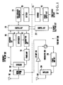
- Fig. 1 is a block diagram illustrating a mobile communication device comprising a removably fitting unit 100 serving as a portable communication device and a fixed unit 200 serving as a power amplifier device into which the portable communication device 100 is removably fitted.
- the configuration of these units 100 and 200 will be briefly described as follows.
- the removably fitting 100 is provided with an antenna 102, an antenna switch 104 coupled to the antenna 102, a duplexer 106 coupled to the antenna switch 104 to switch a signal path, a receiver circuit 108 coupled to the duplexer 106, a control circuit 110 coupled to the receiver circuit 108, a transmitter circuit 112 coupled to the control circuit 110, a synthesizer 114 to control the receiver circuit 108 and the transmitter circuit 112 in accordance with a control signal from the control circuit 110, a power amplifier circuit 116 coupled between the transmitter circuit 112 and the duplexer 106, and a telephone loudspeaker/ microphone 118.
- Reference numeral 120 denotes a battery.
- the fixed unit 200 is provided with an antenna 202, a duplexer 204 coupled to the antenna 202, an RF (radio frequency) amplifier 206 coupled to the duplexer 204, a circulator 208 coupled to the RF amplifier 206 and connectable to the above-mentioned antenna switch 104, and a power amplifier circuit 210 coupled between the circulator 208 and the duplexer 204.
- RF radio frequency
- the fixed unit 200 is further provided with a control circuit 212 capable of effecting a mutual communication with the control circuit 110 provided in the removably fitting unit 100, and an electric charger 214 coupled to a power supply circuit 216 to charge the battery 120 provided in the removably fitting unit 100, when the removably fitting unit 100 is fitted into the fixed unit 200 in order to establish an electrical coupling therebetween.
- Signal flows are indicated by arrow.
- a power supply in the removably fitting unit 100 is switched from the battery 120 to a battery embarked in a vehicle.
- the battery 120 is charged by the charger 214.
- the antenna switch 104 becomes operartive, a signal is received by the vehicle antenna 202 instead of the antenna 102.
- signal transmission is mutually effected between the control circuits 110 and 212.
- Fig. 2 shows a cirucit configuration of the conventional radio communication device Cl, obtained by extracting the parts relevant to the invention from the entire system configuration shown in Fig. 1 for the purpose of facilitating the description.
- the portable communication device 100 comprises an input terminal 1, an amplifier 3 for amplifying an input signal, a power detector circuit 5 connected to the output of the amplifier 3, a differential amplifier 7 responsive to the difference between an output from the power detector circuit 5 and a reference voltage supplied from an input terminal 11 to produce an output signal, and a signal converter circuit 9 responsive to the output signal from the differential circuit 7 to produce a control signal for a control of the amplifier 3.
- the power detector 5 may comprise a directional coupler and a diode.
- Reference numeral 13a denotes an output terminal.
- the power detector circuit 5, the differential amplifier 7 and the signal converter circuit 9 constitutes an automatic output power control circuit.
- the power amplifier device 200 has a circuit configuration similar to that of the portable communication device 100.
- Reference numerals 4, 6, 12, 8 and 10 denote an amplifier, a power detector circuit, a reference voltage input terminal, a differential amplifier and a signal converter circuit, respectively, and reference numerals 13b and 14 denote an input terminal and an output terminal, respectively.
- the power detector circuit 6, the differential amplifier 8 and the signal converter circuit 10 constitutes an automatic output power control circuit.
- Fig. 3 is a perspective view showing the radio communication device C1 comprising the portable communication device 100 and the power amplifier device 200 provided with the circuit connectable with the communication device 100 for amplifying a transmitter output.
- various methods of connecting the portable communication device 100 with the power amplifier device 200 Taking into consideration appearance, convenience in using, volume and shock-proof characteristic etc, it is preferable to connect the device 100 with the device 200 in a manner that most part or the entirety of the communication device 100 is accommodated into the amplifier device 200 as shown in Fig. 3. Accordingly, such a system is ordinarily employed.
- the portable communication device 100 is so designed as to be used in an atomospheric environment. Further, the device 100 requires appearance and weight which impose restrictions on the design of heat dissipation structure. Accordingly, when the accommodating system as shown in Fig. 3 is adopted, ventilation around the portable communication device 100 is liable to be degraded with consequent elevation in temperature, thus considerably impairing heat dissipation effect.
- the device 100 is designed so as to produce the output amounting to several of hundreds of mW to several W, thus producing the same amount of heat in both the usages. For this reason, in the case of using the portable communication device 100 and the power amplifier device 200 connected to each other, the temperature elevation in the portable communication device 100 is far beyond a setting value in the case of sole use of the portable communication device. This results in not only a bad influence on various kinds of circuit characteristics but also likelihood to degrade reliability, thus producing a serious problem in the radio communication device.
- An object of the present invention is to provide a radio communication device which can solve a problem of excessive heat generation in the communication device when a portable communication device is accommodated into a power amplifier device in a manner stated above.
- a radio communication device comprising; first device means provided with a radio transmitter and receiver circuit; second device means adapted to be electrically coupled to the first device means and for amplifying a transmitter output power level therefrom; and detector means for detecting that an electrical coupling between the first and second device means is established, thereby effecting a control such that the transmitter output power level is suppressed to a minimum input level required for the second device means.
- the detector means may comprise a detector circuit operative to produce information indicative of the establishment of the electrical coupling between the first and second device means.
- the first device means may be configured as a radio communication circuit comprising a power amplifier, and an automatic output power control circuit coupled to the power amplifier to control the power amplifier depending upon an output level of the power amplifier, the detector circuit being coupled to the automatic output power control circuit, whereby the automatic output power control circuit becomes operative to vary the output level of the power amplifier in accordance with the information from the detector circuit.
- the automatic output power control circuit may comprise an output power detector coupled to the power amplifier, a differential amplifier responsive to a difference between the output level of the power detector and a reference voltage, and a control signal converter for converting an output from the differential amplifier into a control signal for controlling the power amplifier.
- the automatic output power control circuit further comprises a reference voltage producing circuit for producing the reference voltage.
- the detector circuit may be configured as a circuit for voltage-dividing the reference voltage from the reference voltage producing circuit.
- the first device means may be adapted to be removably fitted into the second device means.
- the detector means may include a variable resistor and a switch responsive to the establishment of an electrical connection between the portable communication means and the amplifier means.
- the detector means may be provided, at the first device means, with a switch element, a contact provided at the switch element, a movable pin, and a first connector, and at the second device means with a projection and a second connector, whereby when the first device means is fitted into the second device means, the projection pushes the pin to turn on the switch element.
- the first and second device means are provided with control circuit which can be mutually communicated with each other, whereby when the control unit is operative to deliver a power-down signal to the reference voltage producing circuit in response to information indicative of establishment of the electrical connection between the first and second device means to turn on a switch element, a control is effected such that an output level of the power amplifier is suppressed to a minimum input level required for the power amplifier means.
- a method of controlling a transmitter output power level of a radio communication device comprising portable radio communication means provided with a radio transmitter and receiver circuit and power amplifier means adapted to be electrically coupled to the radio communication means and for amplifying a transmitter output therefrom, characterized in that the method comprises the steps of detecting that an electrical coupling between the portable communication means and the power amplifier means is established, and effecting a control such that the transmitter output level is kept at a minimum level required for the power amplifier means.
- Fig. 4 is a circuit diagram illustrating the embodiment of the invention.
- the portable communication device 100 and the amplifier device 200 are provided with the power amplifier and the automatic output power control circuit, in an independent manner, respectively. For this reason, in the case of using the portable communication device 100 with it being connected to the power amplifier device 200, the power amplifier 3 provided in the portable communication device 100 dissipates the same amount of power as that when solely the portable communication device 100 is used. This brings about a problem in heat dissipation as previously mentioned.
- the portable communication device 100 is further provided with a circuit for adjusting a reference voltage comprising a circuit 15 operative to produce a controllable reference voltage V f and a detector circuit 16 for detecting that an electrical connection or coupling between the communication device 100 and the amplifier device 200 is established.
- the detector circuit 16 becomes operative to convert information K indicating that the power amplifier device 200 is connected to the communication device 100 into an electric signal S which in turn is delivered to the controllable reference voltage producing circuit 15.
- the circuit 15 becomes operative to produce a reference voltage V f in response to the electric signal S.
- the power amplifier 3 is controlled so that its output power is lowered in accordance with an output from the differential amplifier 7 which amplifies the difference between the modified reference voltage V f and a dc signal S1 from the output power detector circuit 5.
- an output power level P of the portable communication device 100 when the power amplifier 4 has a sufficiently large gain, it is possible to use a relatively small value as power level applied to the input terminal 13b, i.e., an output power level P of the portable communication device 100.
- the power amplifier 4 has a gain of 30 dB and the power amplifier device 200 is required to produce an output power level of 10 W from the output terminal 14, it is required to input a power level of 10 mW to the input terminal 13.
- the power amplifier 3 provided in the portable communication device 100 has ability to produce an output of several of hundreds of mW to several W to ensure that the portable communication device 100 can be used alone. For this reason, a measure for lowering an output power level P of the portable communication device 100 is required.
- the overall gain of the radio communication device C2 of the invention is equal to that of the conventional radio communication device Cl shown in Fig. 2.
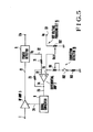
- Fig. 5 is a detailed circuit diagram illustrating an embodiment according to the present invention wherein circuit components identical to those shown in Fig. 4 are designated by the same reference numerals, respectively.
- An input signal to the input terminal 1 is amplified by the power amplifier 3.
- the signal thus amplified is delivered to the power detector circuit 5 through a line 21.
- the signal passed through the power detector circuit 5 is outputted from the output terminal 13a.
- the output signal Vp detected by the detector circuit 5 is applied to a resistor 71 through a line 22 and then is inputted to an inverting input terminal 72 of the differential amplifier 7.
- a feedback resistor 73 is connected between an output terminal 74 and the inverting input terminal 72 to form a feedfack loop.
- the differenctial amplifier 7 provided with the feedback resistor may be constituted by a comparison circuit.
- a power supply voltage Vs is applied to a power supply voltage terminal 151.
- a variable resistor 152 to which the power supply voltage Vs is applied constitutes the circuit 15 which is operative to produce a desired reference voltage by adjusting the value of the variable resistor 152.
- the reference voltage VR EF thus produced is inputted to a non-inverting input terminal 75 of the differential amplifier 7.
- the differential amplifier 7 becomes operative to compare the output signal inputted to the inverting input terminal 72 with the reference voltage V REF inputted to the non-inverting input terminal 75 to amplify the difference therebetween, thus producing a control signal on the output terminal 74.
- the control signal is inputted to the control signal converter circuit 9 through a line 23.
- the control signal converter circuit 9 becomes operative to convert the control signal into a voltage suitable for control of the power amplifier 3.
- the voltage thus obtained is applied to the power amplifier 3 through a line 24.
- This control voltage is proportional to the difference between the reference voltage V REF and the output signal. Accordingly, the output power of the communication device varies inversely proportional to the control voltage. This provides an effect for allowing the output power to return to its initial value. Namely, the output power is kept constant by varying the control voltage so that the output voltage and the reference voltage V REF are equal to each other.
- the detector circuit 16 comprises a variable resistor 161, a switch 162 and a resistor 163 which are connected in series between the non-inverting input terminal 75 of the differential amplifier 7 and ground.
- the switch 162 is cut off. Accordingly, the resistors 161 and 163 do not serve as a voltage divider.
- the switch 162 turns on. As a result, the non-inverting input terminal 75 of the differential amplifier 7 is also connected to ground through the resistors 161 and 163.
- the setting of the reference voltage V REF can be effected not only by the variable resistor 152 but also by the variable resistor 161 and the resistor 163. It is now assumed that the resistance value of the variable resistor 152 between its slider and one end close to ground is R 152 ' and its maximum resistance value is R 152 and the resistance values of the resistors 161 and 163 are R 161 ' and R 163' respectively.
- the reference voltage is expressed as follows.
- the switch 162 when the switch 162 is turned on, the reference voltage V REF ' becomes smaller than that when the switch 162 is cut off. As a result, the output power of the removably fitting unit is reduced.
- Fig. 6 is a cross sectional view illustrating the connection detector switch 162.
- the switch 162 is provided on the side of the removably fitting unit 100 with a casing 121, a switch element 122, an electrical contact 123, a lever 124, a pin 125, and a connector 126 and on the side of the fixed unit 200, casing 221, a projection 222 and a connector 223.
- the pin 125 is moved upwards by the projection 222 to bring the lever 124 into contact with the contact 123 to thereby turn on the switch element 122.
- the switch operation is mechanically determined depending upon whether the removably fitting unit 100 and the fixed unit 200 are connected with each other or not.
- the embodiment shown in Fig. 6 can be modified as follows.
- the control circuits 110 and 212 (Fig. 1) via the connectors 126 and 223 (Fig. 6).
- the switch 162 (Fig. 5) is turned on, thus effecting a control such that an output power level of the unit 100 is suitably suppressed.
- the present invention can provide a system of varying a reference voltage from the reference voltage producing circuit 15 in accordance with an output from the detector circuit 16 for detecting that the connection of the portable communication device 100 and the power amplifier device 200 is established, thus controlling transmitter power from the power amplifier 3 provided in the portable communication device 100.
- This system makes it possible to suppress an excessive heat generation in the communication device which is problematic when the portable communication device is used by being accommodated into the power amplifier device.
- a control is effected in a manner to vary a reference voltage V f of the automatic output power control circuit provided in the communication device to a minimum input required for the power amplifier device 200, thus suppressing heat generation in the communication device.
Abstract
Description
- The present invention relates to a radio communication system, and more particularly to a radio communication device comprising a portable communication device and a power amplifier device connectable to the portable communication device to amplify a transmitter output therefrom. Specifically, the present invention is concerned with a method of effecting a control such that transmitter output power level of the portable communication device is kept at a minimum level required for the power amplifier device.
- In general, portable or handy type radio communication devices have restrictions in respect to a battery capacity and a heat dissipation structure. Accordingly, their transmitter output is limited to about several of hundreds of mW (milliwatt) to about several watts. Such a transmitter output is of a small value as compared to that of a radio communication device carried on a vehicle or a fixed radio communication device. In other words, in case where a larger transmitter output is needed, it is necessary to provide an amplifier device connectable to the portable communication device for amplifying its transmitter output.
- The configuration of a conventional communication device designed in consideration of the above and its problems will be described in connection with the case where the communication device is applied to a mobile communication system e.g. a vehicle telephone communication.
- Fig. 1 is a block diagram illustrating a mobile communication device comprising a removably
fitting unit 100 serving as a portable communication device and a fixedunit 200 serving as a power amplifier device into which theportable communication device 100 is removably fitted. The configuration of theseunits antenna 102, anantenna switch 104 coupled to theantenna 102, aduplexer 106 coupled to theantenna switch 104 to switch a signal path, areceiver circuit 108 coupled to theduplexer 106, acontrol circuit 110 coupled to thereceiver circuit 108, atransmitter circuit 112 coupled to thecontrol circuit 110, asynthesizer 114 to control thereceiver circuit 108 and thetransmitter circuit 112 in accordance with a control signal from thecontrol circuit 110, apower amplifier circuit 116 coupled between thetransmitter circuit 112 and theduplexer 106, and a telephone loudspeaker/microphone 118.Reference numeral 120 denotes a battery. Thefixed unit 200 is provided with anantenna 202, aduplexer 204 coupled to theantenna 202, an RF (radio frequency)amplifier 206 coupled to theduplexer 204, acirculator 208 coupled to theRF amplifier 206 and connectable to the above-mentionedantenna switch 104, and apower amplifier circuit 210 coupled between thecirculator 208 and theduplexer 204. Thefixed unit 200 is further provided with acontrol circuit 212 capable of effecting a mutual communication with thecontrol circuit 110 provided in the removablyfitting unit 100, and anelectric charger 214 coupled to apower supply circuit 216 to charge thebattery 120 provided in the removablyfitting unit 100, when the removablyfitting unit 100 is fitted into thefixed unit 200 in order to establish an electrical coupling therebetween. Signal flows are indicated by arrow. - When the removably fitting
unit 100 is connected with thefixed unit 200, a power supply in the removablyfitting unit 100 is switched from thebattery 120 to a battery embarked in a vehicle. As a result, thebattery 120 is charged by thecharger 214. At this time, since theantenna switch 104 becomes operartive, a signal is received by thevehicle antenna 202 instead of theantenna 102. Upon establishment of an eletrical connection between the removably fittingunit 100 and thefixed unit 200, signal transmission is mutually effected between thecontrol circuits - Fig. 2 shows a cirucit configuration of the conventional radio communication device Cl, obtained by extracting the parts relevant to the invention from the entire system configuration shown in Fig. 1 for the purpose of facilitating the description.
- As shown in this figure, the
portable communication device 100 comprises an input terminal 1, anamplifier 3 for amplifying an input signal, apower detector circuit 5 connected to the output of theamplifier 3, adifferential amplifier 7 responsive to the difference between an output from thepower detector circuit 5 and a reference voltage supplied from aninput terminal 11 to produce an output signal, and asignal converter circuit 9 responsive to the output signal from thedifferential circuit 7 to produce a control signal for a control of theamplifier 3. Thepower detector 5 may comprise a directional coupler and a diode.Reference numeral 13a denotes an output terminal. Thepower detector circuit 5, thedifferential amplifier 7 and thesignal converter circuit 9 constitutes an automatic output power control circuit. Thepower amplifier device 200 has a circuit configuration similar to that of theportable communication device 100.Reference numerals reference numerals power detector circuit 6, thedifferential amplifier 8 and thesignal converter circuit 10 constitutes an automatic output power control circuit. - An explanation will be made in connection with a serious problem occurring in designing heat dissipation structure of the portable radio communication device when the conventional radio communication configured as shown in Fig. 2 is used.
- Fig. 3 is a perspective view showing the radio communication device C1 comprising the
portable communication device 100 and thepower amplifier device 200 provided with the circuit connectable with thecommunication device 100 for amplifying a transmitter output. In addition to the connecting system shown in Fig. 3, there are proposed various methods of connecting theportable communication device 100 with thepower amplifier device 200. Taking into consideration appearance, convenience in using, volume and shock-proof characteristic etc, it is preferable to connect thedevice 100 with thedevice 200 in a manner that most part or the entirety of thecommunication device 100 is accommodated into theamplifier device 200 as shown in Fig. 3. Accordingly, such a system is ordinarily employed. - Primarily, the
portable communication device 100 is so designed as to be used in an atomospheric environment. Further, thedevice 100 requires appearance and weight which impose restrictions on the design of heat dissipation structure. Accordingly, when the accommodating system as shown in Fig. 3 is adopted, ventilation around theportable communication device 100 is liable to be degraded with consequent elevation in temperature, thus considerably impairing heat dissipation effect. - To be more specific, in the radio communication device Cl based on the connecting system as shown in Fig. 3, irrespective of the fact that the
portable communication device 100 is solely used or it is combined with thepower amplifier device 200, thedevice 100 is designed so as to produce the output amounting to several of hundreds of mW to several W, thus producing the same amount of heat in both the usages. For this reason, in the case of using theportable communication device 100 and thepower amplifier device 200 connected to each other, the temperature elevation in theportable communication device 100 is far beyond a setting value in the case of sole use of the portable communication device. This results in not only a bad influence on various kinds of circuit characteristics but also likelihood to degrade reliability, thus producing a serious problem in the radio communication device. - An object of the present invention is to provide a radio communication device which can solve a problem of excessive heat generation in the communication device when a portable communication device is accommodated into a power amplifier device in a manner stated above.
- According to the present invention, there is provided a radio communication device comprising; first device means provided with a radio transmitter and receiver circuit; second device means adapted to be electrically coupled to the first device means and for amplifying a transmitter output power level therefrom; and detector means for detecting that an electrical coupling between the first and second device means is established, thereby effecting a control such that the transmitter output power level is suppressed to a minimum input level required for the second device means. The detector means may comprise a detector circuit operative to produce information indicative of the establishment of the electrical coupling between the first and second device means.
- The first device means may be configured as a radio communication circuit comprising a power amplifier, and an automatic output power control circuit coupled to the power amplifier to control the power amplifier depending upon an output level of the power amplifier, the detector circuit being coupled to the automatic output power control circuit, whereby the automatic output power control circuit becomes operative to vary the output level of the power amplifier in accordance with the information from the detector circuit.
- The automatic output power control circuit may comprise an output power detector coupled to the power amplifier, a differential amplifier responsive to a difference between the output level of the power detector and a reference voltage, and a control signal converter for converting an output from the differential amplifier into a control signal for controlling the power amplifier.
- The automatic output power control circuit further comprises a reference voltage producing circuit for producing the reference voltage.
- The detector circuit may be configured as a circuit for voltage-dividing the reference voltage from the reference voltage producing circuit.
- The first device means may be adapted to be removably fitted into the second device means.
- The detector means may include a variable resistor and a switch responsive to the establishment of an electrical connection between the portable communication means and the amplifier means.
- The detector means may be provided, at the first device means, with a switch element, a contact provided at the switch element, a movable pin, and a first connector, and at the second device means with a projection and a second connector, whereby when the first device means is fitted into the second device means, the projection pushes the pin to turn on the switch element.
- The first and second device means are provided with control circuit which can be mutually communicated with each other, whereby when the control unit is operative to deliver a power-down signal to the reference voltage producing circuit in response to information indicative of establishment of the electrical connection between the first and second device means to turn on a switch element, a control is effected such that an output level of the power amplifier is suppressed to a minimum input level required for the power amplifier means.
- According to the present invention, there is also provided a method of controlling a transmitter output power level of a radio communication device comprising portable radio communication means provided with a radio transmitter and receiver circuit and power amplifier means adapted to be electrically coupled to the radio communication means and for amplifying a transmitter output therefrom, characterized in that the method comprises the steps of detecting that an electrical coupling between the portable communication means and the power amplifier means is established, and effecting a control such that the transmitter output level is kept at a minimum level required for the power amplifier means.
- The features and advantages of a radio communication device according to the present invention will become more apparent from the following description taken in conjunction with the accompanying drawings, in which:
- Fig. 1 is a block diagram illustrating a mobile communication system to which the present invention is applied;
- Fig. 2 is a circuit diagram illustrating a conventional radio communication device;
- Fig. 3 is a perspective view showing a connecting system for accommodating a portable communication device into a power amplifier device in the device shown in Fig. 2;
- Fig. 4 is a circuit diagram illustrating an embodiment of a radio communication device according to the present invention;
- Fig. 5 is a circuit diagram showing details of Fig. 4; and
- Fig. 6 is a cross sectional view illustrating an example of a connection detector switch employed in the present invention.
- A preferred embodiment of radio transmitter according to the present invention will be described with reference to attached drawings. Fig. 4 is a circuit diagram illustrating the embodiment of the invention.
- As understood from Fig. 2, the
portable communication device 100 and theamplifier device 200 are provided with the power amplifier and the automatic output power control circuit, in an independent manner, respectively. For this reason, in the case of using theportable communication device 100 with it being connected to thepower amplifier device 200, thepower amplifier 3 provided in theportable communication device 100 dissipates the same amount of power as that when solely theportable communication device 100 is used. This brings about a problem in heat dissipation as previously mentioned. - In contrast, in the preferred embodiment shown in Fig. 4, the
portable communication device 100 is further provided with a circuit for adjusting a reference voltage comprising acircuit 15 operative to produce a controllable reference voltage Vf and adetector circuit 16 for detecting that an electrical connection or coupling between thecommunication device 100 and theamplifier device 200 is established. - Accordingly, when the
communication device 100 is connected to thepower amplifier device 200, thedetector circuit 16 becomes operative to convert information K indicating that thepower amplifier device 200 is connected to thecommunication device 100 into an electric signal S which in turn is delivered to the controllable referencevoltage producing circuit 15. Thecircuit 15 becomes operative to produce a reference voltage Vf in response to the electric signal S. Thus, thepower amplifier 3 is controlled so that its output power is lowered in accordance with an output from thedifferential amplifier 7 which amplifies the difference between the modified reference voltage Vf and a dc signal S1 from the outputpower detector circuit 5. - In this instance, when the
power amplifier 4 has a sufficiently large gain, it is possible to use a relatively small value as power level applied to theinput terminal 13b, i.e., an output power level P of theportable communication device 100. For instance, where thepower amplifier 4 has a gain of 30 dB and thepower amplifier device 200 is required to produce an output power level of 10 W from theoutput terminal 14, it is required to input a power level of 10 mW to the input terminal 13. Thepower amplifier 3 provided in theportable communication device 100 has ability to produce an output of several of hundreds of mW to several W to ensure that theportable communication device 100 can be used alone. For this reason, a measure for lowering an output power level P of theportable communication device 100 is required. In the above-mentioned discussion, it is assumed that there is no problem of heat dissipation in thepower amplifier device 200, and the overall gain of the radio communication device C2 of the invention is equal to that of the conventional radio communication device Cl shown in Fig. 2. - Fig. 5 is a detailed circuit diagram illustrating an embodiment according to the present invention wherein circuit components identical to those shown in Fig. 4 are designated by the same reference numerals, respectively. An input signal to the input terminal 1 is amplified by the
power amplifier 3. The signal thus amplified is delivered to thepower detector circuit 5 through aline 21. The signal passed through thepower detector circuit 5 is outputted from theoutput terminal 13a. The output signal Vp detected by thedetector circuit 5 is applied to a resistor 71 through aline 22 and then is inputted to an invertinginput terminal 72 of thedifferential amplifier 7. Afeedback resistor 73 is connected between anoutput terminal 74 and the invertinginput terminal 72 to form a feedfack loop. Thedifferenctial amplifier 7 provided with the feedback resistor may be constituted by a comparison circuit. A power supply voltage Vs is applied to a powersupply voltage terminal 151. Avariable resistor 152 to which the power supply voltage Vs is applied constitutes thecircuit 15 which is operative to produce a desired reference voltage by adjusting the value of thevariable resistor 152. The reference voltage VREF thus produced is inputted to anon-inverting input terminal 75 of thedifferential amplifier 7. Thedifferential amplifier 7 becomes operative to compare the output signal inputted to the invertinginput terminal 72 with the reference voltage VREF inputted to thenon-inverting input terminal 75 to amplify the difference therebetween, thus producing a control signal on theoutput terminal 74. The control signal is inputted to the controlsignal converter circuit 9 through aline 23. The controlsignal converter circuit 9 becomes operative to convert the control signal into a voltage suitable for control of thepower amplifier 3. The voltage thus obtained is applied to thepower amplifier 3 through aline 24. This control voltage is proportional to the difference between the reference voltage VREF and the output signal. Accordingly, the output power of the communication device varies inversely proportional to the control voltage. This provides an effect for allowing the output power to return to its initial value. Namely, the output power is kept constant by varying the control voltage so that the output voltage and the reference voltage VREF are equal to each other. - Further, as shown in Fig. 5, the
detector circuit 16 comprises avariable resistor 161, aswitch 162 and aresistor 163 which are connected in series between thenon-inverting input terminal 75 of thedifferential amplifier 7 and ground. When the removably fitting unit (portable communication device) 100 is solely used, theswitch 162 is cut off. Accordingly, theresistors fitting unit 100 and the fixedunit 200 are connected to each other, theswitch 162 turns on. As a result, thenon-inverting input terminal 75 of thedifferential amplifier 7 is also connected to ground through theresistors variable resistor 152 but also by thevariable resistor 161 and theresistor 163. It is now assumed that the resistance value of thevariable resistor 152 between its slider and one end close to ground is R152' and its maximum resistance value is R152 and the resistance values of theresistors - When the
switch 162 is turned off, the reference voltage is expressed as follows.
- When the
switch 162 is turned on, the reference voltage is expressed as follows.


- Accordingly, when the
switch 162 is turned on, the reference voltage VREF' becomes smaller than that when theswitch 162 is cut off. As a result, the output power of the removably fitting unit is reduced. - Fig. 6 is a cross sectional view illustrating the
connection detector switch 162. Theswitch 162 is provided on the side of the removablyfitting unit 100 with acasing 121, a switch element 122, anelectrical contact 123, a lever 124, a pin 125, and aconnector 126 and on the side of the fixedunit 200, casing 221, aprojection 222 and aconnector 223. When the removablyfitting unit 100 is connected to the fixedunit 200, the pin 125 is moved upwards by theprojection 222 to bring the lever 124 into contact with thecontact 123 to thereby turn on the switch element 122. On the contrary, when the removablyfitting unit 100 is removed or separated from the fixedunit 200, the pin 125 moves downwards so that the lever 124 is released from thecontact 123, thus turning off the switch element 122. The bothconnectors fitting unit 100 and the fixedunit 200 are connected to each other. - In the above-mentioned detector circuit shown in Fig. 6, the switch operation is mechanically determined depending upon whether the removably
fitting unit 100 and the fixedunit 200 are connected with each other or not. In addition, the embodiment shown in Fig. 6 can be modified as follows. When the bothunits control circuits 110 and 212 (Fig. 1) via theconnectors 126 and 223 (Fig. 6). Accordingly, by allowing thecontrol circuit 212 provided in the fixedunit 200 to deliver a power down signal to the referencevoltage producing circuit 15 provided in the removablyfitting unit 100 when thecontrol circuit 212 receives a signal indicating that an electrical connection between both the units is established, the switch 162 (Fig. 5) is turned on, thus effecting a control such that an output power level of theunit 100 is suitably suppressed. - As described above, the present invention can provide a system of varying a reference voltage from the reference
voltage producing circuit 15 in accordance with an output from thedetector circuit 16 for detecting that the connection of theportable communication device 100 and thepower amplifier device 200 is established, thus controlling transmitter power from thepower amplifier 3 provided in theportable communication device 100. This system makes it possible to suppress an excessive heat generation in the communication device which is problematic when the portable communication device is used by being accommodated into the power amplifier device. - In other words, in accordance with this system, when the
portable communication device 100 has been connected to thepower amplifier device 200, a control is effected in a manner to vary a reference voltage Vf of the automatic output power control circuit provided in the communication device to a minimum input required for thepower amplifier device 200, thus suppressing heat generation in the communication device.
Claims (12)
Applications Claiming Priority (2)
| Application Number | Priority Date | Filing Date | Title |
|---|---|---|---|
| JP78967/84 | 1984-04-19 | ||
| JP59078967A JPS60223231A (en) | 1984-04-19 | 1984-04-19 | Radio communication equipment |
Publications (3)
| Publication Number | Publication Date |
|---|---|
| EP0159670A2 true EP0159670A2 (en) | 1985-10-30 |
| EP0159670A3 EP0159670A3 (en) | 1986-10-08 |
| EP0159670B1 EP0159670B1 (en) | 1989-04-12 |
Family
ID=13676670
Family Applications (1)
| Application Number | Title | Priority Date | Filing Date |
|---|---|---|---|
| EP85104714A Expired EP0159670B1 (en) | 1984-04-19 | 1985-04-18 | Radio communication device and method of controlling transmitter output power |
Country Status (5)
| Country | Link |
|---|---|
| US (1) | US4654882A (en) |
| EP (1) | EP0159670B1 (en) |
| JP (1) | JPS60223231A (en) |
| CA (1) | CA1230926A (en) |
| DE (1) | DE3569443D1 (en) |
Cited By (11)
| Publication number | Priority date | Publication date | Assignee | Title |
|---|---|---|---|---|
| EP0248033A4 (en) * | 1985-11-01 | 1987-11-02 | Motorola Inc | Multi-level power amplifying circuitry for portable radio transceivers. |
| EP0331435A2 (en) * | 1988-02-29 | 1989-09-06 | Kabushiki Kaisha Toshiba | Radio telephone apparatus |
| EP0336375A1 (en) * | 1988-04-08 | 1989-10-11 | Siemens Aktiengesellschaft | Transmitting apparatus |
| EP0392132A2 (en) * | 1989-04-10 | 1990-10-17 | Mitsubishi Denki Kabushiki Kaisha | Radio transceiver apparatus with booster |
| EP0413355A2 (en) * | 1989-08-18 | 1991-02-20 | Nec Corporation | Vehicular power booster circuitry for multi-level portable transceiver |
| AU610999B2 (en) * | 1988-06-15 | 1991-05-30 | Mitsubishi Denki Kabushiki Kaisha | Transmission power control circuit and method |
| EP0452011A2 (en) * | 1990-03-29 | 1991-10-16 | Nokia Mobile Phones Ltd. | Hand-held transceiver as a modular unit |
| AU631421B2 (en) * | 1989-04-24 | 1992-11-26 | Telenokia Oy | High-frequency amplifier of a radio transmitter |
| US5203020A (en) * | 1988-06-14 | 1993-04-13 | Kabushiki Kaisha Toshiba | Method and apparatus for reducing power consumption in a radio telecommunication apparatus |
| EP0654898A2 (en) * | 1993-11-19 | 1995-05-24 | Matsushita Communication Industrial Co., Ltd. | Transmission circuit |
| GB2313263A (en) * | 1996-05-16 | 1997-11-19 | Motorola Inc | Circuit for adjusting transmit power in a radiotelephone |
Families Citing this family (46)
| Publication number | Priority date | Publication date | Assignee | Title |
|---|---|---|---|---|
| JPH0644716B2 (en) * | 1984-08-14 | 1994-06-08 | 日本電気株式会社 | Wireless communication device |
| JPS63226124A (en) * | 1986-10-29 | 1988-09-20 | Oki Electric Ind Co Ltd | Level control circuit for radio equipment |
| JPH0432860Y2 (en) * | 1987-07-20 | 1992-08-06 | ||
| JPH0432859Y2 (en) * | 1987-07-20 | 1992-08-06 | ||
| JPS6452322U (en) * | 1987-09-26 | 1989-03-31 | ||
| US4875038A (en) * | 1988-01-07 | 1989-10-17 | Motorola, Inc. | Frequency division multiplexed acknowledge back paging system |
| US4882579A (en) * | 1988-01-07 | 1989-11-21 | Motorola, Inc. | Code division multiplexed acknowledge back paging system |
| US4825193A (en) * | 1988-01-07 | 1989-04-25 | Motorola, Inc. | Acknowledge back pager with adaptive variable transmitter output power |
| US4823123A (en) * | 1988-01-07 | 1989-04-18 | Motorola, Inc. | Knowledge back pager with frequency control apparatus |
| US4891637A (en) * | 1988-01-07 | 1990-01-02 | Motorola, Inc. | Acknowledge back pager with apparatus for controlling transmit frequency |
| JPH0278331A (en) * | 1988-09-14 | 1990-03-19 | Nec Corp | Transmitter-receiver for mobile communication |
| JPH02246531A (en) * | 1989-03-20 | 1990-10-02 | Fujitsu Ltd | Transmission interruption detecting circuit for variable transmission power type transmitter |
| US4989260A (en) * | 1989-05-17 | 1991-01-29 | The Quaker Oats Company | Transmitter with power reduction to compensate for varying radiated electric field strength when switching between batteries and AC power |
| US5142279A (en) * | 1989-06-05 | 1992-08-25 | Motorola, Inc. | Acknowledge back paging system having the capability of matching variable length data messages to pager addresses |
| JP2746685B2 (en) * | 1989-09-06 | 1998-05-06 | 富士通株式会社 | Transmission output control circuit |
| SE466722B (en) * | 1990-07-31 | 1992-03-23 | Ericsson Telefon Ab L M | DRIVEN DRIVING A MOBILE PHONE |
| JP2568779B2 (en) | 1991-12-10 | 1997-01-08 | 松下電器産業株式会社 | Mobile phone equipment |
| US5457814A (en) * | 1993-10-02 | 1995-10-10 | Nokia Mobile Phones Ltd. | Power boost system for cellular telephone |
| AU667140B2 (en) * | 1992-11-26 | 1996-03-07 | Nec Corporation | Booster for use in combination with radio apparatus |
| KR950007973B1 (en) * | 1992-11-27 | 1995-07-21 | 삼성전자주식회사 | The high-frequency output-level compensating circuit of mobile phone |
| JPH06265430A (en) * | 1993-03-11 | 1994-09-22 | Nissan Motor Co Ltd | Cylinder inner pressure sensor |
| JPH06276146A (en) * | 1993-03-19 | 1994-09-30 | Fujitsu Ltd | Traveling telephone system |
| JPH08501197A (en) * | 1993-03-26 | 1996-02-06 | クァルコム・インコーポレーテッド | Power amplifier bias control circuit and method |
| DE4316526B4 (en) * | 1993-05-18 | 2005-11-10 | Philips Intellectual Property & Standards Gmbh | Transmitter with a controllable power amplifier |
| JPH06334541A (en) * | 1993-05-25 | 1994-12-02 | Sony Corp | Radio transmitter |
| US5339046A (en) * | 1993-06-03 | 1994-08-16 | Alps Electric Co., Ltd. | Temperature compensated variable gain amplifier |
| US5732335A (en) * | 1995-04-28 | 1998-03-24 | Telefonaktiebolaget Lm Ericsson | Externally controlled output power by means of antenna keying |
| US5872481A (en) * | 1995-12-27 | 1999-02-16 | Qualcomm Incorporated | Efficient parallel-stage power amplifier |
| US5974041A (en) * | 1995-12-27 | 1999-10-26 | Qualcomm Incorporated | Efficient parallel-stage power amplifier |
| US6230031B1 (en) * | 1997-03-31 | 2001-05-08 | Oki Telecom, Inc. | Power amplifying circuitry for wireless radio transceivers |
| US6069525A (en) * | 1997-04-17 | 2000-05-30 | Qualcomm Incorporated | Dual-mode amplifier with high efficiency and high linearity |
| US6038457A (en) * | 1997-12-05 | 2000-03-14 | Motorola, Inc. | Apparatus and method for detecting and powering an accessory |
| USD419160S (en) * | 1998-05-14 | 2000-01-18 | Northrop Grumman Corporation | Personal communications unit docking station |
| USD421002S (en) * | 1998-05-15 | 2000-02-22 | Northrop Grumman Corporation | Personal communications unit handset |
| US6141426A (en) * | 1998-05-15 | 2000-10-31 | Northrop Grumman Corporation | Voice operated switch for use in high noise environments |
| US6169730B1 (en) | 1998-05-15 | 2001-01-02 | Northrop Grumman Corporation | Wireless communications protocol |
| US6223062B1 (en) | 1998-05-15 | 2001-04-24 | Northrop Grumann Corporation | Communications interface adapter |
| US6243573B1 (en) | 1998-05-15 | 2001-06-05 | Northrop Grumman Corporation | Personal communications system |
| US6041243A (en) * | 1998-05-15 | 2000-03-21 | Northrop Grumman Corporation | Personal communications unit |
| US6304559B1 (en) | 1998-05-15 | 2001-10-16 | Northrop Grumman Corporation | Wireless communications protocol |
| US6069526A (en) * | 1998-08-04 | 2000-05-30 | Qualcomm Incorporated | Partial or complete amplifier bypass |
| JP2003133972A (en) * | 2001-10-29 | 2003-05-09 | Fujitsu Ltd | Electronic device having wireless transmitter |
| DE10218828A1 (en) * | 2002-04-26 | 2003-11-06 | Siemens Ag | Mobile RF device with transmission power limitation, can be set to maximum transmission power via mobilephone menu with user personally selecting maximum acceptable radiative loading level |
| US8536950B2 (en) * | 2009-08-03 | 2013-09-17 | Qualcomm Incorporated | Multi-stage impedance matching |
| US8102205B2 (en) | 2009-08-04 | 2012-01-24 | Qualcomm, Incorporated | Amplifier module with multiple operating modes |
| JP2015050548A (en) * | 2013-08-30 | 2015-03-16 | 株式会社タムラ製作所 | Transmitter and radio communications system using the same |
Citations (2)
| Publication number | Priority date | Publication date | Assignee | Title |
|---|---|---|---|---|
| US4189676A (en) * | 1978-04-13 | 1980-02-19 | Motorola, Inc. | Switching system utilizing flexible circuit with transmission line for matched impedance connections |
| US4353037A (en) * | 1980-08-11 | 1982-10-05 | Motorola, Inc. | Amplifier protection circuit |
Family Cites Families (4)
| Publication number | Priority date | Publication date | Assignee | Title |
|---|---|---|---|---|
| US4095184A (en) * | 1976-11-01 | 1978-06-13 | Hochstein Peter A | Radio transceiver power booster |
| JPS5694848A (en) * | 1979-12-28 | 1981-07-31 | Nec Corp | Control system of transmitter |
| JPS6110327Y2 (en) * | 1980-01-10 | 1986-04-03 | ||
| JPS6041821A (en) * | 1983-08-18 | 1985-03-05 | Nec Corp | Transmission output power controller |
-
1984
- 1984-04-19 JP JP59078967A patent/JPS60223231A/en active Granted
-
1985
- 1985-04-15 US US06/723,633 patent/US4654882A/en not_active Expired - Lifetime
- 1985-04-16 CA CA000479261A patent/CA1230926A/en not_active Expired
- 1985-04-18 DE DE8585104714T patent/DE3569443D1/en not_active Expired
- 1985-04-18 EP EP85104714A patent/EP0159670B1/en not_active Expired
Patent Citations (2)
| Publication number | Priority date | Publication date | Assignee | Title |
|---|---|---|---|---|
| US4189676A (en) * | 1978-04-13 | 1980-02-19 | Motorola, Inc. | Switching system utilizing flexible circuit with transmission line for matched impedance connections |
| US4353037A (en) * | 1980-08-11 | 1982-10-05 | Motorola, Inc. | Amplifier protection circuit |
Cited By (20)
| Publication number | Priority date | Publication date | Assignee | Title |
|---|---|---|---|---|
| EP0248033A1 (en) * | 1985-11-01 | 1987-12-09 | Motorola Inc | Multi-level power amplifying circuitry for portable radio transceivers. |
| EP0248033A4 (en) * | 1985-11-01 | 1987-11-02 | Motorola Inc | Multi-level power amplifying circuitry for portable radio transceivers. |
| EP0331435A2 (en) * | 1988-02-29 | 1989-09-06 | Kabushiki Kaisha Toshiba | Radio telephone apparatus |
| EP0331435A3 (en) * | 1988-02-29 | 1991-07-31 | Kabushiki Kaisha Toshiba | Radio telephone apparatus |
| EP0336375A1 (en) * | 1988-04-08 | 1989-10-11 | Siemens Aktiengesellschaft | Transmitting apparatus |
| US5203020A (en) * | 1988-06-14 | 1993-04-13 | Kabushiki Kaisha Toshiba | Method and apparatus for reducing power consumption in a radio telecommunication apparatus |
| AU610999B2 (en) * | 1988-06-15 | 1991-05-30 | Mitsubishi Denki Kabushiki Kaisha | Transmission power control circuit and method |
| EP0392132A2 (en) * | 1989-04-10 | 1990-10-17 | Mitsubishi Denki Kabushiki Kaisha | Radio transceiver apparatus with booster |
| AU612920B2 (en) * | 1989-04-10 | 1991-07-18 | Mitsubishi Denki Kabushiki Kaisha | Radio transceiver apparatus with booster |
| EP0392132A3 (en) * | 1989-04-10 | 1992-05-06 | Mitsubishi Denki Kabushiki Kaisha | Radio transceiver apparatus with booster |
| AU631421B2 (en) * | 1989-04-24 | 1992-11-26 | Telenokia Oy | High-frequency amplifier of a radio transmitter |
| EP0413355A2 (en) * | 1989-08-18 | 1991-02-20 | Nec Corporation | Vehicular power booster circuitry for multi-level portable transceiver |
| EP0413355A3 (en) * | 1989-08-18 | 1992-11-25 | Nec Corporation | Vehicular power booster circuitry for multi-level portable transceiver |
| EP0452011A3 (en) * | 1990-03-29 | 1993-02-24 | Nokia Mobile Phones Ltd. | Hand-held transceiver as a modular unit |
| EP0452011A2 (en) * | 1990-03-29 | 1991-10-16 | Nokia Mobile Phones Ltd. | Hand-held transceiver as a modular unit |
| EP0654898A2 (en) * | 1993-11-19 | 1995-05-24 | Matsushita Communication Industrial Co., Ltd. | Transmission circuit |
| EP0654898A3 (en) * | 1993-11-19 | 1996-01-24 | Matsushita Communication Ind | Transmission circuit. |
| US5659893A (en) * | 1993-11-19 | 1997-08-19 | Matsushita Communication Industrial Co., Ltd. | Transmission circuit with improved gain control loop |
| GB2313263A (en) * | 1996-05-16 | 1997-11-19 | Motorola Inc | Circuit for adjusting transmit power in a radiotelephone |
| GB2313263B (en) * | 1996-05-16 | 2000-07-12 | Motorola Inc | Circuit for adjusting transmit power |
Also Published As
| Publication number | Publication date |
|---|---|
| JPH0320167B2 (en) | 1991-03-18 |
| EP0159670B1 (en) | 1989-04-12 |
| CA1230926A (en) | 1987-12-29 |
| US4654882A (en) | 1987-03-31 |
| DE3569443D1 (en) | 1989-05-18 |
| EP0159670A3 (en) | 1986-10-08 |
| JPS60223231A (en) | 1985-11-07 |
Similar Documents
| Publication | Publication Date | Title |
|---|---|---|
| EP0159670B1 (en) | Radio communication device and method of controlling transmitter output power | |
| US4636741A (en) | Multi-level power amplifying circuitry for portable radio transceivers | |
| US4709403A (en) | Apparatus for controlling output power of transmitter | |
| EP0639890B1 (en) | Directional detector for power level control | |
| US5095541A (en) | Radio telephone apparatus | |
| US5126686A (en) | RF amplifier system having multiple selectable power output levels | |
| CA1245307A (en) | Battery-powered radio communication apparatus capable of prolonging the communicable state thereof | |
| US6151509A (en) | Dual band cellular phone with two power amplifiers and a current detector for monitoring the consumed power | |
| US6301486B1 (en) | Radio telephone apparatus | |
| US5754943A (en) | Cable loss equalization system used in wireless communication equipment | |
| KR100665590B1 (en) | Radio frequency device including a power amplifier circuit and a stabilizer circuit, and mobile transceiver terminal including such a device | |
| EP0241265A1 (en) | Radio transceiver including and antenna switching circuit capable of changing reception sensitivity | |
| US5438248A (en) | Method and apparatus for recognizing different types of batteries | |
| GB2313263A (en) | Circuit for adjusting transmit power in a radiotelephone | |
| JPH0918358A (en) | Radio transmitter | |
| US6668162B1 (en) | Method and an arrangement for compensating the temperature drift of a detector and a control signal in periodic control | |
| JPS6243608B2 (en) | ||
| EP0590888B1 (en) | Power booster for a portable radio telephone | |
| JPH0481898B2 (en) | ||
| JP3180429B2 (en) | Mobile phone equipment | |
| JPH0879154A (en) | Power control circuit | |
| JPS627211A (en) | Agc amplifier | |
| JPH03933B2 (en) | ||
| WO2000013311A1 (en) | Signal level control circuit for amplifiers | |
| JPH05259776A (en) | Power amplifier circuit |
Legal Events
| Date | Code | Title | Description |
|---|---|---|---|
| PUAI | Public reference made under article 153(3) epc to a published international application that has entered the european phase |
Free format text: ORIGINAL CODE: 0009012 |
|
| 17P | Request for examination filed |
Effective date: 19850418 |
|
| AK | Designated contracting states |
Designated state(s): DE FR GB |
|
| PUAL | Search report despatched |
Free format text: ORIGINAL CODE: 0009013 |
|
| AK | Designated contracting states |
Kind code of ref document: A3 Designated state(s): DE FR GB |
|
| 17Q | First examination report despatched |
Effective date: 19880727 |
|
| GRAA | (expected) grant |
Free format text: ORIGINAL CODE: 0009210 |
|
| AK | Designated contracting states |
Kind code of ref document: B1 Designated state(s): DE FR GB |
|
| REF | Corresponds to: |
Ref document number: 3569443 Country of ref document: DE Date of ref document: 19890518 |
|
| ET | Fr: translation filed | ||
| PLBE | No opposition filed within time limit |
Free format text: ORIGINAL CODE: 0009261 |
|
| STAA | Information on the status of an ep patent application or granted ep patent |
Free format text: STATUS: NO OPPOSITION FILED WITHIN TIME LIMIT |
|
| 26N | No opposition filed | ||
| PGFP | Annual fee paid to national office [announced via postgrant information from national office to epo] |
Ref country code: FR Payment date: 20000411 Year of fee payment: 16 |
|
| PGFP | Annual fee paid to national office [announced via postgrant information from national office to epo] |
Ref country code: GB Payment date: 20000412 Year of fee payment: 16 |
|
| PGFP | Annual fee paid to national office [announced via postgrant information from national office to epo] |
Ref country code: DE Payment date: 20000417 Year of fee payment: 16 |
|
| PG25 | Lapsed in a contracting state [announced via postgrant information from national office to epo] |
Ref country code: GB Free format text: LAPSE BECAUSE OF NON-PAYMENT OF DUE FEES Effective date: 20010418 |
|
| PG25 | Lapsed in a contracting state [announced via postgrant information from national office to epo] |
Ref country code: FR Free format text: THE PATENT HAS BEEN ANNULLED BY A DECISION OF A NATIONAL AUTHORITY Effective date: 20010430 |
|
| GBPC | Gb: european patent ceased through non-payment of renewal fee |
Effective date: 20010418 |
|
| PG25 | Lapsed in a contracting state [announced via postgrant information from national office to epo] |
Ref country code: DE Free format text: LAPSE BECAUSE OF NON-PAYMENT OF DUE FEES Effective date: 20020201 |
|
| REG | Reference to a national code |
Ref country code: FR Ref legal event code: ST |