EP0159079B1 - Audio amplifier switch-on control circuit - Google Patents
Audio amplifier switch-on control circuit Download PDFInfo
- Publication number
- EP0159079B1 EP0159079B1 EP85200487A EP85200487A EP0159079B1 EP 0159079 B1 EP0159079 B1 EP 0159079B1 EP 85200487 A EP85200487 A EP 85200487A EP 85200487 A EP85200487 A EP 85200487A EP 0159079 B1 EP0159079 B1 EP 0159079B1
- Authority
- EP
- European Patent Office
- Prior art keywords
- audio amplifier
- control circuit
- capacitor
- switch
- current
- Prior art date
- Legal status (The legal status is an assumption and is not a legal conclusion. Google has not performed a legal analysis and makes no representation as to the accuracy of the status listed.)
- Expired
Links
- 239000003990 capacitor Substances 0.000 claims description 20
- 230000005236 sound signal Effects 0.000 claims description 9
- 230000010287 polarization Effects 0.000 claims description 2
- 230000000750 progressive effect Effects 0.000 claims 1
- 238000011144 upstream manufacturing Methods 0.000 description 5
- 238000010521 absorption reaction Methods 0.000 description 3
- 230000003111 delayed effect Effects 0.000 description 2
- 230000007423 decrease Effects 0.000 description 1
- 230000007547 defect Effects 0.000 description 1
- 238000004519 manufacturing process Methods 0.000 description 1
- 230000007935 neutral effect Effects 0.000 description 1
Images

Classifications
-
- H—ELECTRICITY
- H03—ELECTRONIC CIRCUITRY
- H03F—AMPLIFIERS
- H03F1/00—Details of amplifiers with only discharge tubes, only semiconductor devices or only unspecified devices as amplifying elements
- H03F1/30—Modifications of amplifiers to reduce influence of variations of temperature or supply voltage or other physical parameters
- H03F1/305—Modifications of amplifiers to reduce influence of variations of temperature or supply voltage or other physical parameters in case of switching on or off of a power supply
Definitions
- the present invention concerns an audio amplifier switch-on control circuit.
- An audio-frequency power amplifier provided with a control circuit according to the preamble of claim 1 is disclosed in EP-A-0 043 707.
- the primary object of the present invention is to accomplish a new audio amplifier control circuit capable of appropriately delaying the audio amplifier switch-on time upon each new switching on of the equipment, however controlled.
- Another object of the present invention is to accomplish an audio amplifier control circuit also capable of causing switching off, and then correct switching on again, of the audio amplifier after a "stand-by" command.
- control circuit according to the invention is realized as set forth in claim 1.
- the control circuit according to the invention also makes possible turning off of the audio amplifier, with a resulting reduced current absorption, following a stand-by command.
- the capacitor which controls the oscillating circuit By so doing, the oscillating circuit is caused to return to the initial state, taking away switching-on current from the audio amplifier and thereby causing it to be extinguished.
- the capacitor can also recharge itself and return, with the usual preset time delay, the oscillating circuit to the state of generation of the switch-on current for the audio amplifier.
- A indicates an audio amplifier equipped with a positive input E, a negative input F and an output L for control of a loudspeaker AP.
- a feedback circuit between output L and input F includes a resistance R5.
- a capacitor C4 is inserted between the output L and the loudspeaker AP.
- the positive input E is connected by a resistance R6 to a circuital node N connected to the main power supply V cc and to earth by a resistance R3 having a capacitor C2 in parallel.
- the input E is also connected by a capacitor C5 to an audio signal input lN, to which arrives the audio signal processed by the upstream circuits, generally represented and indicated by GS.
- the negative input F is in turn connected to the power supply V cc through a current generator G1 which generates a current I1, and an earth through the series of a resistance R4 and a capacitor C3.
- Switching on of the amplifier A is provided for by a current generator G2, which generates a switch-on current I2.
- Circuital block B which in turn is controlled by the voltage in a circuital node D connected to the power supply V cc through a resistance R1 and an earth through a capacitor C1. In parallel with the latter is indicated a stand-by switch IS.
- circuital block B As well as the generators G1 and G2 controlled by it, is given in Fig. 2, in which it is seen that circuital node D is connected to the base, connected to earth by a zener diode Z1, of an n-p-n transistor T1 the emitter of which is connected to earth through the series of a resistance R7 and a diode D1 and the collector connected to the positive power supply V cc through a diode D2.
- the collector of transistor T1 is also connected to the base of a p-n-p transistor T2, the emitter of which is connected to the power supply V cc and the collector connected to the base of an n-p-n transistor T8, the collector of which is connected to the power supply V cc , the base connected to earth through a zener diode Z2 and the emitter connected to earth through the series of two resistances R8 and R9 and a diode D6.
- the base of transistor T1 and a circuital node M intermediate between the two resistances R8 and R9 are connected, the first through a diode D3 and the second directly, to the bases of their respective n-p-n transistors T3 and T7, which together form an oscillating circuit CB shiftable from one to the other of two operating states under the control of the voltages in nodes D and M.
- the two transistors T3 and T7 have their respective emitters connected through equal resistances R10 and R11 to the collector of an n-p-n transistor T6, the emitter of which is connected to earth and the base of which is connected to earth and of which the base is connected to a node intermediate between resistances R9 and diode D6.
- the collectors of transistors T3 and T7 are also connected to the positive power supply V cc through their respective diodes D4 and D5.
- transistors T3 and T7 To the collectors of transistors T3 and T7 are also connected the bases of their respective p-n-p transistors T4 and T5, the emitters of which are connected to the power supply V cc and perform the functions of the current generators G2 and G1 of Fig. 1, emitting the respective collector currents I2 and I1.
- transistor T7 goes gradually into cutoff, while T3 reaches maximum conduction, and the oscillating circuit CB is consequently shifted into a second operating state in which I1 is nil and I2 has reached the maximum value shown in Fig. 3 (instant T3).
- the current generator G1 is connected to the inverting input F of the amplifier A and starting from instant T o charges with current I1 gain capacitor C3 up to a maximum value which remains substantially constant until the moment (instant T3) when current I1 is cancelled and capacitor C3 consequently discharges progressively on resistance R5, tending toward the value V cc/2 .
- the voltage curve (V F ) to the above inverting input is shown in Fig. 4.
- the current generator G2 which is assigned to switching on of the amplifier A, remains in turn cut off until instant T1 , consequently keeping the audio amplifier cut off. From instant T1 it begins to deliver a progressively increasing current I2, which gradually causes switching on of the amplifier, completing it at instant T3.
- the inverting input F of the amplifier A was held at a voltage V F higher than that (V E ) created by the noninverting input E from the polarization group R2 , R3, R C (appropriately selected). Even with the amplifier switched on, the output voltage V L of the audio amplifier therefore remains nil and there is no signal at the loudspeaker AP.
- voltage V L rises to a higher level only when voltage V F at the inverting input F falls to the level of voltage V E at the noninverting input E, that is at instant T4. From that moment onward the audio amplifier begins to deliver current to the load, that is to the loudspeaker AP.
- the audio amplifier then becomes dynamic with a time delay T4 after the instant the equipment is switched on. For all of this time the loudspeaker does not receive signals and hence does not produce sound.
- the control circuit of Figs. 1 and 2 also provides for the possibility of placing the audio amplifier A, and the control circuit itself, in stand-by condition, that is in minimum current absorption condition. To achieve this it is sufficient to close the switch IS of Fig. 1, so as to bring about the discharge to earth of capacitor C1. As can be, understood by observing Fig. 2, this causes the immediate cut-off of transistor T1, and hence of transistor T8, with the consequent return of the oscillating circuit CB to neutral position with both transistors T3 and T7 cut off and currents I1 and I2 of zero value. The audio amplifier A is thus cut off, as is the control circuit associated with it.
- capacitor C1 Upon reopening of the switch 15, that is upon switching on again after stand-by, capacitor C1 begins to recharge and the cycle described for delayed switching on again of the audio amplifier is repeated. Even in case of switching on again after stand-by, the transfer of the audio signals to the loudspeaker AP through the audio amplifier A is then delayed for the time necessary for the resettling of the audio signal generator circuits.
- the control circuit shown in Figs. 1 and 2 is suitable for the case of an audio amplifier with individual power supply.
- control circuit With two power supplies (+ V cc ; - V cc ) the control circuit may become simpler, and in particular generator G1 and current I1 can be eliminated.
- the control circuit can become as shown in Fig. 6 and the circuital block B can be simplified by directly connecting the collector of transistor T7 to the power supply V cc and eliminating D5 and T5.
- the inverting input F of the audio amplifier is connected to earth through a resistance R12 and the noninverting input of the amplifier is connected directly to the input IN and to earth through a resistance R13.
- Fig. 7 shows how current I2 begins to increase at instant T1 and then reaches operating value at instant T2.
- the amplifier A switches on, applying to the loudspeaker AP an ouput voltage V L corresponding to the audio signal at the input IN.
Landscapes
- Engineering & Computer Science (AREA)
- Power Engineering (AREA)
- Amplifiers (AREA)
Description
- The present invention concerns an audio amplifier switch-on control circuit.
- It is known that in audio, TV and radio equipment, interference can be produced, upon switching on, at the audio amplifier outlet, that is in the loudspeaker, due to settling defects in the upstream circuits. Such disturbances are commonly called "switch-on noise".
This inconvenience can be got round by using a so-called "muting" circuit, which controls the switch-on time of the audio amplifier so as to make it become dynamic only after the circuits upstream have duly settled. In other words, the audio amplifier is "muted", that is the input audio signal is prevented from reaching the loudspeaker, as long as the circuits upstream remain in a condition such as to generate switch-on noise. - It is also known that in such equipment the "stand-by" function is sometimes provided, which means holding the equipment in a waiting condition with minimum absorption, which allows subsequent turning on again of the power part by nonpower telecontrol or switch. Switching on again after "stand-by" must naturally take place without noise production, that is with an appropriate delay in audio amplifier switch-an time.
- An audio-frequency power amplifier provided with a control circuit according to the preamble of
claim 1 is disclosed in EP-A-0 043 707. - The primary object of the present invention is to accomplish a new audio amplifier control circuit capable of appropriately delaying the audio amplifier switch-on time upon each new switching on of the equipment, however controlled.
- Another object of the present invention is to accomplish an audio amplifier control circuit also capable of causing switching off, and then correct switching on again, of the audio amplifier after a "stand-by" command.
- In view of these objects, the control circuit according to the invention is realized as set forth in
claim 1. - It appears evident that the time necessary for the load voltage of the capacitor to reach first the intervention threshold of the oscillating circuit and then carry the circuit into the second operating state represents the switch-on delay of the audio amplifier after the instant the equipment is switched on. This delay time can of course be selected so as to be certainly greater than the time necessary for the settling of the circuits which generate the audio signal. The bothersome switch-on noise is thus avoided.
- The control circuit according to the invention also makes possible turning off of the audio amplifier, with a resulting reduced current absorption, following a stand-by command.
- To accomplish this it is sufficient to short circuit and hence discharge to earth, by means of an appropriate switch, the capacitor which controls the oscillating circuit. By so doing, the oscillating circuit is caused to return to the initial state, taking away switching-on current from the audio amplifier and thereby causing it to be extinguished.
- Upon switching on again after stand-by, that is upon reopening of the aforesaid switch, the capacitor can also recharge itself and return, with the usual preset time delay, the oscillating circuit to the state of generation of the switch-on current for the audio amplifier.
- These and other characteristics of the present invention will be made evident by the following detailed description of two possible forms of practical accomplishment illustrated as examples in the annexed drawings, wherein:-
- Fig. 1 shows a control circuit according to the invention, associated with an audio amplifier with individual power supply;
- Fig. 2 shows in greater detail the control circuit of Fig. 1;
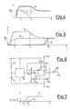
- Figs. 3-5 show curves representing voltage and current variation in time in the control circuit of Figs. 1 and 2;
- Fig. 6 shows a variant of the control circuit according to the invention, planned for use with an audio amplifier with double power supply;
- Fig. 7 shows a graph representing the variations in time of voltages and currents in the control circuit of Fig. 6.
- With reference to Fig. 1, A indicates an audio amplifier equipped with a positive input E, a negative input F and an output L for control of a loudspeaker AP. A feedback circuit between output L and input F includes a resistance R₅. A capacitor C₄ is inserted between the output L and the loudspeaker AP.
- The positive input E is connected by a resistance R₆ to a circuital node N connected to the main power supply Vcc and to earth by a resistance R₃ having a capacitor C₂ in parallel.
- The input E is also connected by a capacitor C₅ to an audio signal input lN, to which arrives the audio signal processed by the upstream circuits, generally represented and indicated by GS.
- The negative input F is in turn connected to the power supply Vcc through a current generator G₁ which generates a current I₁, and an earth through the series of a resistance R₄ and a capacitor C₃.
- Switching on of the amplifier A is provided for by a current generator G₂, which generates a switch-on current I₂.
- Current generators G₁ and G₂ are controlled by a circuital block B, which in turn is controlled by the voltage in a circuital node D connected to the power supply Vcc through a resistance R₁ and an earth through a capacitor C₁. In parallel with the latter is indicated a stand-by switch IS.
- A more detailed illustration of the circuital block B, as well as the generators G₁ and G₂ controlled by it, is given in Fig. 2, in which it is seen that circuital node D is connected to the base, connected to earth by a zener diode Z₁, of an n-p-n transistor T₁ the emitter of which is connected to earth through the series of a resistance R₇ and a diode D₁ and the collector connected to the positive power supply Vcc through a diode D₂.
- The collector of transistor T₁ is also connected to the base of a p-n-p transistor T₂, the emitter of which is connected to the power supply Vcc and the collector connected to the base of an n-p-n transistor T₈, the collector of which is connected to the power supply Vcc, the base connected to earth through a zener diode Z₂ and the emitter connected to earth through the series of two resistances R₈ and R₉ and a diode D₆.
- The base of transistor T₁ and a circuital node M intermediate between the two resistances R₈ and R₉ are connected, the first through a diode D₃ and the second directly, to the bases of their respective n-p-n transistors T₃ and T₇, which together form an oscillating circuit CB shiftable from one to the other of two operating states under the control of the voltages in nodes D and M.
- More precisely, the two transistors T₃ and T₇ have their respective emitters connected through equal resistances R₁₀ and R₁₁ to the collector of an n-p-n transistor T₆, the emitter of which is connected to earth and the base of which is connected to earth and of which the base is connected to a node intermediate between resistances R₉ and diode D₆. The collectors of transistors T₃ and T₇ are also connected to the positive power supply Vcc through their respective diodes D₄ and D₅.
- To the collectors of transistors T₃ and T₇ are also connected the bases of their respective p-n-p transistors T₄ and T₅, the emitters of which are connected to the power supply Vcc and perform the functions of the current generators G₂ and G₁ of Fig. 1, emitting the respective collector currents I₂ and I₁.
- The manner of operation of the control circuit of Figs. 1 and 2 can be understood with the help of the illustrative charts shown in Figs. 3-5. As shown in Fig. 3, from the moment of switching on of the equipment (t = 0) the positive power supply Vcc causes through resistance R₁ the gradual charging of capacitor C₁ and the consequent increase in the charging voltage VD (voltage in circuital node D) in accordance with the exponential curve shape shown in said figure. As long as VD remains below an intervention threshold represented by a value V₁ equal to the sum of the voltages VBE (base-emitter voltage) of the transistor T₁ and the diode D₁ the control circuit remains cut off and with it the audio amplifier A.
- At the moment when VD = V₁ occurs (instant T₀ in Fig. 3), T₁ is placed in conduction and through the mirror D₂ , T₂ causes switching on of the zener Z₂ and the consequent conduction of transistor T₈. In node M is therefore established a steady voltage VM, which puts the oscillating circuit CB in a first operating state in which transistor T₃ is cut off and transistor T₇ conducts, causing through D₅, T₅ the generation of a substantially constant current I₁. The current I₂ is substantially nil, transistor T₄ being of course cut off.
- As capacitor C₁ continues to be charged, when the charging voltage VD (instant T₁ in Fig. 3) reaches a value V₂ equal to VM less the voltage VBE of transistor T₇ and the voltage drop on R₁₁, plus the voltages VBE of transistor T₃ and diode D₃, transistor T₃ goes gradually into conduction, subtracting current from transistor T₇ and also causing through D₄, T₄ the generation of a current I₂, which increases in the same way that I₁ decreases, keeping the relation I₁ + I₂ = constant. The two currents, whose curve shape is shown in graphs I₁ and I₂ of Fig. 3, will be equal when VD reaches a value V₃ equal to VM plus the VBE of diode D₃ (instant T₂ in Fig. 3).
- As VD continues to increase, transistor T₇ goes gradually into cutoff, while T₃ reaches maximum conduction, and the oscillating circuit CB is consequently shifted into a second operating state in which I₁ is nil and I₂ has reached the maximum value shown in Fig. 3 (instant T₃).
- The described variation of currents I₁ and I₂ under the control of tie circuital block B causes the following behaviour of the audio amplifier A in response to the switching on of the equipment.
- The current generator G₁ is connected to the inverting input F of the amplifier A and starting from instant To charges with current I₁ gain capacitor C₃ up to a maximum value which remains substantially constant until the moment (instant T₃) when current I₁ is cancelled and capacitor C₃ consequently discharges progressively on resistance R₅, tending toward the value Vcc/2. The voltage curve (VF) to the above inverting input is shown in Fig. 4.
- The current generator G₂, which is assigned to switching on of the amplifier A, remains in turn cut off until instant T₁, consequently keeping the audio amplifier cut off. From instant T₁ it begins to deliver a progressively increasing current I₂, which gradually causes switching on of the amplifier, completing it at instant T₃.
- In the meantime however, as shown in Fig. 5, the inverting input F of the amplifier A was held at a voltage VF higher than that (VE) created by the noninverting input E from the polarization group R₂, R₃, RC (appropriately selected). Even with the amplifier switched on, the output voltage VL of the audio amplifier therefore remains nil and there is no signal at the loudspeaker AP.
- As shown in Fig. 5, voltage VL rises to a higher level only when voltage VF at the inverting input F falls to the level of voltage VE at the noninverting input E, that is at instant T₄. From that moment onward the audio amplifier begins to deliver current to the load, that is to the loudspeaker AP.
- The audio amplifier then becomes dynamic with a time delay T₄ after the instant the equipment is switched on. For all of this time the loudspeaker does not receive signals and hence does not produce sound. The upstream circuits, which generate the audio signal for the input lN, thus have time to settle.
- As already mentioned, the control circuit of Figs. 1 and 2 also provides for the possibility of placing the audio amplifier A, and the control circuit itself, in stand-by condition, that is in minimum current absorption condition. To achieve this it is sufficient to close the switch IS of Fig. 1, so as to bring about the discharge to earth of capacitor C₁. As can be, understood by observing Fig. 2, this causes the immediate cut-off of transistor T₁, and hence of transistor T₈, with the consequent return of the oscillating circuit CB to neutral position with both transistors T₃ and T₇ cut off and currents I₁ and I₂ of zero value. The audio amplifier A is thus cut off, as is the control circuit associated with it.
- Upon reopening of the switch 15, that is upon switching on again after stand-by, capacitor C₁ begins to recharge and the cycle described for delayed switching on again of the audio amplifier is repeated. Even in case of switching on again after stand-by, the transfer of the audio signals to the loudspeaker AP through the audio amplifier A is then delayed for the time necessary for the resettling of the audio signal generator circuits.
- The control circuit shown in Figs. 1 and 2 is suitable for the case of an audio amplifier with individual power supply.
- With two power supplies (+ Vcc; - Vcc) the control circuit may become simpler, and in particular generator G₁ and current I₁ can be eliminated. The control circuit can become as shown in Fig. 6 and the circuital block B can be simplified by directly connecting the collector of transistor T₇ to the power supply Vcc and eliminating D₅ and T₅.
- As shown in Fig. 6 the inverting input F of the audio amplifier is connected to earth through a resistance R₁₂ and the noninverting input of the amplifier is connected directly to the input IN and to earth through a resistance R₁₃.
- The operational result is shown in Fig. 7, which shows how current I₂ begins to increase at instant T₁ and then reaches operating value at instant T₂. At this point the amplifier A switches on, applying to the loudspeaker AP an ouput voltage VL corresponding to the audio signal at the input IN.
Claims (5)
- Audio amplifier switch-on control circuit in an audio signal generating apparatus, including a capacitor (C₁) progressively chargeable in response to the switching on of the apparatus, an oscillating circuit (CB) with intervention threshold, which responds to the increase in load voltage of said capacitor (C₁) beyond a preset value so as to shift progressively from a first to a second operating state for the generation of a switch-on current for the audio amplifier (A), and two commutating devices (T₁, T₈) associated with said oscillating circuit (CB), the first of which is controlled by the load voltage of said capacitor (C₁) and the second of which is controlled by the state of said first commutating device (T₁), said second commutating device (T₈) acting on said oscillating circuit (CB) so as to place it in said first operating state after said load voltage reaches said preset value, characterized in that said commutating devices (T₁, T₈) consist of transistors with intervention threshold and said oscillating circuit (CB) includes two opposed transistors (T₃, T₇), the first of which is controlled by said second commutating device (T₈) for placing said oscillating circuit (CB) in said operating state and the second of which is controlled by said first commutating device (T₁) for the progressive shifting of the oscillating circuit (CB) from said first to said second operating state.
- Control circuit according to claim 1, characterized in that said second transistor (T₇) controls a first current generator (G₂) for generation of the audio amplifier switch-on current.
- Control circuit according to claim 2, characterized in that said first transistor (T₇) controls a second current generator (G₁) for the generation of a charging current for a control capacitor (C₃) controlling the inverting input of the audio amplifier (A).
- Control circuit according to claim 3, characterized in that said control capacitor (C₃) is selected so as to achieve a load voltage which prevails over the polarization voltage of the non-inverting input of the audio amplifier (A) for a time longer than the switch-on time of the audio amplifier (A).
- Control circuit according to claim 1, characterized in that it includes a stand-by switch (IS) placed in parallel with said capacitor (C₁).
Applications Claiming Priority (2)
| Application Number | Priority Date | Filing Date | Title |
|---|---|---|---|
| IT2064584 | 1984-04-20 | ||
| IT8420645A IT1213158B (en) | 1984-04-20 | 1984-04-20 | IGNITION CONTROL CIRCUIT FOR AUDIO AMPLIFIER. |
Publications (3)
| Publication Number | Publication Date |
|---|---|
| EP0159079A2 EP0159079A2 (en) | 1985-10-23 |
| EP0159079A3 EP0159079A3 (en) | 1987-12-09 |
| EP0159079B1 true EP0159079B1 (en) | 1991-12-27 |
Family
ID=11169987
Family Applications (1)
| Application Number | Title | Priority Date | Filing Date |
|---|---|---|---|
| EP85200487A Expired EP0159079B1 (en) | 1984-04-20 | 1985-03-30 | Audio amplifier switch-on control circuit |
Country Status (4)
| Country | Link |
|---|---|
| US (1) | US4638507A (en) |
| EP (1) | EP0159079B1 (en) |
| DE (1) | DE3584988D1 (en) |
| IT (1) | IT1213158B (en) |
Families Citing this family (19)
| Publication number | Priority date | Publication date | Assignee | Title |
|---|---|---|---|---|
| JPH0618294B2 (en) * | 1987-02-27 | 1994-03-09 | 株式会社東芝 | Audio output amplifier |
| JP2547781B2 (en) * | 1987-07-13 | 1996-10-23 | 株式会社東芝 | BTL power amplifier circuit |
| JPH0642637B2 (en) * | 1988-08-12 | 1994-06-01 | 三洋電機株式会社 | Power save circuit for low frequency power amplification |
| IT1229860B (en) * | 1988-11-09 | 1991-09-13 | Sgs Thomson Microelectronics | INTEGRATED AUDIO AMPLIFIER WITH UNIFIED REGULATION OF "MUTE" AND "STAND BY" FUNCTIONS AND SWITCHING TRANSITORS. |
| US5029005A (en) * | 1990-04-25 | 1991-07-02 | Rca Licensing Corporation | Apparatus for the muting of an audio power amplifier in a standby mode |
| DE69231613T2 (en) * | 1992-05-22 | 2001-05-31 | Stmicroelectronics S.R.L., Agrate Brianza | Control circuit for switching an audio amplifier on and off |
| DE69209058T2 (en) * | 1992-05-29 | 1996-10-24 | Sgs Thomson Microelectronics | Switch-on control for electrical devices |
| DE4329638C2 (en) * | 1993-09-02 | 1996-10-24 | Telefunken Microelectron | Loudspeaker |
| USD398007S (en) | 1993-11-15 | 1998-09-08 | Gladstone Wilson | Wide range speaker unit |
| DE69406108T2 (en) * | 1994-04-15 | 1998-02-12 | St Microelectronics Srl | Low frequency amplifier |
| US5642076A (en) * | 1995-01-31 | 1997-06-24 | National Semiconductor Corporation | No turn-on pop noise amplifier |
| GB2361809B (en) | 1999-02-26 | 2003-11-05 | Trikon Holdings Ltd | A method of processing a polymer layer |
| DE69920404T2 (en) | 1999-05-14 | 2005-10-06 | Stmicroelectronics S.R.L., Agrate Brianza | Telephone receiving circuit for suppressing the circuit interference |
| WO2002015388A2 (en) * | 2000-08-11 | 2002-02-21 | Maxim Integrated Products, Inc. | Amplifier circuits and methods to provide smooth transition of amplifier outputs during powering sequences |
| US20040002780A1 (en) * | 2002-06-28 | 2004-01-01 | Ting-Yu Chang | Computer system with a preamplifier circuit mounted on a motherboard |
| DE602005011605D1 (en) * | 2004-05-17 | 2009-01-22 | Nxp Bv | PLUG NOISE AVOIDANCE FOR AN AMPLIFIER |
| US20060023896A1 (en) * | 2004-07-28 | 2006-02-02 | Ginsberg Mark G | Apparatus and method for controlling output signals from an amplifier when changing state |
| US20100272294A1 (en) * | 2007-12-21 | 2010-10-28 | The Tc Group A/S | Two-channel amplifier with common signal |
| US8818005B2 (en) * | 2011-05-17 | 2014-08-26 | Fairchild Semiconductor Corporation | Capacitor controlled switch system |
Family Cites Families (9)
| Publication number | Priority date | Publication date | Assignee | Title |
|---|---|---|---|---|
| JPS5539929B2 (en) * | 1972-05-10 | 1980-10-15 | ||
| US3965295A (en) * | 1974-07-17 | 1976-06-22 | Mcintosh Laboratory, Inc. | Protective system for stereo loudspeakers |
| JPS5935207B2 (en) * | 1979-07-27 | 1984-08-27 | ヤマハ株式会社 | power amplifier |
| JPS5717204A (en) * | 1980-07-04 | 1982-01-28 | Fujitsu Ltd | Transient sound prevention type power amplifying circuit |
| US4472687A (en) * | 1980-12-24 | 1984-09-18 | Tokyo Shibaura Denki Kabushiki Kaisha | Audio power amplifier for supplying electric power to a load by switching of power supply voltage |
| DE3108407A1 (en) * | 1981-03-06 | 1982-09-16 | Robert Bosch Gmbh, 7000 Stuttgart | "SOUND AUDIO" |
| IT1168164B (en) * | 1981-08-26 | 1987-05-20 | Ates Componenti Elettron | BRIDGE FINAL STAGE FOR AN AUDIO RECEPTION APPLICATOR |
| US4441086A (en) * | 1982-05-13 | 1984-04-03 | General Motors Corporation | Audio system with orderly shutdown sequence |
| US4453264A (en) * | 1982-09-23 | 1984-06-05 | Hochstein Peter A | Amplifier power supply controlled by audio signal |
-
1984
- 1984-04-20 IT IT8420645A patent/IT1213158B/en active
-
1985
- 1985-03-30 DE DE8585200487T patent/DE3584988D1/en not_active Expired - Lifetime
- 1985-03-30 EP EP85200487A patent/EP0159079B1/en not_active Expired
- 1985-04-12 US US06/722,386 patent/US4638507A/en not_active Expired - Lifetime
Also Published As
| Publication number | Publication date |
|---|---|
| IT1213158B (en) | 1989-12-14 |
| IT8420645A0 (en) | 1984-04-20 |
| US4638507A (en) | 1987-01-20 |
| EP0159079A3 (en) | 1987-12-09 |
| EP0159079A2 (en) | 1985-10-23 |
| DE3584988D1 (en) | 1992-02-06 |
Similar Documents
| Publication | Publication Date | Title |
|---|---|---|
| US4638507A (en) | Audio amplifier switch-on control circuit | |
| EP0383382B1 (en) | Power supply circuit | |
| KR0163762B1 (en) | Switch mode power supply | |
| US4983927A (en) | Integrated audio amplifier with combined regulation of the "mute" and "standby" functions and the switching transients | |
| US5495164A (en) | Boost converter | |
| US4819122A (en) | Over-current timer modulator | |
| JPH02273072A (en) | Electric source circuit | |
| US5363062A (en) | Audio amplifier on-off control circuit | |
| US5654626A (en) | Boost-converter with low losses | |
| US5101334A (en) | High speed power supply circuit with circuit with positive feedback | |
| JPS62268359A (en) | Power supply for video display equipment | |
| US4447791A (en) | Power supply changeover type power amplifier | |
| JPS589630B2 (en) | Circuit arrangement with high voltage power transistors | |
| EP0413749A1 (en) | Dual mode flyback power supply. | |
| GB2070369A (en) | Amplifier protection | |
| CA1169484A (en) | Direct current to alternating current converter | |
| US3622900A (en) | Squelchable direct coupled transistor audio amplifier constructed in integrated circuit | |
| JPS6339162B2 (en) | ||
| JPH0620167B2 (en) | Spurious signal reduction circuit | |
| JPS5837135Y2 (en) | Muting signal generation circuit | |
| JPH0549247A (en) | Switching power supply unit | |
| JPH03295472A (en) | Peak holding circuit | |
| US5075637A (en) | Control circuit for amplified listening | |
| JP3148551B2 (en) | Audio amplifier circuit | |
| JPS604306Y2 (en) | Tape recorder muting circuit |
Legal Events
| Date | Code | Title | Description |
|---|---|---|---|
| PUAI | Public reference made under article 153(3) epc to a published international application that has entered the european phase |
Free format text: ORIGINAL CODE: 0009012 |
|
| AK | Designated contracting states |
Designated state(s): DE FR GB NL |
|
| RAP1 | Party data changed (applicant data changed or rights of an application transferred) |
Owner name: SGS MICROELETTRONICA S.P.A. |
|
| PUAL | Search report despatched |
Free format text: ORIGINAL CODE: 0009013 |
|
| AK | Designated contracting states |
Kind code of ref document: A3 Designated state(s): DE FR GB NL |
|
| RAP1 | Party data changed (applicant data changed or rights of an application transferred) |
Owner name: SGS-THOMSON MICROELECTRONICS S.P.A. |
|
| 17P | Request for examination filed |
Effective date: 19880511 |
|
| RAP1 | Party data changed (applicant data changed or rights of an application transferred) |
Owner name: SGS-THOMSON MICROELECTRONICS S.R.L. |
|
| 17Q | First examination report despatched |
Effective date: 19900807 |
|
| GRAA | (expected) grant |
Free format text: ORIGINAL CODE: 0009210 |
|
| AK | Designated contracting states |
Kind code of ref document: B1 Designated state(s): DE FR GB NL |
|
| REF | Corresponds to: |
Ref document number: 3584988 Country of ref document: DE Date of ref document: 19920206 |
|
| ET | Fr: translation filed | ||
| PLBE | No opposition filed within time limit |
Free format text: ORIGINAL CODE: 0009261 |
|
| STAA | Information on the status of an ep patent application or granted ep patent |
Free format text: STATUS: NO OPPOSITION FILED WITHIN TIME LIMIT |
|
| 26N | No opposition filed | ||
| REG | Reference to a national code |
Ref country code: FR Ref legal event code: D6 |
|
| PGFP | Annual fee paid to national office [announced via postgrant information from national office to epo] |
Ref country code: FR Payment date: 20010313 Year of fee payment: 17 |
|
| PGFP | Annual fee paid to national office [announced via postgrant information from national office to epo] |
Ref country code: DE Payment date: 20010326 Year of fee payment: 17 |
|
| PGFP | Annual fee paid to national office [announced via postgrant information from national office to epo] |
Ref country code: GB Payment date: 20010328 Year of fee payment: 17 |
|
| PGFP | Annual fee paid to national office [announced via postgrant information from national office to epo] |
Ref country code: NL Payment date: 20010330 Year of fee payment: 17 |
|
| REG | Reference to a national code |
Ref country code: GB Ref legal event code: IF02 |
|
| PG25 | Lapsed in a contracting state [announced via postgrant information from national office to epo] |
Ref country code: GB Free format text: LAPSE BECAUSE OF NON-PAYMENT OF DUE FEES Effective date: 20020330 |
|
| PG25 | Lapsed in a contracting state [announced via postgrant information from national office to epo] |
Ref country code: NL Free format text: LAPSE BECAUSE OF NON-PAYMENT OF DUE FEES Effective date: 20021001 Ref country code: DE Free format text: LAPSE BECAUSE OF NON-PAYMENT OF DUE FEES Effective date: 20021001 |
|
| GBPC | Gb: european patent ceased through non-payment of renewal fee |
Effective date: 20020330 |
|
| PG25 | Lapsed in a contracting state [announced via postgrant information from national office to epo] |
Ref country code: FR Free format text: LAPSE BECAUSE OF NON-PAYMENT OF DUE FEES Effective date: 20021129 |
|
| NLV4 | Nl: lapsed or anulled due to non-payment of the annual fee |
Effective date: 20021001 |
|
| REG | Reference to a national code |
Ref country code: FR Ref legal event code: ST |