EP0154774A2 - Data transmission with a bidirectionel data bus - Google Patents
Data transmission with a bidirectionel data bus Download PDFInfo
- Publication number
- EP0154774A2 EP0154774A2 EP85100534A EP85100534A EP0154774A2 EP 0154774 A2 EP0154774 A2 EP 0154774A2 EP 85100534 A EP85100534 A EP 85100534A EP 85100534 A EP85100534 A EP 85100534A EP 0154774 A2 EP0154774 A2 EP 0154774A2
- Authority
- EP
- European Patent Office
- Prior art keywords
- data
- control unit
- peripheral
- addressed
- data bus
- Prior art date
- Legal status (The legal status is an assumption and is not a legal conclusion. Google has not performed a legal analysis and makes no representation as to the accuracy of the status listed.)
- Granted
Links
Images

Classifications
-
- G—PHYSICS
- G06—COMPUTING; CALCULATING OR COUNTING
- G06F—ELECTRIC DIGITAL DATA PROCESSING
- G06F13/00—Interconnection of, or transfer of information or other signals between, memories, input/output devices or central processing units
- G06F13/38—Information transfer, e.g. on bus
- G06F13/42—Bus transfer protocol, e.g. handshake; Synchronisation
- G06F13/4204—Bus transfer protocol, e.g. handshake; Synchronisation on a parallel bus
- G06F13/4208—Bus transfer protocol, e.g. handshake; Synchronisation on a parallel bus being a system bus, e.g. VME bus, Futurebus, Multibus
- G06F13/4217—Bus transfer protocol, e.g. handshake; Synchronisation on a parallel bus being a system bus, e.g. VME bus, Futurebus, Multibus with synchronous protocol
-
- H—ELECTRICITY
- H04—ELECTRIC COMMUNICATION TECHNIQUE
- H04Q—SELECTING
- H04Q9/00—Arrangements in telecontrol or telemetry systems for selectively calling a substation from a main station, in which substation desired apparatus is selected for applying a control signal thereto or for obtaining measured values therefrom
- H04Q9/14—Calling by using pulses
- H04Q9/16—Calling by using pulses by predetermined number of pulses
Definitions
- the invention is based on a data transmission between a control unit and via a clock line, an enable line and a data line connected to these individually addressable peripheral components for executing the commands issued by the control unit and for reporting data back to the control unit via a bidirectional data bus, the The peripheral blocks are addressed using the different word lengths of the data.
- control unit e.g. a microprocessor
- peripheral components connected to them in the form of integrated circuits for executing the commands issued by the control unit
- the control unit often requests feedback from the circuits addressed by it, so that the data flow on the data line must be possible in both directions.
- An arrangement in which a plurality of integrated circuits which can be addressed by a microprocessor are supplied with data via a data line.
- This is a system with a constant word length for addressing, data transmission and for the command to report data in the opposite direction. Due to the constant word length e.g. 8 bits in an 8 bit system result in very long commands, which take a corresponding amount of time to transmit. So you need e.g. for addressing, for the data and for the command for feedback, 8 bits each. The unnecessarily large word length is particularly disadvantageous for the last-mentioned command, since 8 bits must be transmitted due to the system, although a single bit would suffice.
- a data transmission system is also known in which the word length is variable and the peripheral modules are addressed using the word length determined.
- no bidirectional data bus is provided in this data transmission system.
- the object of the invention is to enable bidirectional data transmission between a control unit and a plurality of peripheral components connected to it, without providing a special command for this on the data line.
- the invention has the advantage that the data transmission is particularly fast since the time for the transmission of a special command is saved because the command is derived from the control signals of the control unit.
- the object on which the invention is based is achieved by the invention disclosed in the patent claim. Further advantageous possibilities for applying the invention result from the subclaims.
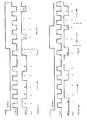
- the microprocessor 1 shows the control unit, for example a microprocessor, which corresponds to peripheral components 2, 3, 4 and 5.
- the microprocessor 1 has a connection labeled DATA, via which data can be sent to the peripheral components 2 to 5 and received by them via the bidirectional data line.
- the EN output activates the individual components 2 to 5 and synchronously with the clock signal CL the data is transferred.
- Each block 2 to 5 has a counter 8 or 9.
- the blocks are addressed in that a signal for accepting the data is sent via the EN input which is at H potential after the data has been input and which coincides with the counter output at H potential is derived in the corresponding module.
- the outputs Z1, Zn deliver signals after a different number of clock pulses CL. In this way, depending on the word length of the data, different modules can be addressed.
- the data stored in the catch register 6, 7 are at the inputs of the working memories 16 and 17 (latch) which, depending on the coincidence of the output signals of the counters 8 and 9, take over the data with the EN signal and put them at the outputs.
- the EN signal with L potential occurs, all counters are reset.
- a bistable flip-flop shown here as RS flip-flop 12 or 13 is set via the AND circuit 10 or 11, the output signals of which activate the response memory 14 or 15, which occurs when it arrives of clock pulses CL outputs the data to the control unit 1.
- the flip-flop 12 or 13 is reset again and the data flow from the response register 14 or 15 is prevented.
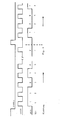
- FIG. 2 shows the case in which data from the control unit 1 are present at the data inputs of the peripheral modules 2 to 5. After the nth clock pulse there is an n-bit word in the catch registers of blocks 2 to 5. Block n, whose counter is set to the value n, takes the data into its working memory.
- the block to be addressed is determined using the positive edge of the EN signal. Immediately after this edge, the bits of the response to the data line 18 reach the control unit 1 in synchronism with the clock signal.
Abstract
Description
Die Erfindung geht aus von einer Datenübertragung zwischen einer Steuereinheit und über eine Clockleitung, eine Freigabeleitung und eine Datenleitung an diese angeschalteten einzeln adressierbaren Peripheriebausteinen zur Durchführung der von der Steuereinheit ausgegebenen Befehle und zur Rückmeldung von Daten an die Steuereinheit über einen bidirektional arbeitenden Datenbus, wobei die Adressierung der Peripheriebausteine über die unterschiedliche Wortlänge der Daten erfolgt.The invention is based on a data transmission between a control unit and via a clock line, an enable line and a data line connected to these individually addressable peripheral components for executing the commands issued by the control unit and for reporting data back to the control unit via a bidirectional data bus, the The peripheral blocks are addressed using the different word lengths of the data.
Bekanntlich findet zwischen einer Steuereinheit, wie z.B. einem Mikroprozessor, und den an diesen angeschalteten peripheren Bausteinen in Form von integrierten Schaltungen zur Ausführung der von der Steuereinheit abgegebenen Befehle ein ständiger Datenfluß statt. Die Steuereinheit verlangt dabei oftmals eine Rückmeldung von dem durch diese angesprochenen Schaltkreise, so daß der Datenfluß auf der Datenleitung in beiden Richtungen möglich sein muß.As is known, between a control unit, e.g. a microprocessor, and the peripheral components connected to them in the form of integrated circuits for executing the commands issued by the control unit, a constant data flow instead. The control unit often requests feedback from the circuits addressed by it, so that the data flow on the data line must be possible in both directions.
Es ist eine Anordnung bekannt, bei der mehrere von einem Mikroprozessor adressierbare integrierte Schaltungen mit Daten über eine Datenleitung beaufschlagt werden. Hierbei handelt es sich um ein System mit konstanter Wortlänge für die Adressierung, Datenübermittlung und für den Befehl zur Rückmeldung von Daten in umgekehrter Richtung. Durch die konstante Wortlänge z.B. 8 Bit bei einem 8-Bit-System ergeben sich sehr lange Befehle, für deren Übermittlung entsprechend viel Zeit beansprucht wird. So benötigt man z.B. für die Adressierung, für die Daten und für den Befehl zur Rückmeldung je 8 Bit. Insbesondere für den letztgenannten Befehl macht sich die unnötig große Wortlänge nachteilig bemerkbar, da systembedingt 8 Bit übertragen werden müssen, obwohl ein einziges Bit genügen würde.An arrangement is known in which a plurality of integrated circuits which can be addressed by a microprocessor are supplied with data via a data line. This is a system with a constant word length for addressing, data transmission and for the command to report data in the opposite direction. Due to the constant word length e.g. 8 bits in an 8 bit system result in very long commands, which take a corresponding amount of time to transmit. So you need e.g. for addressing, for the data and for the command for feedback, 8 bits each. The unnecessarily large word length is particularly disadvantageous for the last-mentioned command, since 8 bits must be transmitted due to the system, although a single bit would suffice.
Es ist außerdem ein Datenübertragungssystem bekannt, bei welchem mit variabler Wortlänge gearbeitet wird und die Adressierung der Peripheriebausteine über die ermittelte Wortlänge erfolgt. Jedoch ist bei diesem Datenübertragungssystem kein bidirektionaler Datenbus vorgesehen.A data transmission system is also known in which the word length is variable and the peripheral modules are addressed using the word length determined. However, no bidirectional data bus is provided in this data transmission system.
Der Erfindung liegt die Aufgabe zugrunde, eine bidirektionale Datenübertragung zwischen einer Steuereinheit und mehreren an diese angeschalteten Peripheribausteinen zu ermöglichen, ohne auf der Datenleitung einen besonderen Befehl dafür vorzusehen. Die Erfindung bringt den Vorteil, daß die Datenübertragung besonders schnell wird, da die Zeit zur Übermittlung eines besonderen Befehls eingespart wird, weil der Befehl aus den Steuersignalen der Steuereinheit abgeleitet wird. Die der Erfindung zugrunde liegende Aufgabe wird durch die im Patentanspruch offenbarte Erfindung gelöst. Weitere vorteilhafte Möglichkeiten zur Anwendung der Erfindung ergeben sich aus den Unteransprüchen.The object of the invention is to enable bidirectional data transmission between a control unit and a plurality of peripheral components connected to it, without providing a special command for this on the data line. The invention has the advantage that the data transmission is particularly fast since the time for the transmission of a special command is saved because the command is derived from the control signals of the control unit. The object on which the invention is based is achieved by the invention disclosed in the patent claim. Further advantageous possibilities for applying the invention result from the subclaims.
Nachstehend soll die Erfindung an einem Ausführungsbeispiel mit Hilfe der Zeichnung erläutert werden, wobei in
Figur 1 ein die Erfindung beschreibendes Blockschaltbild und dieFiguren 2 bis 4 Beispiele für die Datenübertragung zeigen.
- Figure 1 is a block diagram describing the invention and the
- Figures 2 to 4 show examples of data transmission.
Mit 1 ist die Steuereinheit, z.B. einMikroprozessor, gezeigt, der mit Peripheriebausteinen 2, 3, 4 und 5 korrespondiert. Der Mikroprozessor 1 besitzt einen mit DATA bezeichneten Anschluß, über welchen Daten an die Peripheriebausteine 2 bis 5 abgegeben und von diesen über die bidirektionale Datenleitung empfangen werden können.Der EN-Ausgang aktiviert die einzelnen Bauteine 2 bis 5 und synchron mit dem Clock-Signal CL werden die Daten transferiert. Jeder Baustein 2 bis 5 besitzt einen Zähler 8 bzw. 9. Die Adressierung der Bausteine erfolgt dadurch, daß über den nach der Dateneingabe auf H-Potential liegenden EN-Eingang in Koinzidenz mit dem auf H-Potential liegenden Zählerausgang ein Signal zur Übernahme der Daten in dem entsprechenden Baustein abgeleitet wird. Die AusgängeZ1, Zn liefern-Signale nach verschiedener Anzahl von Clock-Impulsen CL.Auf diese Weise sind je nach Wortlänge der Daten verschiedenen Bausteine adressierbar. Die im Auffangregister 6, 7 gespeicherten Daten liegen an den Eingängen von Arbeitsspeichern 16 und 17 (Latch) die je nach Koinzidenz der Ausgangssignale der Zähler 8 bzw. 9 mit dem EN-Signal die Daten übernehmen und an die Ausgänge legen. Mit Auftreten des EN-Signals mit L-Potential werden sämtliche Zähler zurückgesetzt. Unmittelbar nach der Datenausgabe von der Steuerschaltung 1 wird über die Und-Schaltung 10 bzw. 11 eine bistabile Kippstufe, hier als R-S-Flip -Flop 12 bzw. 13 dargestellt, gesetzt, deren Ausgangssignale den Antwortspeicher 14 bzw. 15 aktivieren, der bei Eintreffen von Clockimpulsen CL die Daten an die Steuereinheit 1 ausgibt. Sobald das EN-Signal bei Eintreffen von Daten aus der Steuereinheit 1 auf Null-Potential liegt, wird das Flip -Flop 12 bzw. 13 wieder zurückgesetzt und der Datenfluß aus dem Antwortregister 14 bzw. 15 unterbunden.1 shows the control unit, for example a microprocessor, which corresponds to
Mit Hilfe der nachfolgenden Figuren 2 bis 4 werden verschiedene Arten des Datenflußes beschrieben.Various types of data flow are described with the aid of the following FIGS. 2 to 4.
In Figur 2 ist der Fall gezeigt, daß Daten von der Steuereinheit 1 an den Dateneingängen der Peripheriebausteine 2 bis 5 anliegen. Nach dem n-ten Clockimpuls liegt ein n-Bit-Wort in den Auffangregistern der Bausteine 2 bis 5. Der Baustein n, dessen Zähler auf den Wert n eingestellt ist, übernimmt die Daten in seinen Arbeitsspeicher.FIG. 2 shows the case in which data from the
Der zu adressierende Baustein wird mit Hilfe der positiven Flanke des EN-Signals bestimmt. Unmittelbar nach dieser Flanke gelangen synchron zum Clocksignal die Bits der Antwort auf die Datenleitung 18 zur Steuerinheit 1.The block to be addressed is determined using the positive edge of the EN signal. Immediately after this edge, the bits of the response to the
Im Fall von Figur 3 sei für die Steuereinheit 1 nur der Wert des erten und zweiten Datenbits für die Rückmeldung wichtig. Durch das EN-Signal kann somit die Antwort sofort nach Eintreffen des zweiten Bits unterbunden werden. Dies hat den Vorteil, daß die Steuereinheit 1 sofort neue Daten senden kann, wodurch Zeit gespart wird.In the case of FIG. 3, only the value of the first and second data bits for the feedback is important for the
Nach Figur 4 ist keine Antwort erforderlich. Der Datenfluß in umgekehrter Richtung wird völlig unterdrückt, indem das EN-Signal nach Eintreffen und Verarbeiten des ersten Wortes sofort wieder auf niedriges Potential geht, so daß unmittelbar das nächstfolgende Wort von der Steuereinheit 1 auf die Datenleitung 18 gegeben wird. Dieses bringt den Vorteil, daß bei Befehlen, die keine Antwort für die Steuereinheit benötigen, keine zusätzliche Zeit verloren geht. Somit ist die Datenleitung sofort frei für die Übermittlung von Daten aus der Steuereinheit.According to FIG. 4, no answer is required. The data flow in the reverse direction is completely suppressed by the EN signal immediately returning to a low potential after the arrival and processing of the first word, so that the next word from
Claims (1)
Priority Applications (1)
| Application Number | Priority Date | Filing Date | Title |
|---|---|---|---|
| AT85100534T ATE77724T1 (en) | 1984-02-10 | 1985-01-19 | DATA TRANSMISSION WITH BIDIRECTIONAL DATA BUS. |
Applications Claiming Priority (2)
| Application Number | Priority Date | Filing Date | Title |
|---|---|---|---|
| DE3404721 | 1984-02-10 | ||
| DE3404721A DE3404721C2 (en) | 1984-02-10 | 1984-02-10 | Circuit arrangement for the transmission of data |
Publications (3)
| Publication Number | Publication Date |
|---|---|
| EP0154774A2 true EP0154774A2 (en) | 1985-09-18 |
| EP0154774A3 EP0154774A3 (en) | 1988-10-05 |
| EP0154774B1 EP0154774B1 (en) | 1992-06-24 |
Family
ID=6227325
Family Applications (1)
| Application Number | Title | Priority Date | Filing Date |
|---|---|---|---|
| EP85100534A Expired - Lifetime EP0154774B1 (en) | 1984-02-10 | 1985-01-19 | Data transmission with a bidirectionel data bus |
Country Status (5)
| Country | Link |
|---|---|
| EP (1) | EP0154774B1 (en) |
| JP (1) | JPH06100997B2 (en) |
| AT (1) | ATE77724T1 (en) |
| DE (2) | DE3404721C2 (en) |
| HK (1) | HK15396A (en) |
Cited By (1)
| Publication number | Priority date | Publication date | Assignee | Title |
|---|---|---|---|---|
| EP0434083A2 (en) * | 1989-12-21 | 1991-06-26 | Kabushiki Kaisha Toshiba | Data transfer system and method of transferring data |
Families Citing this family (1)
| Publication number | Priority date | Publication date | Assignee | Title |
|---|---|---|---|---|
| DE3829454A1 (en) * | 1988-08-31 | 1990-03-01 | Thomson Brandt Gmbh | SERIAL DATA INTERFACE |
Citations (3)
| Publication number | Priority date | Publication date | Assignee | Title |
|---|---|---|---|---|
| GB1221964A (en) * | 1967-04-18 | 1971-02-10 | Ibm | Data transmission system |
| JPS5735446A (en) * | 1980-08-11 | 1982-02-26 | Omron Tateisi Electronics Co | Data transmission system |
| JPS5761362A (en) * | 1980-09-30 | 1982-04-13 | Nissan Motor Co Ltd | Transmitter/receiver unit |
-
1984
- 1984-02-10 DE DE3404721A patent/DE3404721C2/en not_active Expired - Lifetime
-
1985
- 1985-01-19 AT AT85100534T patent/ATE77724T1/en not_active IP Right Cessation
- 1985-01-19 DE DE8585100534T patent/DE3586252D1/en not_active Expired - Fee Related
- 1985-01-19 EP EP85100534A patent/EP0154774B1/en not_active Expired - Lifetime
- 1985-02-08 JP JP60022071A patent/JPH06100997B2/en not_active Expired - Lifetime
-
1996
- 1996-01-25 HK HK15396A patent/HK15396A/en not_active IP Right Cessation
Patent Citations (3)
| Publication number | Priority date | Publication date | Assignee | Title |
|---|---|---|---|---|
| GB1221964A (en) * | 1967-04-18 | 1971-02-10 | Ibm | Data transmission system |
| JPS5735446A (en) * | 1980-08-11 | 1982-02-26 | Omron Tateisi Electronics Co | Data transmission system |
| JPS5761362A (en) * | 1980-09-30 | 1982-04-13 | Nissan Motor Co Ltd | Transmitter/receiver unit |
Non-Patent Citations (2)
| Title |
|---|
| PATENT ABSTRACTS OF JAPAN, Band 6, Nr. 103 (E-112)[981], 12. Juni 1982; & JP-A-57 35 446 (TATEISHI DENKI K.K.) 26-02-1982 * |
| PATENT ABSTRACTS OF JAPAN, Band 6, Nr. 136 (E-120)[1014], 23. Juli 1982; & JP-A-57 61 362 (NISSAN JIDOSHA K.K.) 13-04-1982 * |
Cited By (2)
| Publication number | Priority date | Publication date | Assignee | Title |
|---|---|---|---|---|
| EP0434083A2 (en) * | 1989-12-21 | 1991-06-26 | Kabushiki Kaisha Toshiba | Data transfer system and method of transferring data |
| EP0434083A3 (en) * | 1989-12-21 | 1992-03-04 | Kabushiki Kaisha Toshiba | Data transfer system and method of transferring data |
Also Published As
| Publication number | Publication date |
|---|---|
| EP0154774B1 (en) | 1992-06-24 |
| ATE77724T1 (en) | 1992-07-15 |
| DE3404721C2 (en) | 1991-07-25 |
| EP0154774A3 (en) | 1988-10-05 |
| DE3586252D1 (en) | 1992-07-30 |
| HK15396A (en) | 1996-02-02 |
| DE3404721A1 (en) | 1985-08-14 |
| JPH06100997B2 (en) | 1994-12-12 |
| JPS60209864A (en) | 1985-10-22 |
Similar Documents
| Publication | Publication Date | Title |
|---|---|---|
| DE2457553C2 (en) | Asynchronous clock device | |
| DE3300260C2 (en) | ||
| DE3300261C2 (en) | ||
| DE2157982A1 (en) | Digital multiprocessor data processing system | |
| DE3418248A1 (en) | DATA PROCESSING SYSTEM WITH AN ARRANGEMENT FOR DATA TRANSFER BETWEEN A STORAGE AND A CENTRAL PROCESSOR | |
| DE2406740A1 (en) | PROCESS EQUIPMENT REGULATION SYSTEM | |
| EP0006164A1 (en) | Multiprocessor system with jointly usable storages | |
| DE3508321A1 (en) | PROGRAMMABLE CIRCUIT FOR CONTROLLING A LIQUID CRYSTAL DISPLAY | |
| DE3501194C2 (en) | Method and device for data exchange between microprocessors | |
| DE4005042A1 (en) | ARCHITECTURE OF A HIGH-SPEED DIGITAL MOTION CONTROL | |
| DE3042105C2 (en) | ||
| DE2154488A1 (en) | Data transmission sub-channel of a data processing system | |
| EP0154774B1 (en) | Data transmission with a bidirectionel data bus | |
| DE2442673C2 (en) | Device for inserting control data into the voice memory of a time division switch | |
| EP0037074B1 (en) | Method and circuit for the reception and transmission of information and signalling data in a programme-controlled data switching exchange | |
| DE3139421A1 (en) | Serial output circuit | |
| DE19948598B4 (en) | Microcomputer with sampling function of a repeat request signal in synchronization with a sampling signal | |
| DE3248276C2 (en) | ||
| DE3826266C2 (en) | ||
| EP0356873B1 (en) | Serial data interface | |
| DE3104928C2 (en) | Multi-microcomputer system with direct memory access | |
| EP0301160A2 (en) | System with two microprocessors and shared write/read memory | |
| DE3214576C2 (en) | Circuit arrangement for determining permanent position signals on connecting lines of a switching system | |
| DE2756764C3 (en) | Device for the synchronization of processor and memory in an electronic data processing system | |
| DE1800139C3 (en) | Input / output control unit for an electronic computer |
Legal Events
| Date | Code | Title | Description |
|---|---|---|---|
| PUAI | Public reference made under article 153(3) epc to a published international application that has entered the european phase |
Free format text: ORIGINAL CODE: 0009012 |
|
| AK | Designated contracting states |
Designated state(s): AT CH DE FR GB IT LI NL SE |
|
| PUAL | Search report despatched |
Free format text: ORIGINAL CODE: 0009013 |
|
| AK | Designated contracting states |
Kind code of ref document: A3 Designated state(s): AT CH DE FR GB IT LI NL SE |
|
| 17P | Request for examination filed |
Effective date: 19890313 |
|
| 17Q | First examination report despatched |
Effective date: 19910219 |
|
| GRAA | (expected) grant |
Free format text: ORIGINAL CODE: 0009210 |
|
| AK | Designated contracting states |
Kind code of ref document: B1 Designated state(s): AT CH DE FR GB IT LI NL SE |
|
| REF | Corresponds to: |
Ref document number: 77724 Country of ref document: AT Date of ref document: 19920715 Kind code of ref document: T |
|
| ITF | It: translation for a ep patent filed |
Owner name: BARZANO' E ZANARDO MILANO S.P.A. |
|
| GBT | Gb: translation of ep patent filed (gb section 77(6)(a)/1977) | ||
| REF | Corresponds to: |
Ref document number: 3586252 Country of ref document: DE Date of ref document: 19920730 |
|
| ET | Fr: translation filed | ||
| ET1 | Fr: translation filed ** revision of the translation of the patent or the claims | ||
| PLBE | No opposition filed within time limit |
Free format text: ORIGINAL CODE: 0009261 |
|
| STAA | Information on the status of an ep patent application or granted ep patent |
Free format text: STATUS: NO OPPOSITION FILED WITHIN TIME LIMIT |
|
| 26N | No opposition filed | ||
| EAL | Se: european patent in force in sweden |
Ref document number: 85100534.8 |
|
| PGFP | Annual fee paid to national office [announced via postgrant information from national office to epo] |
Ref country code: GB Payment date: 19960105 Year of fee payment: 12 |
|
| PGFP | Annual fee paid to national office [announced via postgrant information from national office to epo] |
Ref country code: FR Payment date: 19960115 Year of fee payment: 12 |
|
| PGFP | Annual fee paid to national office [announced via postgrant information from national office to epo] |
Ref country code: SE Payment date: 19960126 Year of fee payment: 12 Ref country code: AT Payment date: 19960126 Year of fee payment: 12 |
|
| PGFP | Annual fee paid to national office [announced via postgrant information from national office to epo] |
Ref country code: NL Payment date: 19960129 Year of fee payment: 12 |
|
| PGFP | Annual fee paid to national office [announced via postgrant information from national office to epo] |
Ref country code: CH Payment date: 19960206 Year of fee payment: 12 |
|
| PGFP | Annual fee paid to national office [announced via postgrant information from national office to epo] |
Ref country code: DE Payment date: 19960316 Year of fee payment: 12 |
|
| PG25 | Lapsed in a contracting state [announced via postgrant information from national office to epo] |
Ref country code: GB Effective date: 19970119 Ref country code: AT Effective date: 19970119 |
|
| PG25 | Lapsed in a contracting state [announced via postgrant information from national office to epo] |
Ref country code: SE Effective date: 19970120 |
|
| PG25 | Lapsed in a contracting state [announced via postgrant information from national office to epo] |
Ref country code: LI Effective date: 19970131 Ref country code: CH Effective date: 19970131 |
|
| PG25 | Lapsed in a contracting state [announced via postgrant information from national office to epo] |
Ref country code: NL Effective date: 19970801 |
|
| GBPC | Gb: european patent ceased through non-payment of renewal fee |
Effective date: 19970119 |
|
| REG | Reference to a national code |
Ref country code: CH Ref legal event code: PL |
|
| PG25 | Lapsed in a contracting state [announced via postgrant information from national office to epo] |
Ref country code: FR Effective date: 19970930 |
|
| NLV4 | Nl: lapsed or anulled due to non-payment of the annual fee |
Effective date: 19970801 |
|
| PG25 | Lapsed in a contracting state [announced via postgrant information from national office to epo] |
Ref country code: DE Effective date: 19971001 |
|
| EUG | Se: european patent has lapsed |
Ref document number: 85100534.8 |
|
| REG | Reference to a national code |
Ref country code: FR Ref legal event code: ST |