EP0151248A2 - High voltage circuit - Google Patents
High voltage circuit Download PDFInfo
- Publication number
- EP0151248A2 EP0151248A2 EP84114211A EP84114211A EP0151248A2 EP 0151248 A2 EP0151248 A2 EP 0151248A2 EP 84114211 A EP84114211 A EP 84114211A EP 84114211 A EP84114211 A EP 84114211A EP 0151248 A2 EP0151248 A2 EP 0151248A2
- Authority
- EP
- European Patent Office
- Prior art keywords
- transistor
- high voltage
- current electrode
- signal
- coupled
- Prior art date
- Legal status (The legal status is an assumption and is not a legal conclusion. Google has not performed a legal analysis and makes no representation as to the accuracy of the status listed.)
- Withdrawn
Links
Images
Classifications
-
- H—ELECTRICITY
- H03—ELECTRONIC CIRCUITRY
- H03K—PULSE TECHNIQUE
- H03K19/00—Logic circuits, i.e. having at least two inputs acting on one output; Inverting circuits
- H03K19/01—Modifications for accelerating switching
- H03K19/017—Modifications for accelerating switching in field-effect transistor circuits
- H03K19/01707—Modifications for accelerating switching in field-effect transistor circuits in asynchronous circuits
- H03K19/01721—Modifications for accelerating switching in field-effect transistor circuits in asynchronous circuits by means of a pull-up or down element
-
- H—ELECTRICITY
- H02—GENERATION; CONVERSION OR DISTRIBUTION OF ELECTRIC POWER
- H02M—APPARATUS FOR CONVERSION BETWEEN AC AND AC, BETWEEN AC AND DC, OR BETWEEN DC AND DC, AND FOR USE WITH MAINS OR SIMILAR POWER SUPPLY SYSTEMS; CONVERSION OF DC OR AC INPUT POWER INTO SURGE OUTPUT POWER; CONTROL OR REGULATION THEREOF
- H02M3/00—Conversion of dc power input into dc power output
- H02M3/02—Conversion of dc power input into dc power output without intermediate conversion into ac
- H02M3/04—Conversion of dc power input into dc power output without intermediate conversion into ac by static converters
- H02M3/10—Conversion of dc power input into dc power output without intermediate conversion into ac by static converters using discharge tubes with control electrode or semiconductor devices with control electrode
- H02M3/145—Conversion of dc power input into dc power output without intermediate conversion into ac by static converters using discharge tubes with control electrode or semiconductor devices with control electrode using devices of a triode or transistor type requiring continuous application of a control signal
- H02M3/155—Conversion of dc power input into dc power output without intermediate conversion into ac by static converters using discharge tubes with control electrode or semiconductor devices with control electrode using devices of a triode or transistor type requiring continuous application of a control signal using semiconductor devices only
-
- H—ELECTRICITY
- H03—ELECTRONIC CIRCUITRY
- H03F—AMPLIFIERS
- H03F3/00—Amplifiers with only discharge tubes or only semiconductor devices as amplifying elements
- H03F3/34—Dc amplifiers in which all stages are dc-coupled
- H03F3/343—Dc amplifiers in which all stages are dc-coupled with semiconductor devices only
- H03F3/345—Dc amplifiers in which all stages are dc-coupled with semiconductor devices only with field-effect devices
-
- H—ELECTRICITY
- H03—ELECTRONIC CIRCUITRY
- H03K—PULSE TECHNIQUE
- H03K19/00—Logic circuits, i.e. having at least two inputs acting on one output; Inverting circuits
- H03K19/0175—Coupling arrangements; Interface arrangements
- H03K19/0185—Coupling arrangements; Interface arrangements using field effect transistors only
Definitions
- This invention relates to high voltage circuits, and more particularly, to high voltage circuits controlled by a logic signal.
- EEPROMs electrically erasable programmable read only memories
- the high voltage can be either externally applied or internally generated.
- An internally generated high voltage although requiring more circuitry, is much more convenient for the end user.
- the current capability is limited.
- the EEPROM cells do require some current, however, for programming. Consequently, efficient use of the high voltage power supply current under the control of a logic signal is required.
- each pump circuit requires a clock signal in addition to the control logic signal. Also, each pump circuit requires substantial chip area in order to obtain sufficient current.
- An object of the present invention is to provide an improved high voltage circuit.
- Another object of the invention is to provide a high voltage circuit with increased current capability.
- Yet another object of the invention is to provide a high voltage circuit requiring less chip area.
- a high voltage circuit which has first transistor and second transistors, and a load.
- the first transistor has a first current electrode coupled to a first power supply terminal, a control electrode for receiving an input signal, and a second current electrode.
- the load is coupled between an output node and the second current electrode of the first transistor.
- the second transistor has a first current electrode coupled to a high voltage power supply terminal, a second current electrode coupled to the second current electrode of the first power supply terminal, and a control electrode coupled to the output Inode.
- Transistor 11-15 are N channel insulated gate field effect transistors.
- Transistor 11 is preferably enhancement mode with a threshold voltage of 0.6 to 0.9 volt.
- Transistors 12 and 13 are preferrably natural, also called zero threshold devices, with a threshold voltage of 0 to 0.4 volt.
- Transistor 14 is preferably heavy depletion with a threshold voltage of 3.2 to -3.6 volts.
- Transistor 15 is preferably light depletion with a threshold voltage of -2.2 to -2.6 volts.
- Transistor 11 has a gate for receiving a signal VI, a source connected to ground, and a drain for providing signal VO.
- Transistor 12 has a drain connected to a positive power supply terminal Vcc for receiving, for example, 5 volts, a source connected to the drain of transistor 11, and a gate.
- Inverter 16 has an input for receiving signal VI, and an output connected to the gate of transistor 12.
- Transistors 11 and 12 and inverter 16 together form an inverting push-pull buffer.
- Transistor 13 has a gate for receiving signal VI, a drain connected to Vcc, and a source.
- Transistor 14 has a drain connected to the source of transistor 13, and a gate and a source connected to the drain of transistor 11.
- Transistor 15 has a gate connected to the source and gate of transistor 14, a source connected to the drain of transistor 14, and a drain connected to a . high voltage power supply terminal for receiving, for example, 18 volts.
- transistor 11 When signal VI is a logic high, transistor 11 is conducting, causing signal VO to be a logic low at essentially ground potential. With signal VI at a logic high, transistor 13 is conducting so a positive voltage is generated on the source of transistor 13 and the drain of transistor 14 of sufficient magnitude to ensure that transistor 15 is not conducting. In view of transistor 15 being light depletion the lowest threshold voltage, highest in magnitude, it can have is -2.6 volts. Consequently transistor 15 will not be conducting so long as the voltage on its source exceeds the voltage on its gate by 2.6 volts. With transistor 14 having its gate and source connected together it acts as a load device so that with transistors 11 and 13 conducting there is a current path through transistors 13, 14 and 11.
- Transistor 11 is made of sufficiently high gain that signal VO will not exceed several tenths of a volt, for example 0.3 volt. With the gate of transistor 15 ensured of being at no more than 0.3 volt, transistor 15 is ensured of not conducting so long as its source exceeds 2.9 volts.
- Signal VI will typically be a buffered signal so that its voltage at a logic high will be known and is preferably very near the voltage at Vcc. When signal VI is at a logic high, transistor 15 is not conducting so that there is then no current drain on the high voltage power supply at Vpp. The only current drain is from Vcc which receives voltage from an external power supply. The current drain for such an external power supply is quite small.
- Inverter 16 supplies a logic high to the gate of transistor 12 causing it to become conducting and cause signal VO to increase in voltage sufficiently to cause transistor 15 to become conducting. A regenerative process is thereby started. With transistor 15 conducting, the source of transistor 15 will increase to a voltage above that at its gate, which is then coupled back to the gate of transistor 15 via transistor 14 so that further voltage increases on the source of transistor 15 can occur with all such increases coupled back to the gate of transistor 15 via transistor 14. Such regenerative action continues until signal VO reaches the voltage at Vpp less the voltage drop through transistors 14 and 15 due to current flow therethrough.
- the gains of transistors 14 and 15 are chosen so that there is very little voltage drop due to the current flow.
- the output impedance of the high voltage power supply which supplies the voltage to Vpp is typically relatively large so that voltage reduction of signal VO due to current flow is caused mostly by the high output impedance of the power supply rather than the loading effect of transistors 14 and 15.
- the high voltage supply is assumed to be an internal supply which uses switching techniques to obtain a high voltage from 5 volts and as such has a limited current supplying capability.
- the gain of transistor 14 must be sufficiently large to prevent loading the power supply, the chip area required for high voltage circuit 10 is less than that required for a pump type circuit of comparable current carrying capability.
- FIG. 2 Shown in Figure 2 is a high voltage circuit 10' which is the same as high voltage circuit 10 of Figure 1, except that a transistor 17 is interposed between the drain of transistor 11 and the source and gate of transistor 14 and the gate of transistor 15, and a transistor 18 is interposed between the source of transistor 11 and ground.
- Transistor 17 has a gate connected to Vpp, a drain connected to the source and gate of transistor 14 and the gate of transistor 15, and a source connected to the drain of transistor 11.
- Transistor 18 has a drain connected to the source of transistor 11, a source connected to ground, and a gate for receiving a write signal W.
- Transistor 17, as is transistor 13, is a natural.
- Transistor 18, as is transistor 11, is an enhancement.
- Transistor 17 is added to block current flow when the high voltage at Vpp is at ground potential. Because it is an internally generated voltage, it need not be generated at all times. There are times, such as a read mode of a memory, in which a high voltage is not required. During such a mode, power can be saved by not generating the high voltage. In such a read mode, Vpp at ground potential is used to advantage to make transistor 17 non-conducting. When signal VO is used for writing into an EEPROM cell, signal VO is coupled to the same line that is used for sensing data in the read mode. Consequently, in the read mode, it is necessary for circuit 10' to not interfere with the sensing of data. Transistor 17 effectively prevents transistors 13-15 from influencing such data sensing.
- Transistor 18 is conducting only when signal W is a logic high which is in the write mode. In the read mode signal W is a logic low so that transistor 18 is non-conducting. Transistor 18 thereby blocks a path to ground. Signal VI is ensured of being a logic high during the read mode. Consequently, inverter 16 provides a logic low to the gate of transistor 12, causing transistor 12 to be non-conducting. Consequently, circuit 10' does not influence the sensing of data during the read mode.
- Circuit 10 of Figure 1 provides a high voltage signal responsive to a 5 volt logic signal.
- Circuit 10' also provides a high voltage signal responsive to a 5 volt logic signal with the added feature of being useful for supplying the high voltage signal into an input/output node.
- Transistors 17 and 18 do not interfere with the normal operation of circuit 10'. When Vpp is at a high voltage, transistor 17 provides only negligible resistance between its source and drain so that the regenerative operation of transistors 14 and 15 results in the same voltage level for signal VO as that supplied by circuit 10 of Figure 1.
- transistor 18 receives a logic high on its gate causing it to be conductive. With transistor 18 conducting, transistor 11 responds in the same way as in circuit 10 of Figure 1.
Landscapes
- Engineering & Computer Science (AREA)
- Computer Hardware Design (AREA)
- Physics & Mathematics (AREA)
- Computing Systems (AREA)
- General Engineering & Computer Science (AREA)
- Mathematical Physics (AREA)
- Power Engineering (AREA)
- Logic Circuits (AREA)
- Transforming Light Signals Into Electric Signals (AREA)
- Amplifiers (AREA)
- Dc-Dc Converters (AREA)
- Read Only Memory (AREA)
Abstract
Description
- This invention relates to high voltage circuits, and more particularly, to high voltage circuits controlled by a logic signal.
- In electrically erasable programmable read only memories (EEPROMs) a high voltage is required to program and erase. The high voltage can be either externally applied or internally generated. An internally generated high voltage, although requiring more circuitry, is much more convenient for the end user. For such internally generated high voltage, the current capability is limited. The EEPROM cells do require some current, however, for programming. Consequently, efficient use of the high voltage power supply current under the control of a logic signal is required.
- This typically has been done by using another pump circuit for each high voltage signal to be generated in conjunction with the high voltage separately generated. This requires a clock signal in addition to the control logic signal. Also, each pump circuit requires substantial chip area in order to obtain sufficient current.
- An object of the present invention is to provide an improved high voltage circuit.
- Another object of the invention is to provide a high voltage circuit with increased current capability.
- Yet another object of the invention is to provide a high voltage circuit requiring less chip area.
- These and other objects are achieved in a high voltage circuit which has first transistor and second transistors, and a load. The first transistor has a first current electrode coupled to a first power supply terminal, a control electrode for receiving an input signal, and a second current electrode. The load is coupled between an output node and the second current electrode of the first transistor. The second transistor has a first current electrode coupled to a high voltage power supply terminal, a second current electrode coupled to the second current electrode of the first power supply terminal, and a control electrode coupled to the output Inode.
-
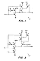
- Figure 1 is a circuit diagram of a high voltage circuit according to a preferred embodiment of the invention; and
- Figure 2 is a circuit diagram of a high voltage circuit which includes a modification of the high voltage circuit of Figure 1.
- Shown in Figure 1 is a
high voltage circuit 10 comprised of a transistor 11, atransistor 12, atransistor 13, atransistor 14, atransistor 15, and aninverter 16. Transistors 11-15 are N channel insulated gate field effect transistors. Transistor 11 is preferably enhancement mode with a threshold voltage of 0.6 to 0.9 volt.Transistors Transistor 14 is preferably heavy depletion with a threshold voltage of 3.2 to -3.6 volts.Transistor 15 is preferably light depletion with a threshold voltage of -2.2 to -2.6 volts. - Transistor 11 has a gate for receiving a signal VI, a source connected to ground, and a drain for providing signal VO.
Transistor 12 has a drain connected to a positive power supply terminal Vcc for receiving, for example, 5 volts, a source connected to the drain of transistor 11, and a gate.Inverter 16 has an input for receiving signal VI, and an output connected to the gate oftransistor 12.Transistors 11 and 12 and inverter 16 together form an inverting push-pull buffer.Transistor 13 has a gate for receiving signal VI, a drain connected to Vcc, and a source.Transistor 14 has a drain connected to the source oftransistor 13, and a gate and a source connected to the drain of transistor 11.Transistor 15 has a gate connected to the source and gate oftransistor 14, a source connected to the drain oftransistor 14, and a drain connected to a.high voltage power supply terminal for receiving, for example, 18 volts. - When signal VI is a logic high, transistor 11 is conducting, causing signal VO to be a logic low at essentially ground potential. With signal VI at a logic high,
transistor 13 is conducting so a positive voltage is generated on the source oftransistor 13 and the drain oftransistor 14 of sufficient magnitude to ensure thattransistor 15 is not conducting. In view oftransistor 15 being light depletion the lowest threshold voltage, highest in magnitude, it can have is -2.6 volts. Consequentlytransistor 15 will not be conducting so long as the voltage on its source exceeds the voltage on its gate by 2.6 volts. Withtransistor 14 having its gate and source connected together it acts as a load device so that withtransistors 11 and 13 conducting there is a current path throughtransistors transistor 15 ensured of being at no more than 0.3 volt,transistor 15 is ensured of not conducting so long as its source exceeds 2.9 volts. Signal VI will typically be a buffered signal so that its voltage at a logic high will be known and is preferably very near the voltage at Vcc. When signal VI is at a logic high,transistor 15 is not conducting so that there is then no current drain on the high voltage power supply at Vpp. The only current drain is from Vcc which receives voltage from an external power supply. The current drain for such an external power supply is quite small. - When signal VI switches to a logic low,
transistors 11 and 13 become non-conducting.Inverter 16 supplies a logic high to the gate oftransistor 12 causing it to become conducting and cause signal VO to increase in voltage sufficiently to causetransistor 15 to become conducting. A regenerative process is thereby started. Withtransistor 15 conducting, the source oftransistor 15 will increase to a voltage above that at its gate, which is then coupled back to the gate oftransistor 15 viatransistor 14 so that further voltage increases on the source oftransistor 15 can occur with all such increases coupled back to the gate oftransistor 15 viatransistor 14. Such regenerative action continues until signal VO reaches the voltage at Vpp less the voltage drop throughtransistors transistors transistors transistor 14 must be sufficiently large to prevent loading the power supply, the chip area required forhigh voltage circuit 10 is less than that required for a pump type circuit of comparable current carrying capability. - Shown in Figure 2 is a high voltage circuit 10' which is the same as
high voltage circuit 10 of Figure 1, except that a transistor 17 is interposed between the drain of transistor 11 and the source and gate oftransistor 14 and the gate oftransistor 15, and atransistor 18 is interposed between the source of transistor 11 and ground. Transistor 17 has a gate connected to Vpp, a drain connected to the source and gate oftransistor 14 and the gate oftransistor 15, and a source connected to the drain of transistor 11.Transistor 18 has a drain connected to the source of transistor 11, a source connected to ground, and a gate for receiving a write signal W. Elements common to both Figure 1 and Figure 2 have the same numerals. Transistor 17, as istransistor 13, is a natural.Transistor 18, as is transistor 11, is an enhancement. - Transistor 17 is added to block current flow when the high voltage at Vpp is at ground potential. Because it is an internally generated voltage, it need not be generated at all times. There are times, such as a read mode of a memory, in which a high voltage is not required. During such a mode, power can be saved by not generating the high voltage. In such a read mode, Vpp at ground potential is used to advantage to make transistor 17 non-conducting. When signal VO is used for writing into an EEPROM cell, signal VO is coupled to the same line that is used for sensing data in the read mode. Consequently, in the read mode, it is necessary for circuit 10' to not interfere with the sensing of data. Transistor 17 effectively prevents transistors 13-15 from influencing such data sensing.
Transistor 18 is conducting only when signal W is a logic high which is in the write mode. In the read mode signal W is a logic low so thattransistor 18 is non-conducting.Transistor 18 thereby blocks a path to ground. Signal VI is ensured of being a logic high during the read mode. Consequently,inverter 16 provides a logic low to the gate oftransistor 12, causingtransistor 12 to be non-conducting. Consequently, circuit 10' does not influence the sensing of data during the read mode. -
Circuit 10 of Figure 1 provides a high voltage signal responsive to a 5 volt logic signal. Circuit 10' also provides a high voltage signal responsive to a 5 volt logic signal with the added feature of being useful for supplying the high voltage signal into an input/output node.Transistors 17 and 18 do not interfere with the normal operation of circuit 10'. When Vpp is at a high voltage, transistor 17 provides only negligible resistance between its source and drain so that the regenerative operation oftransistors circuit 10 of Figure 1. In thewrite mode transistor 18 receives a logic high on its gate causing it to be conductive. Withtransistor 18 conducting, transistor 11 responds in the same way as incircuit 10 of Figure 1. - While the invention has been described in two embodiments, it will be apparent to those skilled in the art that the disclosed invention may be modified in numerous ways and assume many embodiments other than those specifically set out and described above. Accordingly, it is intended by the appended claims to cover all modifications of the invention which fall within the true spirit and scope of the invention.
Claims (10)
Applications Claiming Priority (2)
| Application Number | Priority Date | Filing Date | Title |
|---|---|---|---|
| US06/566,610 US4565932A (en) | 1983-12-29 | 1983-12-29 | High voltage circuit for use in programming memory circuits (EEPROMs) |
| US566610 | 1983-12-29 |
Publications (2)
| Publication Number | Publication Date |
|---|---|
| EP0151248A2 true EP0151248A2 (en) | 1985-08-14 |
| EP0151248A3 EP0151248A3 (en) | 1986-01-08 |
Family
ID=24263607
Family Applications (1)
| Application Number | Title | Priority Date | Filing Date |
|---|---|---|---|
| EP84114211A Withdrawn EP0151248A3 (en) | 1983-12-29 | 1984-11-24 | High voltage circuit |
Country Status (4)
| Country | Link |
|---|---|
| US (1) | US4565932A (en) |
| EP (1) | EP0151248A3 (en) |
| JP (1) | JPS60148373A (en) |
| KR (1) | KR850005038A (en) |
Cited By (2)
| Publication number | Priority date | Publication date | Assignee | Title |
|---|---|---|---|---|
| EP0404125A2 (en) * | 1989-06-20 | 1990-12-27 | Nec Corporation | Booster circuit |
| US6232795B1 (en) * | 1996-01-17 | 2001-05-15 | Nec Corporation | Logic circuit with single charge pulling out transistor and semiconductor integrated circuit using the same |
Families Citing this family (21)
| Publication number | Priority date | Publication date | Assignee | Title |
|---|---|---|---|---|
| DE3329874A1 (en) * | 1983-08-18 | 1985-03-07 | Siemens AG, 1000 Berlin und 8000 München | MOS INVERTER CIRCUIT |
| US4697101A (en) * | 1983-08-30 | 1987-09-29 | Kabushiki Kaisha Toshiba | Read/write control circuit |
| JPS6052112A (en) * | 1983-08-31 | 1985-03-25 | Toshiba Corp | Logical circuit |
| JPH0746515B2 (en) * | 1984-12-28 | 1995-05-17 | 日本電気株式会社 | Decoder circuit |
| JPS62222498A (en) * | 1986-03-10 | 1987-09-30 | Fujitsu Ltd | Sense amplifier |
| US5367208A (en) * | 1986-09-19 | 1994-11-22 | Actel Corporation | Reconfigurable programmable interconnect architecture |
| JPH0632230B2 (en) * | 1987-03-31 | 1994-04-27 | 株式会社東芝 | Semiconductor non-volatile memory device |
| US4916334A (en) * | 1987-07-29 | 1990-04-10 | Kabushiki Kaisha Toshiba | High voltage booster circuit for use in EEPROMs |
| US4870304A (en) * | 1987-12-08 | 1989-09-26 | Cypress Semiconductor Corporation | Fast EPROM programmable logic array cell |
| US4820941A (en) * | 1988-02-01 | 1989-04-11 | Texas Instruments Incorporated | Decoder driver circuit for programming high-capacitance lines |
| IT1225607B (en) * | 1988-07-06 | 1990-11-22 | Sgs Thomson Microelectronics | LOGIC CMOS CIRCUIT FOR HIGH VOLTAGE |
| JP2569777B2 (en) * | 1988-12-16 | 1997-01-08 | 日本電気株式会社 | Input signal switching circuit |
| US4999529A (en) * | 1989-06-30 | 1991-03-12 | At&T Bell Laboratories | Programmable logic level input buffer |
| US5265052A (en) * | 1989-07-20 | 1993-11-23 | Texas Instruments Incorporated | Wordline driver circuit for EEPROM memory cell |
| JPH04317219A (en) * | 1991-04-17 | 1992-11-09 | Mitsubishi Electric Corp | Output circuit |
| US5095228A (en) * | 1991-04-19 | 1992-03-10 | Actel Corporation | Circuits for preventing breakdown of low-voltage device inputs during high voltage antifuse programming |
| JP3151329B2 (en) * | 1993-04-07 | 2001-04-03 | 株式会社東芝 | Data output circuit |
| GB9423051D0 (en) * | 1994-11-15 | 1995-01-04 | Sgs Thomson Microelectronics | A voltage level converter |
| US5546019A (en) * | 1995-08-24 | 1996-08-13 | Taiwan Semiconductor Manufacture Company | CMOS I/O circuit with 3.3 volt output and tolerance of 5 volt input |
| US5721704A (en) * | 1996-08-23 | 1998-02-24 | Motorola, Inc. | Control gate driver circuit for a non-volatile memory and memory using same |
| US5909049A (en) * | 1997-02-11 | 1999-06-01 | Actel Corporation | Antifuse programmed PROM cell |
Citations (3)
| Publication number | Priority date | Publication date | Assignee | Title |
|---|---|---|---|---|
| US3873856A (en) * | 1972-10-24 | 1975-03-25 | Itt | Integrated circuit having a voltage hysteresis for use as a schmitt trigger |
| DE2549308A1 (en) * | 1974-12-24 | 1976-07-08 | Ibm | Negative resistance integrated circuit - has two MOS FET's with specified gate connections for switching nide change-over |
| EP0045133A2 (en) * | 1980-07-28 | 1982-02-03 | Inmos Corporation | Bootstrap driver circuits for an MOS memory |
Family Cites Families (8)
| Publication number | Priority date | Publication date | Assignee | Title |
|---|---|---|---|---|
| US4121203A (en) * | 1977-03-11 | 1978-10-17 | Harris Corporation | Method of multiplexing liquid crystal displays |
| US4101788A (en) * | 1977-03-18 | 1978-07-18 | Xerox Corporation | Mos buffer circuit |
| US4289982A (en) * | 1979-06-28 | 1981-09-15 | Motorola, Inc. | Apparatus for programming a dynamic EPROM |
| US4301535A (en) * | 1979-07-02 | 1981-11-17 | Mostek Corporation | Programmable read only memory integrated circuit with bit-check and deprogramming modes and methods for programming and testing said circuit |
| US4237547A (en) * | 1979-09-17 | 1980-12-02 | Motorola, Inc. | Program decoder for shared contact eprom |
| JPS57130291A (en) * | 1981-02-05 | 1982-08-12 | Toshiba Corp | Semiconductor nonvolatile read-only storage device |
| JPS5891680A (en) * | 1981-11-26 | 1983-05-31 | Fujitsu Ltd | Semiconductor device |
| US4441172A (en) * | 1981-12-28 | 1984-04-03 | National Semiconductor Corporation | Semiconductor memory core program control circuit |
-
1983
- 1983-12-29 US US06/566,610 patent/US4565932A/en not_active Expired - Lifetime
-
1984
- 1984-11-24 EP EP84114211A patent/EP0151248A3/en not_active Withdrawn
- 1984-12-05 JP JP59257270A patent/JPS60148373A/en active Pending
- 1984-12-27 KR KR1019840008441A patent/KR850005038A/en not_active Application Discontinuation
Patent Citations (3)
| Publication number | Priority date | Publication date | Assignee | Title |
|---|---|---|---|---|
| US3873856A (en) * | 1972-10-24 | 1975-03-25 | Itt | Integrated circuit having a voltage hysteresis for use as a schmitt trigger |
| DE2549308A1 (en) * | 1974-12-24 | 1976-07-08 | Ibm | Negative resistance integrated circuit - has two MOS FET's with specified gate connections for switching nide change-over |
| EP0045133A2 (en) * | 1980-07-28 | 1982-02-03 | Inmos Corporation | Bootstrap driver circuits for an MOS memory |
Non-Patent Citations (2)
| Title |
|---|
| IEEE INTERNATIONAL CONVENTION DIGEST, march 23-26 1970, The Institute of Electical and Electronics Engineers Inc., New York, US; R.H. CRAWFORD: "Current directions in mos/bipolar interfacing" * |
| IEEE JOURNAL OF SOLID-STATE CIRCUITS, vol.SC-16, no. 3, June 1981, IEEE, New York, US; P.F. ADAMS: "An MOS integrated circuits for digital filtering and level detection" * |
Cited By (3)
| Publication number | Priority date | Publication date | Assignee | Title |
|---|---|---|---|---|
| EP0404125A2 (en) * | 1989-06-20 | 1990-12-27 | Nec Corporation | Booster circuit |
| EP0404125A3 (en) * | 1989-06-20 | 1991-01-23 | Nec Corporation | Booster circuit |
| US6232795B1 (en) * | 1996-01-17 | 2001-05-15 | Nec Corporation | Logic circuit with single charge pulling out transistor and semiconductor integrated circuit using the same |
Also Published As
| Publication number | Publication date |
|---|---|
| US4565932A (en) | 1986-01-21 |
| EP0151248A3 (en) | 1986-01-08 |
| JPS60148373A (en) | 1985-08-05 |
| KR850005038A (en) | 1985-08-19 |
Similar Documents
| Publication | Publication Date | Title |
|---|---|---|
| US4565932A (en) | High voltage circuit for use in programming memory circuits (EEPROMs) | |
| US4176289A (en) | Driving circuit for integrated circuit semiconductor memory | |
| US4710900A (en) | Non-volatile semiconductor memory device having an improved write circuit | |
| US5058063A (en) | Nonvolatile semiconductor memory device incorporating level shifting circuits | |
| US4275312A (en) | MOS decoder logic circuit having reduced power consumption | |
| US4874967A (en) | Low power voltage clamp circuit | |
| EP0055601A2 (en) | Buffer circuit | |
| US9792960B2 (en) | Signal driver circuit having adjustable output voltage for a high logic level output signal | |
| JPH0715797B2 (en) | Microcomputer equipped with non-volatile RAM memory | |
| EP0586473A4 (en) | ||
| US4667312A (en) | Charge pump method and apparatus | |
| US4374430A (en) | Semiconductor PROM device | |
| KR960001860B1 (en) | Data input/output line sensing circuit of semiconductor integrate | |
| US4442481A (en) | Low power decoder circuit | |
| US6532178B2 (en) | Reducing level shifter standby power consumption | |
| US4093875A (en) | Field effect transistor (FET) circuit utilizing substrate potential for turning off depletion mode devices | |
| KR930001656B1 (en) | Integrated memory circuit | |
| EP0063357B1 (en) | Drive circuit | |
| JP3998908B2 (en) | Nonvolatile memory device | |
| US4441172A (en) | Semiconductor memory core program control circuit | |
| US4520463A (en) | Memory circuit | |
| US4513399A (en) | Semiconductor memory | |
| CA1115843A (en) | Dynamic precharge circuitry | |
| US4610003A (en) | Dynamic type semiconductor memory device | |
| JP2723946B2 (en) | Circuit for charging the word line of EEPROM |
Legal Events
| Date | Code | Title | Description |
|---|---|---|---|
| PUAI | Public reference made under article 153(3) epc to a published international application that has entered the european phase |
Free format text: ORIGINAL CODE: 0009012 |
|
| AK | Designated contracting states |
Kind code of ref document: A2 Designated state(s): DE FR GB IT NL |
|
| PUAL | Search report despatched |
Free format text: ORIGINAL CODE: 0009013 |
|
| AK | Designated contracting states |
Kind code of ref document: A3 Designated state(s): DE FR GB IT NL Designated state(s): DE FR GB IT NL |
|
| 17P | Request for examination filed |
Effective date: 19860708 |
|
| 17Q | First examination report despatched |
Effective date: 19871120 |
|
| STAA | Information on the status of an ep patent application or granted ep patent |
Free format text: STATUS: THE APPLICATION IS DEEMED TO BE WITHDRAWN |
|
| 18D | Application deemed to be withdrawn |
Effective date: 19880531 |
|
| RIN1 | Information on inventor provided before grant (corrected) |
Inventor name: DEHGANPOUR, SAM Inventor name: KUO, CLINTON C. K. |