EP0150088B1 - A semiconductor device comprising a dielectric layer - Google Patents
A semiconductor device comprising a dielectric layer Download PDFInfo
- Publication number
- EP0150088B1 EP0150088B1 EP85300172A EP85300172A EP0150088B1 EP 0150088 B1 EP0150088 B1 EP 0150088B1 EP 85300172 A EP85300172 A EP 85300172A EP 85300172 A EP85300172 A EP 85300172A EP 0150088 B1 EP0150088 B1 EP 0150088B1
- Authority
- EP
- European Patent Office
- Prior art keywords
- silane
- reaction
- oxygen
- arsine
- layer
- Prior art date
- Legal status (The legal status is an assumption and is not a legal conclusion. Google has not performed a legal analysis and makes no representation as to the accuracy of the status listed.)
- Expired - Lifetime
Links
Images




Classifications
-
- H—ELECTRICITY
- H10—SEMICONDUCTOR DEVICES; ELECTRIC SOLID-STATE DEVICES NOT OTHERWISE PROVIDED FOR
- H10P—GENERIC PROCESSES OR APPARATUS FOR THE MANUFACTURE OR TREATMENT OF DEVICES COVERED BY CLASS H10
- H10P14/00—Formation of materials, e.g. in the shape of layers or pillars
- H10P14/60—Formation of materials, e.g. in the shape of layers or pillars of insulating materials
- H10P14/69—Inorganic materials
- H10P14/692—Inorganic materials composed of oxides, glassy oxides or oxide-based glasses
- H10P14/6921—Inorganic materials composed of oxides, glassy oxides or oxide-based glasses containing silicon
- H10P14/6922—Inorganic materials composed of oxides, glassy oxides or oxide-based glasses containing silicon the material containing Si, O and at least one of H, N, C, F or other non-metal elements, e.g. SiOC, SiOC:H or SiONC
-
- H—ELECTRICITY
- H10—SEMICONDUCTOR DEVICES; ELECTRIC SOLID-STATE DEVICES NOT OTHERWISE PROVIDED FOR
- H10P—GENERIC PROCESSES OR APPARATUS FOR THE MANUFACTURE OR TREATMENT OF DEVICES COVERED BY CLASS H10
- H10P14/00—Formation of materials, e.g. in the shape of layers or pillars
- H10P14/60—Formation of materials, e.g. in the shape of layers or pillars of insulating materials
- H10P14/63—Formation of materials, e.g. in the shape of layers or pillars of insulating materials characterised by the formation processes
- H10P14/6326—Deposition processes
- H10P14/6328—Deposition from the gas or vapour phase
- H10P14/6334—Deposition from the gas or vapour phase using decomposition or reaction of gaseous or vapour phase compounds, i.e. chemical vapour deposition
-
- H—ELECTRICITY
- H10—SEMICONDUCTOR DEVICES; ELECTRIC SOLID-STATE DEVICES NOT OTHERWISE PROVIDED FOR
- H10P—GENERIC PROCESSES OR APPARATUS FOR THE MANUFACTURE OR TREATMENT OF DEVICES COVERED BY CLASS H10
- H10P14/00—Formation of materials, e.g. in the shape of layers or pillars
- H10P14/60—Formation of materials, e.g. in the shape of layers or pillars of insulating materials
- H10P14/66—Formation of materials, e.g. in the shape of layers or pillars of insulating materials characterised by the type of materials
- H10P14/668—Formation of materials, e.g. in the shape of layers or pillars of insulating materials characterised by the type of materials the materials being characterised by the deposition precursor materials
- H10P14/6681—Formation of materials, e.g. in the shape of layers or pillars of insulating materials characterised by the type of materials the materials being characterised by the deposition precursor materials the precursor containing a compound comprising Si
- H10P14/6682—Formation of materials, e.g. in the shape of layers or pillars of insulating materials characterised by the type of materials the materials being characterised by the deposition precursor materials the precursor containing a compound comprising Si the compound being a silane, e.g. disilane, methylsilane or chlorosilane
-
- H—ELECTRICITY
- H10—SEMICONDUCTOR DEVICES; ELECTRIC SOLID-STATE DEVICES NOT OTHERWISE PROVIDED FOR
- H10W—GENERIC PACKAGES, INTERCONNECTIONS, CONNECTORS OR OTHER CONSTRUCTIONAL DETAILS OF DEVICES COVERED BY CLASS H10
- H10W20/00—Interconnections in chips, wafers or substrates
- H10W20/40—Interconnections external to wafers or substrates, e.g. back-end-of-line [BEOL] metallisations or vias connecting to gate electrodes
- H10W20/45—Interconnections external to wafers or substrates, e.g. back-end-of-line [BEOL] metallisations or vias connecting to gate electrodes characterised by their insulating parts
- H10W20/48—Insulating materials thereof
-
- H—ELECTRICITY
- H10—SEMICONDUCTOR DEVICES; ELECTRIC SOLID-STATE DEVICES NOT OTHERWISE PROVIDED FOR
- H10W—GENERIC PACKAGES, INTERCONNECTIONS, CONNECTORS OR OTHER CONSTRUCTIONAL DETAILS OF DEVICES COVERED BY CLASS H10
- H10W74/00—Encapsulations, e.g. protective coatings
- H10W74/01—Manufacture or treatment
-
- H—ELECTRICITY
- H10—SEMICONDUCTOR DEVICES; ELECTRIC SOLID-STATE DEVICES NOT OTHERWISE PROVIDED FOR
- H10W—GENERIC PACKAGES, INTERCONNECTIONS, CONNECTORS OR OTHER CONSTRUCTIONAL DETAILS OF DEVICES COVERED BY CLASS H10
- H10W74/00—Encapsulations, e.g. protective coatings
- H10W74/10—Encapsulations, e.g. protective coatings characterised by their shape or disposition
- H10W74/131—Encapsulations, e.g. protective coatings characterised by their shape or disposition the semiconductor body being only partially enclosed
-
- H—ELECTRICITY
- H10—SEMICONDUCTOR DEVICES; ELECTRIC SOLID-STATE DEVICES NOT OTHERWISE PROVIDED FOR
- H10W—GENERIC PACKAGES, INTERCONNECTIONS, CONNECTORS OR OTHER CONSTRUCTIONAL DETAILS OF DEVICES COVERED BY CLASS H10
- H10W74/00—Encapsulations, e.g. protective coatings
- H10W74/40—Encapsulations, e.g. protective coatings characterised by their materials
- H10W74/43—Encapsulations, e.g. protective coatings characterised by their materials comprising oxides, nitrides or carbides, e.g. ceramics or glasses
-
- H—ELECTRICITY
- H10—SEMICONDUCTOR DEVICES; ELECTRIC SOLID-STATE DEVICES NOT OTHERWISE PROVIDED FOR
- H10P—GENERIC PROCESSES OR APPARATUS FOR THE MANUFACTURE OR TREATMENT OF DEVICES COVERED BY CLASS H10
- H10P14/00—Formation of materials, e.g. in the shape of layers or pillars
- H10P14/60—Formation of materials, e.g. in the shape of layers or pillars of insulating materials
- H10P14/63—Formation of materials, e.g. in the shape of layers or pillars of insulating materials characterised by the formation processes
- H10P14/6326—Deposition processes
- H10P14/6328—Deposition from the gas or vapour phase
- H10P14/6334—Deposition from the gas or vapour phase using decomposition or reaction of gaseous or vapour phase compounds, i.e. chemical vapour deposition
- H10P14/6336—Deposition from the gas or vapour phase using decomposition or reaction of gaseous or vapour phase compounds, i.e. chemical vapour deposition in the presence of a plasma [PECVD]
-
- H—ELECTRICITY
- H10—SEMICONDUCTOR DEVICES; ELECTRIC SOLID-STATE DEVICES NOT OTHERWISE PROVIDED FOR
- H10P—GENERIC PROCESSES OR APPARATUS FOR THE MANUFACTURE OR TREATMENT OF DEVICES COVERED BY CLASS H10
- H10P14/00—Formation of materials, e.g. in the shape of layers or pillars
- H10P14/60—Formation of materials, e.g. in the shape of layers or pillars of insulating materials
- H10P14/69—Inorganic materials
- H10P14/692—Inorganic materials composed of oxides, glassy oxides or oxide-based glasses
- H10P14/6921—Inorganic materials composed of oxides, glassy oxides or oxide-based glasses containing silicon
- H10P14/6922—Inorganic materials composed of oxides, glassy oxides or oxide-based glasses containing silicon the material containing Si, O and at least one of H, N, C, F or other non-metal elements, e.g. SiOC, SiOC:H or SiONC
- H10P14/6923—Inorganic materials composed of oxides, glassy oxides or oxide-based glasses containing silicon the material containing Si, O and at least one of H, N, C, F or other non-metal elements, e.g. SiOC, SiOC:H or SiONC the material being boron or phosphorus doped silicon oxides, e.g. BPSG, BSG or PSG
Definitions
- This invention relates to semiconductor devices and to methods of fabricating them.
- a silicon substrate 1 has been surface oxidised to provide a silicon dioxide (dielectric) layer 2 upon which polysilicon gates and interconnects 3 are produced.
- the first dielectric layer of interest 4 insulates the polysilicon features from subsequent features except at the points (contact windows) 9,9' where it is removed to provide contact with a metallisation layer 5 which is next to be deposited.
- a second dielectric layer may be the final layer or, as in the example shown, may he followed by a further metallisation layer 7 interconnected with the first 5 by means of contact windows 9" (usually referred to as vias in this position) as before.
- a final dielectric layer 8 may be deposited and this serves to prevent the ingress of water and other contaminants and also resists surface scratching.
- Layer 4 is generally a phosphorus doped silicon dioxide glass (PSG) film, but may be an undoped silicon dioxide glass (USG) film.
- PSG phosphorus doped silicon dioxide glass
- USG undoped silicon dioxide glass
- These glass films which are usually applied by chemical vapour deposition (CVD), are widely used in the microelectronics industry as dielectric layers between different conductor levels.
- CVD chemical vapour deposition
- most of the glass deposition processes suffer from poor step coverage; that is, they provide poor coverage of vertical topographical features (such as gates and tracks etc.). This problem of step coverage is dealt with at length in the paper "The step coverage of undoped and phosphorus-doped SiO 2 glass films" by R. M. Levin and K. Evans Lutterodt, J. Vac. Sol. Technol. BI(1), Jan-Mar 1983 p.54.
- the basis for the CVD glass deposition processes is the reaction of silane and oxygen:- SiH 4 + 2O 2 ⁇ SiO 2 + 2H 2 O.
- Phosphine gas is added to the reactants.
- Phosphine does not change the deposition mechanism, but it does add a few percent of phosphorus pentoxide to the silicon dioxide layer converting it to a phosphosilicate glass (PSG). This PSG has some advantages over USG:
- the metallisation 5 is generally aluminium, and as can be seen from the figure it is in contact with elemental silicon in the contact windows 9,9'; if the slice temperature is raised beyond about 570°C, an aluminium/silicon eutectic (M.P. 577°C) will be formed with the resultant destruction of the device.
- M.P. 577°C aluminium/silicon eutectic
- This effect limits the deposition temperatures and subsequent processing temperatures for dielectric layers 6 and 8 to below 570°C. It is preferable, however, for the device temperature to be held below about 500°C, because solid-state reactions between aluminium and silicon begin to exert degrading effects in some devices at about 500°C.
- the present invention is based on our surprising discovery that it is possible to modify the silane/oxygen reaction by inhibiting the homogeneous gas phase reactions so that only the heterogeneous surface reactions occur, such that the resulting silicon dioxide based coatings are conformal and do not require heat treatment before metallisation, the reaction proceeding at temperatures below 500°C, without the use of a plasma.
- Arsenosilicate glasses have found limited use in semiconductor device manufacture, but such use has principally been restricted to use as dopant sources.
- a typical example of such use can be found in PCT patent application no. WO 82/01380 of the NCR corporation, entitled "Process for forming a polysilicon gate integrated circuit device".
- NCR application an ASG layer is prepared by applying a solution of an arsenic-doped polymer in alcohol to the device, followed by spin coating to produce a uniform layer. The device is then baked to drive off the solvents to leave the ASG.
- This ASG layer is then photolithographically masked and etched to produce a masking layer for use during p-type doping. Subsequently the ASG mask acts as a doping source of n-type atoms.
- NCR application which concerns the use of an ASG layer as a combined mask and dopant source and which is to be removed before the device fabrication is complete, is very different to the present invention and is intended to solve problems which are very different to those to which the present invention is directed.
- ASG arsenic-doped glass as an insulating layer over polysilicon gates and interconnects.
- the ASG is deposited at about 500 degrees C using silane, oxygen and arsine. After the arsenic doped layer is deposited it is heated to about 850 to 900 degrees C to reflow the layer and give the surface of the slice a smoother topology.
- the ASG is only deposited after the last layer of polysilicon has been deposited.
- Tasch et al failed to appreciate that it is possible to use arsine to control the silane oxygen reaction to produce conformal coatings of ASG. Nowhere is the reaction type referred to, and no mention is made of conformality - a property which would certainly have been mentioned if Tasch et al had produced it.
- the ASG is heated to reflow it; a step which would be unnecessary if the layer was conformal. Since reflowing involves heating to 850-900°C, it is clear that such a process cannot be used to deposit arsenic-doped glass over metallisation layers.
- a reaction of a mixture comprising silane oxygen and arsenic in a chemical vapour deposition process without plasma assistance to produce an arsenosilicate glass on a substrate the use of arsine in a sufficient concentration and of reaction conditions, such as homogeneous gas phase reactions between silane and oxygen are inhibited, so that the arsenosilicate glass is produced as a conformal coating on the substrate.
- the reaction is carried out at a temperature below 500°C.
- the volume ratio of silane to arsine lies in the range 3.8: to 11. 7: 1, with the volume ratio of oxygen to silane in the range 18. 5: 1 to 41:1.
- a method of producing an arsenosilicate glass in a chemical vapour deposition process without plasma-assistance the method involving the reaction of a reactant mixture of silane, oxygen and arsine, characterised in that the reaction takes place in the presence of a diluent gas, and in that the reaction conditions and the composition of the reactant mixture are selected such that the arsenosilicate glass is produced as a conformal coating as the result of a predominantly heterogeneous reaction, and that the reactor type and the reaction conditions are such that in the absence of arsine the reaction between silane and oxygen is predominantly homogeneous.
- a method of producing a conformal arsenosilicate glass coating in a chemical vapour deposition process involving reactions between silane and oxygen without plasma-assistance, the reaction mixture including arsine, wherein the reactions between silane and oxygen are predominantly of a heterogeneous nature, this being achieved via selection of the gas concentrations to lie in the ranges such that the volume ratio of silane to arsine is between 3.8 to 1 and 11.7 to 1 and the volume ratio of oxygen to silane is between 18.5 to 1 and 41 to 1, and wherein the reactor type and the reaction conditions are such that in the absence of arsine the reaction between silane and oxygen is predominately homogeneous.
- Figure 1 is a vertical section through a typical multi-level integrated circuit.
- dielectric layers 4, 6, and 8 may be PSG, polyimide and polyimide, or layer 4 may be PSG and layers 6 and 8 plasma deposited silicon dioxide or silicon nitride.
- any or all of layers 4, 6 and 8 may be ASG.
- Preferably at least the first 4 and second 6 dielectric layers are of ASG.
- the ASG is produced in a chemical vapour deposition (CVD) process such as may be carried out in a commercial CVD machine.
- CVD chemical vapour deposition
- Machines designed for the silane-oxygen reaction for CVD of silicon dioxide such as the PYROX Reactor produced by Tempress-Unicorp, are particularly suitable for carrying out the ASG deposition, although other machines may also be suitable.
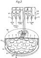
- PYROX Reactor is to be used, and such a reactor is shown diagrammatically in Figure 2.
- the PYROX Reactor which provides for batch processing of wafers, has a water cooled 102 reactor head 100 within which there is a rotatable circular table 101 upon which are placed wafers 103 to be treated.
- the table 101 which supports a graphite wafer carrier 104, is heated from underneath during processing, the temperature of the table 101 and hence of the wafers being measured by means of a thermocouple (not shown).
- 7.62cm (three inch) wafers were used.
- the wafers were held on silicon carbide coated graphite succeptors 99, arranged in a circle of twelve around the outer ring of an eighteen wafer carrier.
- the reactor head consists of four concentric zones which, moving out from the centre, are termed A, B, C, and D.
- the gas flow to each of these zones can be adjusted to vary the conditions within the reactor head.
- Separate flow control valves 105, 106 and 107 and pressure gauges 108, 109, and 110 are provided for zones A, B, and C; flow to Zone D is not independently controllable.
- the composition of the gas fed to the reactor head can be adjusted by flow control valves 111-116 in each of six flowlines, the flowrates in each of the flowlines being monitored by means of rotameters 117-122, containing floats 123-128.
- zone pressures were maintained at values routinely used when depositing USG or PSG: ZONE A 89.63 KPa (13 p.s.i.) ZONE B 75.84 KPa (11 p.s.i.) ZONE C 82.74 KPa (12 p.s.i.) ZONE D - not directly measurable.
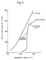
- the deposition rate is limited by the diffusion rate of the reactants through a very thin depleted zone near the surface which will follow the contours of the surface.
- the silane and oxygen system shows a very small dependence of deposition rate on temperature (in the example illustrated it is practically constant at 9 x 10 -10 ⁇ m (9A) per °C, which is small when compared to the 29 x 10 -10 ⁇ m (29A) per °C to 63 x 10 -10 ⁇ m (63A) per °C for the arsine-silane-oxygen example shown) and the lack of any diffusion limit indicates that it is a homogeneous gas phase reaction.
- the significance of the heterogeneous reaction is that the deposition rate is controlled by the surface temperature and not by the geometry of the surface, and hence one may expect such a reaction to give conformal oxide coatings.
- Figure 5 shows such a conformal coating 50 of ASG over a 1 ⁇ m high aluminium track 51 with near vertical side walls 52.
- Figure 6 shows a typical non-conformal coating 60 produced as a result of a homogenous reaction between silane and oxygen.
- the results of the homogeneous reaction can be seen as overhangs 61 at the sides of the track 51; such overhangs are typical of the non-conformal deposition which characterises homogeneous reactions.
- Zone pressures were maintained as above at 89.63KPa (13 psi) Zone A; 75.84KPa (11 psi) Zone B; 82.74KPa (12 psi) Zone C.
- Plate temperature 450°C. 7.62cm (3-inch) silicon wafers placed in outer circle of an 18 wafer plate.
- the As 2 O 3 content of the glasses produced under heterogeneous reaction conditions were as follows:
- the gettering process involves heating the device in an atmosphere of phosphorus oxychloride (POCl 3 ) and oxygen to produce a layer of phosphorus pentoxide P 2 O 5 about 0.4 ⁇ m (400A) thick on the entire surface of the slice.
- POCl 3 phosphorus oxychloride
- the P 2 O 5 layer acts as a doping source of phosphorus atoms which heavily dope the back of the slice (the PSG and SiO 2 layers protecting the front of the slice) when it is heated to about 1000°C.
- the first dielectric layer must be able to withstand the back gettering process.
- Evaluation of the thermal stability of the ASG layers produced according to the invention has shown that they are capable of undergoing the temperature cycling involved in back gettering without losing their integrity.
- a surprising and beneficial side effect of the back gettering process is that in the etching step following gettering the ASG tends to develop a smoother topography.
- the result is equivalent to that observed when PSG or ASG (which can be heat reflowed if it contains above about 7-10% As 2 O 3 ) is reflowed by heating.
- This smoothing effect is advantageous because although a conformal coating will be free from overhangs, it will have steep sided features which may cause some difficulty during metallisation or subsequently (although any such difficulties will tend to be minimal compared to those found with a non-conformal non-reflowed layer).
- the 'reflowed' type of topography is generally free of steep sided features and has low step angles, which minimise problems both during metallisation and in subsequent processing.
- the following mechanism is responsible for the smoothing effect during etching.
- phosphorus (as P 2 O 5 ) diffuses into the dielectric layer, the amount which diffuses at any point being dependent upon the topography at that point.
- the dielectric will have a large surface to volume ratio and the diffusing phosphorus atoms will tend to follow convergent paths.
- the dielectric will have a small surface to volume ratio and the diffusing phosphorus atoms will follow divergent paths.
- the dielectric will have a higher phosphorus content, while the concave parts will have a lower phosphorus content. Since the etch rate of ASG (and PSG) increases with increasing P 2 O 5 content (and As 2 O 3 content), the convex parts will etch faster than the concave parts, leading to a smoothing of the topography.
- ASG layers produced as above have been found to have advantages other than just the ability to form conformal coatings at relatively low temperatures. In particular, it has been found that the etch properties of ASG are superior to those of PSG.
- PSG is frequently used to form the first dielectric layer over the polysilicon gates and tracks of an integrated circuit, i.e., layer 4 over gates 3 of Figure 1.
- Beneath layer 4 and gates 3 is a layer 2 of SiO 2 produced by surface oxidation of the substrate 1.
- the etch rate of PSG is considerably greater than the etch rate of SiO 2 , and this means that undercutting of the window in the PSG layer is a problem.
- Figure 7a shows the structure at the start of etching, with the contact window positions marked by holes 20 in a mask 21 which has been deposited over the PSG layer 4. As the etch dissolves the PSG the contact window 22 grows laterally and vertically.
- Figure 7b which shows the situation at the instant that the etch has progressed vertically as far as the SiO 2 layer, it can be seen that the contact window 22 has spread widthwise dramatically to produce a very wide hole, the upper ends 23,23' of which extend far beyond the edges of the hole 20 in the mask.
- Figure 7c which shows the situation after the SiO 2 has been etched, it can be seen that there has been considerably more lateral spread.
- FIGs 7d and 7e show how the problem is currently dealt with.
- two etching steps are used to produce the contact windows.
- a first etch is used to reach the stage shown in Figure 7b, i.e., formation of the via hole in the PSG.
- the first etch is stopped there, the first mask removed, and a second mask 25 applied over the PSG, Figure 7d.
- This second mask 25 covers the sides of the via and protects the PSG from the second etch.
- the contact windows produced in this way have basal diameters of up to about 4.5 ⁇ m - 5 ⁇ m and are on the limit of what is acceptable for use with 3 ⁇ m track width geometry. It would be very desirable to be able to produce contact windows smaller than this. It would also be very desirable to produce contact windows without having to use a mask-etch-mask-etch process.
- Figure 8a shows a device similar to that of Figure 7a except that the PSG layer 4 has been replaced by an ASG layer 44. It has been found that the etch rate of ASG (at least for ASG deposited accordinging to the invention) is very similar to that of SiO 2 layer 2. It is therefore possible to etch contact windows in a single etch step without serious undercutting. From Figure 8b it can be seen that the contact window has only spread very slightly compared with Figure 7c.
- FIG. 9a is an SEM photograph of such a contact window. It can be seen from figures 8b and 9a that the contact window has a steeper slope (60 in Figure 9a) in a region towards its upper edge. This slope is the result of the arsenic depleted surface region (produced during the above-mentioned back gettering process) etching more slowly than the bulk of the ASG. It has been found that this feature defines the window size more closely.
- Figure 9b is an SEM photograph of a contact window produced as above which has been etched to remove the P 2 O 5 layer produced during the back gettering process. It can be seen that the edge profile of the contact window has been evened out. It has been found that metallisation of contact windows produced as above is particularly easy.
Landscapes
- Formation Of Insulating Films (AREA)
- Internal Circuitry In Semiconductor Integrated Circuit Devices (AREA)
- Thin Film Transistor (AREA)
- Semiconductor Integrated Circuits (AREA)
- Insulated Gate Type Field-Effect Transistor (AREA)
- Mechanical Treatment Of Semiconductor (AREA)
- Element Separation (AREA)
- Crystals, And After-Treatments Of Crystals (AREA)
Abstract
Description
- This invention relates to semiconductor devices and to methods of fabricating them.
- In the manufacture of integrated circuits and other semiconductors devices it is necessary to provide dielectric layers between the various conducting layers. In a typical integrated circuit, such as that shown in section in Figure 1, there will be several dielectric layers, each of which may have a different composition. In the Figure, a
silicon substrate 1 has been surface oxidised to provide a silicon dioxide (dielectric)layer 2 upon which polysilicon gates and interconnects 3 are produced. The first dielectric layer ofinterest 4 insulates the polysilicon features from subsequent features except at the points (contact windows) 9,9' where it is removed to provide contact with ametallisation layer 5 which is next to be deposited. Following definition of the metallisation pattern, a second dielectric layer may be the final layer or, as in the example shown, may he followed by afurther metallisation layer 7 interconnected with the first 5 by means ofcontact windows 9" (usually referred to as vias in this position) as before. Following the last metallisation layer, a finaldielectric layer 8 may be deposited and this serves to prevent the ingress of water and other contaminants and also resists surface scratching. - The compositions of the dielectric layers, particularly
layers Layer 4 is generally a phosphorus doped silicon dioxide glass (PSG) film, but may be an undoped silicon dioxide glass (USG) film. These glass films, which are usually applied by chemical vapour deposition (CVD), are widely used in the microelectronics industry as dielectric layers between different conductor levels. Unfortunately, most of the glass deposition processes suffer from poor step coverage; that is, they provide poor coverage of vertical topographical features (such as gates and tracks etc.). This problem of step coverage is dealt with at length in the paper "The step coverage of undoped and phosphorus-doped SiO2 glass films" by R. M. Levin and K. Evans Lutterodt, J. Vac. Sol. Technol. BI(1), Jan-Mar 1983 p.54. - The basis for the CVD glass deposition processes is the reaction of silane and oxygen:-

- This is a homogeneous gas phase reaction: the product is formed in the gas phase and then condenses on any adjacent surface. The tendency is for the sides of any step to be sheltered by the upper part of the step and hence the product grows more rapidly on the upper part of the step. Lateral growth from the top corners of the step will screen the areas beneath it and thus the overhang will be self-perpetuating. If a metallisation layer is subsequently deposited onto the feature, the layer may become discontinuous below the overhang.
- The problem of poor step coverage may be alleviated if phosphine gas is added to the reactants. Phosphine does not change the deposition mechanism, but it does add a few percent of phosphorus pentoxide to the silicon dioxide layer converting it to a phosphosilicate glass (PSG). This PSG has some advantages over USG:
- (i) It melts at lower temperatures compatible with semiconductor processing, and if heated to about 1000°C the glass will flow and surface tension will even out the overhang and the re-entrant to give smooth coverage;
- (ii) the intrinsic stress in the film is lower;
- (iii) the phosphorous atoms will getter any alkali ions that might otherwise penetrate the film.
- PSG is, however, not suitable for use as the second dielectric layer 6: the
metallisation 5 is generally aluminium, and as can be seen from the figure it is in contact with elemental silicon in thecontact windows 9,9'; if the slice temperature is raised beyond about 570°C, an aluminium/silicon eutectic (M.P. 577°C) will be formed with the resultant destruction of the device. This effect limits the deposition temperatures and subsequent processing temperatures fordielectric layers Dielectric layers - Alternative reactions have been used in an effort to produce conformal coatings (which do not need heat treatment after deposition to give a satisfactory surface) of silicon dioxide. Conformal coatings can be expected if homogeneous gas phase reactions are eliminated, and this is achieved in the following two reaction systems:


- Both of these systems give conformal coatings, but as they are more stable the reactions only occur in the temperature range 650 to 950°C. This temperature can be reduced somewhat by introducing some of the energy required by means of a gas phase plasma. Unfortunately the equipment to produce suitable plasmas is very expensive and, furthermore, the plasma may introduce some electrical instabilities into any device produced in this way.
- It can be seen from the above that there exists a need for a method of producing a conformal dielectric coating which can be carried out below 550°C, and preferably below 500°C, and which does not require the use of plasma equipment.
- The present invention is based on our surprising discovery that it is possible to modify the silane/oxygen reaction by inhibiting the homogeneous gas phase reactions so that only the heterogeneous surface reactions occur, such that the resulting silicon dioxide based coatings are conformal and do not require heat treatment before metallisation, the reaction proceeding at temperatures below 500°C, without the use of a plasma.
- The concept of inhibiting the gas phase reactions of a silane-oxygen mixture is not in itself new; the subject was first extensively investigated by H. J. Emeleus and K. Stewart in their paper "The oxidation of silicon hydrides" in J.Chem.Soc., p.1182 (1935). In this paper they reported their study of the gas phase kinetics in which they found that several substances would inhibit the gas phase reactions; of the substances studied, ethylene was the most effective.
- Middelhoek and Klinkhamer (fifth international conference of the Electrochemical Society, 1975, pp. 19-29) used the results obtained by Emeleus and Stewart and tried to inhibit the homogeneous reactions with ethylene. In their paper they indicate that ethylene is useful as an inhibitor of the homogeneous gas phase reactions.
- However, in a more recent paper - RCA Review, Vol.37, No.1, March 1976, p.3 - p.54 - Kern, Schnable, and Fisher report that ethylene is effective as a selective inhibitant of the homogeneous reaction only at very low O2:SiH4 ratios - at ratios which they consider to be not normally usable for film deposition. Experiments (the results of which were confirmed in a private communication from Middelhoek to Kern) by Kern et al show that, at O2:SiH4 ratios more suited to film deposition; ethylene does not act as a selective inhibitant.
- It is clear from the paper of Kern et al that selective suppression of the homogeneous reaction would be desirable to improve the quality of USG and PSG layers; however, no such suppressant is proposed.
- We have made the surprising discovery that arsine acts much more effectively as an inhibitor in the silane-oxygen reaction than does ethylene, and that it is possible to produce a silicon dioxide-based arsenosilicate glass as a conformal coating.
- Arsenosilicate glasses have found limited use in semiconductor device manufacture, but such use has principally been restricted to use as dopant sources. A typical example of such use can be found in PCT patent application no. WO 82/01380 of the NCR corporation, entitled "Process for forming a polysilicon gate integrated circuit device". In the NCR application an ASG layer is prepared by applying a solution of an arsenic-doped polymer in alcohol to the device, followed by spin coating to produce a uniform layer. The device is then baked to drive off the solvents to leave the ASG. This ASG layer is then photolithographically masked and etched to produce a masking layer for use during p-type doping. Subsequently the ASG mask acts as a doping source of n-type atoms.
- Arsenic ions diffuse from the ASG layer (mask) into underlying silicon and polysilicon layers during a high temperature baking step to produce n+ regions. Subsequently the ASG layer (mask) is completely removed by etching in hydrofluoric acid. The remaining processing steps, forming an oxide layer, vias, a metallisation layer, and a passivation layer, are conventional and of no interest here.
- It can be seen that the NCR application, which concerns the use of an ASG layer as a combined mask and dopant source and which is to be removed before the device fabrication is complete, is very different to the present invention and is intended to solve problems which are very different to those to which the present invention is directed.
- An exception to the general use of ASG as a dopant source is disclosed in US patent 4,355,454 of Tasch et al which details use of an arsenic-doped glass as an insulating layer over polysilicon gates and interconnects. The ASG is deposited at about 500 degrees C using silane, oxygen and arsine. After the arsenic doped layer is deposited it is heated to about 850 to 900 degrees C to reflow the layer and give the surface of the slice a smoother topology. In devices having multilevel interconnects of polysilicon, as with those having only single level interconnects of polysilicon, the ASG is only deposited after the last layer of polysilicon has been deposited.
- It is clear that Tasch et al failed to appreciate that it is possible to use arsine to control the silane oxygen reaction to produce conformal coatings of ASG. Nowhere is the reaction type referred to, and no mention is made of conformality - a property which would certainly have been mentioned if Tasch et al had produced it. In the processes described and claimed, the ASG is heated to reflow it; a step which would be unnecessary if the layer was conformal. Since reflowing involves heating to 850-900°C, it is clear that such a process cannot be used to deposit arsenic-doped glass over metallisation layers.
- According to a first aspect of the present invention, in a reaction of a mixture comprising silane oxygen and arsenic in a chemical vapour deposition process without plasma assistance to produce an arsenosilicate glass on a substrate, the use of arsine in a sufficient concentration and of reaction conditions, such as homogeneous gas phase reactions between silane and oxygen are inhibited, so that the arsenosilicate glass is produced as a conformal coating on the substrate.
- Preferably, the reaction is carried out at a temperature below 500°C.
- Preferably, the volume ratio of silane to arsine lies in the range 3.8: to 11. 7: 1, with the volume ratio of oxygen to silane in the
range 18. 5: 1 to 41:1. - According to a second aspect of the present invention, there is provided a method of producing an arsenosilicate glass in a chemical vapour deposition process without plasma-assistance, the method involving the reaction of a reactant mixture of silane, oxygen and arsine, characterised in that the reaction takes place in the presence of a diluent gas, and in that the reaction conditions and the composition of the reactant mixture are selected such that the arsenosilicate glass is produced as a conformal coating as the result of a predominantly heterogeneous reaction, and that the reactor type and the reaction conditions are such that in the absence of arsine the reaction between silane and oxygen is predominantly homogeneous.
- According to the third aspect of the present invention, there is provided a method of producing a conformal arsenosilicate glass coating in a chemical vapour deposition process involving reactions between silane and oxygen without plasma-assistance, the reaction mixture including arsine, wherein the reactions between silane and oxygen are predominantly of a heterogeneous nature, this being achieved via selection of the gas concentrations to lie in the ranges such that the volume ratio of silane to arsine is between 3.8 to 1 and 11.7 to 1 and the volume ratio of oxygen to silane is between 18.5 to 1 and 41 to 1, and wherein the reactor type and the reaction conditions are such that in the absence of arsine the reaction between silane and oxygen is predominately homogeneous.
- The invention will now be further described by way of example only with reference to the accompanying drawings in which:
- Figure 1 shows a vertical section through a multi level integrated circuit device;
- Figure 2 is a diagrammatic representation of the apparatus used in the present invention;
- Figure 3 is a graph showing how changes in the arsine-silane flow-rate affect the deposition rate with temperature;
- Figure 4 is a graph of deposition rate against temperature for the silane-oxygen system and the silane-arsine-oxygen system;
- Figure 5 is an SEM photograph showing a step covered by a conformal coating produced according to the invention;
- Figure 6 is an SEM photograph showing poor step coverage;
- Figure 7 shows the via formation process with PSG;
- Figure 8 shows the via formation process with ASG produced according to the invention;
- Figure 9 is an SEM photograph showing contact windows produced in ASG according to the invention.
- As has been previously explained, Figure 1 is a vertical section through a typical multi-level integrated circuit. In known devices
dielectric layers layer 4 may be PSG and layers 6 and 8 plasma deposited silicon dioxide or silicon nitride. In devices according to the invention, any or all oflayers - The ASG is produced in a chemical vapour deposition (CVD) process such as may be carried out in a commercial CVD machine. Machines designed for the silane-oxygen reaction for CVD of silicon dioxide, such as the PYROX Reactor produced by Tempress-Unicorp, are particularly suitable for carrying out the ASG deposition, although other machines may also be suitable. For the purposes of description it will be assumed that a PYROX Reactor is to be used, and such a reactor is shown diagrammatically in Figure 2.
- The PYROX Reactor, which provides for batch processing of wafers, has a water cooled 102
reactor head 100 within which there is a rotatable circular table 101 upon which are placedwafers 103 to be treated. The table 101, which supports agraphite wafer carrier 104, is heated from underneath during processing, the temperature of the table 101 and hence of the wafers being measured by means of a thermocouple (not shown). In the experiments to be reported, 7.62cm (three inch) wafers were used. The wafers were held on silicon carbide coatedgraphite succeptors 99, arranged in a circle of twelve around the outer ring of an eighteen wafer carrier. - The reactor head consists of four concentric zones which, moving out from the centre, are termed A, B, C, and D. The gas flow to each of these zones can be adjusted to vary the conditions within the reactor head. Separate
flow control valves pressure gauges Flowline Identity Gas Composition Rotameter Porter Model Number Float Type Main N2 B250-8 Stainless Steel Nitrogen Silane 5%SiH4 in N2 B125-40 Stainless Steel Dopant 1 1%AsH3 in N2 B125-40 Stainless Steel Oxygen O2 B125-40 Stainless Steel Dilution Nitrogen N2 B250-8 Stainless Steel - Throughout the experiments the zone pressures were maintained at values routinely used when depositing USG or PSG:
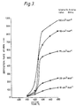
ZONE A 89.63 KPa (13 p.s.i.) ZONE B 75.84 KPa (11 p.s.i.) ZONE C 82.74 KPa (12 p.s.i.) ZONE D - not directly measurable. - Results for reactions carried out at plate (wafer) temperatures between 400 and 450 degrees C. are shown in Figure 3. This figure shows how temperature affects the thin film deposition rate for five different total hydride flow rates (19,29,75,110,130 cc/minute) with the oxygen flow rate held constant at 2500 cc/minute, and with the main nitrogen and dilution nitrogen flow rates each held at 38 litres/minute.
- It is instructive to compare the deposition vs. temperature curves obtained with silane-arsine-oxygen with those obtained with the silane-oxygen system. In Figure 4 examples of each are compared. The curve for silane-arsine-oxygen (for 75cc total hydride flow, SiH4: Arsine ratio = 61:14) shows the two regions which characterise it as a heterogeneous reaction. In the low temperature region, where there is kinetic control, the deposition rate shows the exponential rise with temperature predicted by the Arrhenius rate equation:-

conformal coating 50 of ASG over a 1µmhigh aluminium track 51 with nearvertical side walls 52. This should be compared with Figure 6 which shows a typicalnon-conformal coating 60 produced as a result of a homogenous reaction between silane and oxygen. The results of the homogeneous reaction can be seen asoverhangs 61 at the sides of thetrack 51; such overhangs are typical of the non-conformal deposition which characterises homogeneous reactions. - The conformal coating of ASG as shown in Figure 5 was produced with the instrument settings given in the following example:
-
Gas Rotameter reading height in mm Main N2 56 5% SiH4inN2 40 1% AsH3inN2 44 Dilution N2 56 Oxygen 95 - 61 cc/minute of pure SiH4
- 14 cc/minute of pure AsH3
- 2500 cc/minute of pure O2
- The zone pressures were maintained as above at 89.63KPa (13 psi) Zone A; 75.84KPa (11 psi) Zone B; 82.74KPa (12 psi) Zone C. Plate temperature = 450°C. 7.62cm (3-inch) silicon wafers placed in outer circle of an 18 wafer plate.
- Thin film deposition of rate of ASG = 0.575µm (575A)/minute. Glass deposited under these conditions was found to have an intrinsic stress of 5kNcm-2
(5 x 10⁸Dynes cm-2) tensile.
The glass had a composition of 12 mole% As2O3,
88 mole% SiO2. - Satisfactory conformal coatings have been produced with silane:arsine ratios between about 3.8:1 and 11.7:1. A deposition rate versus temperature curve for a silane flow rate of 60cc minute-1 and an arsine flow rate of 10cc min-1 (with 2500cc min-1O2, main N2 = 38 Litres min-1, and dilution N2 = 38 Litres min-1) is shown in Figure 3a.
- It has been found that in general an increase in oxygen and/or silane concentration favours a homogeneous reaction and an increase in arsine concentration favours heterogeneous reaction.
- The following gas mixtures, used under the conditions set out above, have been found to give the reaction type indicated:
Run Arsine ml/min Silane ml/min Oxygen ml/min Nitrogen ml/min Reaction A 6.5 61 1.4 76 heterogeneous B 3.1 61 1.4 76 homogeneous C 6.5 76 1.4 76 heterogeneous D 6.5 113 1.4 76 homogeneous E 6.5 148 1.4 76 homogeneous - The As2O3 content of the glasses produced under heterogeneous reaction conditions were as follows:
- Run A 6% at 400°C, 4% at 450°C
- Run C 3% at 400°C, 2% at 450°C.
- It is usual after producing the first
dielectric layer 2, and before producing thecontact windows dielectric layer 2 is of PSG, the gettering process involves heating the device in an atmosphere of phosphorus oxychloride (POCl3) and oxygen to produce a layer of phosphorus pentoxide P2O5 about 0.4 µm (400A) thick on the entire surface of the slice. The P2O5 layer acts as a doping source of phosphorus atoms which heavily dope the back of the slice (the PSG and SiO2 layers protecting the front of the slice) when it is heated to about 1000°C. This heavy doping damages the silicon lattice of the slice to form sites which act as traps for the unwanted ions which are mobile at this temperature. When the slice is cooled the unwanted ions are trapped in the sites to which they migrated during the heating step, which (because of the effects of the PSG and SiO2 layers) are to the rear of the slice, well away from the front of the slice where the active regions are to be formed. The P2O5 layer is removed by etching in dilute HF after formation of the contact windows. - As this gettering step is normally an essential step in device manufacture, the first dielectric layer must be able to withstand the back gettering process. Evaluation of the thermal stability of the ASG layers produced according to the invention has shown that they are capable of undergoing the temperature cycling involved in back gettering without losing their integrity.
- A surprising and beneficial side effect of the back gettering process is that in the etching step following gettering the ASG tends to develop a smoother topography. The result is equivalent to that observed when PSG or ASG (which can be heat reflowed if it contains above about 7-10% As2O3) is reflowed by heating. This smoothing effect is advantageous because although a conformal coating will be free from overhangs, it will have steep sided features which may cause some difficulty during metallisation or subsequently (although any such difficulties will tend to be minimal compared to those found with a non-conformal non-reflowed layer). The 'reflowed' type of topography is generally free of steep sided features and has low step angles, which minimise problems both during metallisation and in subsequent processing.
- It is believed that the following mechanism is responsible for the smoothing effect during etching. When the wafer is heated in the POCl3 atmosphere for back gettering, phosphorus (as P2O5) diffuses into the dielectric layer, the amount which diffuses at any point being dependent upon the topography at that point. Where the surface of the wafer is convex, such as at the top corner of a step, the dielectric will have a large surface to volume ratio and the diffusing phosphorus atoms will tend to follow convergent paths. Conversely, where the wafer is concave, such as at the foot of a step, the dielectric will have a small surface to volume ratio and the diffusing phosphorus atoms will follow divergent paths. Consequently where the wafer is convex the dielectric will have a higher phosphorus content, while the concave parts will have a lower phosphorus content. Since the etch rate of ASG (and PSG) increases with increasing P2O5 content (and As2O3 content), the convex parts will etch faster than the concave parts, leading to a smoothing of the topography.
- One further change noticed as a result of back gettering when using an ASG dielectric is that there is a depletion of the arsenic content in the surface region of the layer.
- ASG layers produced as above have been found to have advantages other than just the ability to form conformal coatings at relatively low temperatures. In particular, it has been found that the etch properties of ASG are superior to those of PSG.
- PSG is frequently used to form the first dielectric layer over the polysilicon gates and tracks of an integrated circuit, i.e.,
layer 4 over gates 3 of Figure 1. Beneathlayer 4 and gates 3 is alayer 2 of SiO2 produced by surface oxidation of thesubstrate 1. When it is desired to form contact windows to the underlying silicon, as at 9' in Figure 1, it is necessary to etch both the PSG and the SiO2. Unfortunately, the etch rate of PSG is considerably greater than the etch rate of SiO2, and this means that undercutting of the window in the PSG layer is a problem. - This is illustrated in Figure 7. Figure 7a shows the structure at the start of etching, with the contact window positions marked by
holes 20 in amask 21 which has been deposited over thePSG layer 4. As the etch dissolves the PSG thecontact window 22 grows laterally and vertically. In Figure 7b, which shows the situation at the instant that the etch has progressed vertically as far as the SiO2layer, it can be seen that thecontact window 22 has spread widthwise dramatically to produce a very wide hole, the upper ends 23,23' of which extend far beyond the edges of thehole 20 in the mask. In Figure 7c which shows the situation after the SiO2has been etched, it can be seen that there has been considerably more lateral spread. Such a contact window is unacceptable for high density circuits as it would require the use of unacceptably wide tracks and interconnects. Figures 7d and 7e show how the problem is currently dealt with. In this process two etching steps are used to produce the contact windows. A first etch is used to reach the stage shown in Figure 7b, i.e., formation of the via hole in the PSG. The first etch is stopped there, the first mask removed, and asecond mask 25 applied over the PSG, Figure 7d. Thissecond mask 25 covers the sides of the via and protects the PSG from the second etch. - Following application of the
second mask 25, the second etch is carried out; the resulting contact window is shown in Figure 7e. This contact window, although not ideal, has very much less lateral spread than that shown in Figure 7c, and is adequate for current high density circuits. - The contact windows produced in this way have basal diameters of up to about 4.5 µm - 5 µm and are on the limit of what is acceptable for use with 3 µm track width geometry. It would be very desirable to be able to produce contact windows smaller than this. It would also be very desirable to produce contact windows without having to use a mask-etch-mask-etch process.
- Figure 8a shows a device similar to that of Figure 7a except that the
PSG layer 4 has been replaced by an ASG layer 44. It has been found that the etch rate of ASG (at least for ASG deposited acording to the invention) is very similar to that of SiO2 layer 2. It is therefore possible to etch contact windows in a single etch step without serious undercutting. From Figure 8b it can be seen that the contact window has only spread very slightly compared with Figure 7c. - Contact windows produced in this way have been found to possess not only a good shape, but they are also generally of smaller size than those produced with PSG. Basal diameters have been of the order of 3.6-3.7 µm for windows produced in this single step process. Figure 9a is an SEM photograph of such a contact window. It can be seen from figures 8b and 9a that the contact window has a steeper slope (60 in Figure 9a) in a region towards its upper edge. This slope is the result of the arsenic depleted surface region (produced during the above-mentioned back gettering process) etching more slowly than the bulk of the ASG. It has been found that this feature defines the window size more closely.
- Figure 9b is an SEM photograph of a contact window produced as above which has been etched to remove the P2O5 layer produced during the back gettering process. It can be seen that the edge profile of the contact window has been evened out. It has been found that metallisation of contact windows produced as above is particularly easy.
- Although the invention has been described in relation to use on silicon wafers, its use is by no means limited to silicon - for example it should also find application on gallium arsenide, indium phosphide and other semiconductor materials.
- Devices made using ASG as sub-metal dielectric have been found to have performance much the same as that found with equivalent devices made using PSG.
- Using ASG over ASG instead of polyimide over PSG or plasma oxide over PSG appears to give dramatically improved reliability. In routine accelerated ageing tests carried out at 85°C in 85% R.H. unprotected ASG over ASG chips showed no deterioration after 1000 hours. Equivalent constructions using polyimide over PSG last only 40 to 120 hours, as do devices using plasma oxide over PSG.
Claims (14)
- In a reaction of a mixture comprising silane, oxygen and arsine in a chemical vapour deposition process without plasma assistance to produce an arsenosilicate glass on a substrate, the use of arsine in a sufficient concentration and at reaction conditions, such that homogeneous gas phase reactions between silane and oxygen are inhibited, so that the arsenosilicate glass is produced as a conformal coating on the substrate.
- A method of producing an arsenosilicate glass in a chemical vapour deposition process without plasma-assistance, the method involving the reaction of a reactant mixture of silane, oxygen and arsine, characterised in that the reaction takes place in the presence of a diluent gas, and in that the reaction conditions and the composition of the reactant mixture are selected such that the arsenosilicate glass is produced as a conformal coating as the result of a predominantly heterogeneous reaction and that the reactor type and the reaction conditions are such that in the absence of arsine the reaction between silane and oxygen is predominantly homogeneous.
- A method as claimed in claim 2, wherein the volume ratio of silane to arsine lies in the range 3. 8 : 1 to 11.7 : 1, with the volume ratio of oxygen to silane in the range 18.5 : 1 to 106 : 1.
- A method of producing a conformal arsenosilicate glass coating in a chemical vapour deposition process involving reactions between silane and oxygen without plasma-assistance, the reaction mixture including arsine, wherein the reactions between silane and oxygen are predominantly of a heterogeneous nature, this being achieved via selection of the gas concentrations to lie in the ranges such that the volume ratio of silane to arsine is between 3.8 to 1 and 11.7 to 1 and the volume ratio of oxygen to silane is between 18.5 to 1 and 41 to 1 and wherein the reactor type and the reaction conditions are such that in the absence of arsine the reaction between silane and oxygen is predominately homogeneous.
- A method as claimed in any one of claims 2 to 4, wherein the reaction is carried out at a temperature below 500°.
- A method as claimed in claim 3, wherein the reaction is carried out at a temperature between 400°C and 550°C.
- A method of fabricating a semiconductor device, the method including the step of producing a layer of arsenosilicate glass as a conformal coating according to the method of any one of claims 2 to 6.
- A method as claimed in claim 7, wherein the semiconductor device is formed on a silicon substrate.
- A method as claimed in claim 7 or claim 8, wherein the arsenosilicate glass layer lies over a metallisation layer.
- A method as claimed in claim 9, wherein the metallisation layer comprises aluminium.
- A method as claimed in claim 9 or claim 10, wherein the metallisation layer is in physical contact with a semiconductor region of the device.
- A method as claimed in any one of claims 7 to 11, the method further comprising the step of depositing a metallisation layer over the arsenosilicate glass.
- A method as claimed in claim 12, the method further comprising the step of depositing an additional layer of arsenosilicate glass over the metallisation layer recited in claim 12.
- A method as claimed in claim 12 or claim 13, wherein the metallisation layer recited in claim 12 comprises aluminium.
Applications Claiming Priority (2)
| Application Number | Priority Date | Filing Date | Title |
|---|---|---|---|
| GB848401250A GB8401250D0 (en) | 1984-01-18 | 1984-01-18 | Semiconductor fabrication |
| GB8401250 | 1984-01-18 |
Publications (3)
| Publication Number | Publication Date |
|---|---|
| EP0150088A2 EP0150088A2 (en) | 1985-07-31 |
| EP0150088A3 EP0150088A3 (en) | 1985-08-28 |
| EP0150088B1 true EP0150088B1 (en) | 1996-10-16 |
Family
ID=10555133
Family Applications (1)
| Application Number | Title | Priority Date | Filing Date |
|---|---|---|---|
| EP85300172A Expired - Lifetime EP0150088B1 (en) | 1984-01-18 | 1985-01-10 | A semiconductor device comprising a dielectric layer |
Country Status (8)
| Country | Link |
|---|---|
| US (2) | US4731346A (en) |
| EP (1) | EP0150088B1 (en) |
| JP (1) | JPH079903B2 (en) |
| AT (1) | ATE144350T1 (en) |
| CA (1) | CA1266805A (en) |
| DE (1) | DE3588127T2 (en) |
| GB (1) | GB8401250D0 (en) |
| IE (1) | IE56660B1 (en) |
Families Citing this family (13)
| Publication number | Priority date | Publication date | Assignee | Title |
|---|---|---|---|---|
| JP2623812B2 (en) * | 1989-01-25 | 1997-06-25 | 日本電気株式会社 | Method for manufacturing semiconductor device |
| US5034801A (en) * | 1989-07-31 | 1991-07-23 | W. L. Gore & Associates, Inc. | Intergrated circuit element having a planar, solvent-free dielectric layer |
| US5285102A (en) * | 1991-07-25 | 1994-02-08 | Texas Instruments Incorporated | Method of forming a planarized insulation layer |
| EP0562625B1 (en) * | 1992-03-27 | 1997-06-04 | Matsushita Electric Industrial Co., Ltd. | A semiconductor device and process |
| EP0564136B1 (en) * | 1992-03-31 | 1998-06-03 | STMicroelectronics, Inc. | Method for planarization of an integrated circuit |
| US5500557A (en) * | 1992-04-30 | 1996-03-19 | Sgs-Thomson Microelectronics, Inc. | Structure and method for fabricating integrated circuits |
| US5479042A (en) * | 1993-02-01 | 1995-12-26 | Brooktree Corporation | Micromachined relay and method of forming the relay |
| JP2934565B2 (en) * | 1993-05-21 | 1999-08-16 | 三菱電機株式会社 | Semiconductor manufacturing apparatus and semiconductor manufacturing method |
| JPH0845936A (en) * | 1994-05-31 | 1996-02-16 | Texas Instr Inc <Ti> | High speed LSI semiconductor device using dummy leads and reliability improving method thereof |
| US5559052A (en) * | 1994-12-29 | 1996-09-24 | Lucent Technologies Inc. | Integrated circuit fabrication with interlevel dielectric |
| US5817571A (en) * | 1996-06-10 | 1998-10-06 | Taiwan Semiconductor Manufacturing Company, Ltd. | Multilayer interlevel dielectrics using phosphorus-doped glass |
| US6194301B1 (en) | 1999-07-12 | 2001-02-27 | International Business Machines Corporation | Method of fabricating an integrated circuit of logic and memory using damascene gate structure |
| US7270940B2 (en) * | 2002-12-18 | 2007-09-18 | International Business Machines Corporation | Method of structuring of a substrate |
Family Cites Families (12)
| Publication number | Priority date | Publication date | Assignee | Title |
|---|---|---|---|---|
| US3925572A (en) * | 1972-10-12 | 1975-12-09 | Ncr Co | Multilevel conductor structure and method |
| JPS6032974B2 (en) * | 1977-03-16 | 1985-07-31 | 株式会社日立製作所 | Manufacturing method of semiconductor device |
| JPS5534444A (en) * | 1978-08-31 | 1980-03-11 | Fujitsu Ltd | Preparation of semiconductor device |
| JPS5544713A (en) * | 1978-09-26 | 1980-03-29 | Toshiba Corp | Semiconductor device |
| DE2936724A1 (en) * | 1978-09-11 | 1980-03-20 | Tokyo Shibaura Electric Co | Semiconductor device contg. layer of polycrystalline silicon |
| US4319260A (en) * | 1979-09-05 | 1982-03-09 | Texas Instruments Incorporated | Multilevel interconnect system for high density silicon gate field effect transistors |
| US4355454A (en) * | 1979-09-05 | 1982-10-26 | Texas Instruments Incorporated | Coating device with As2 -O3 -SiO2 |
| JPS56150830A (en) * | 1980-04-25 | 1981-11-21 | Hitachi Ltd | Semiconductor device |
| JPS59174544A (en) * | 1983-03-25 | 1984-10-03 | Nippon Electric Glass Co Ltd | Glass for coating semiconductor |
| JPH0630355B2 (en) * | 1983-05-16 | 1994-04-20 | ソニー株式会社 | Semiconductor device |
| US4535528A (en) * | 1983-12-02 | 1985-08-20 | Hewlett-Packard Company | Method for improving reflow of phosphosilicate glass by arsenic implantation |
| US4548671A (en) * | 1984-07-23 | 1985-10-22 | Rca Corporation | Method of making a charge-coupled device imager which includes an array of Schottky-barrier detectors |
-
1984
- 1984-01-18 GB GB848401250A patent/GB8401250D0/en active Pending
-
1985
- 1985-01-10 EP EP85300172A patent/EP0150088B1/en not_active Expired - Lifetime
- 1985-01-10 AT AT85300172T patent/ATE144350T1/en not_active IP Right Cessation
- 1985-01-10 DE DE3588127T patent/DE3588127T2/en not_active Expired - Fee Related
- 1985-01-11 CA CA000471951A patent/CA1266805A/en not_active Expired - Lifetime
- 1985-01-16 US US06/691,819 patent/US4731346A/en not_active Expired - Lifetime
- 1985-01-17 IE IE104/85A patent/IE56660B1/en not_active IP Right Cessation
- 1985-01-18 JP JP60007309A patent/JPH079903B2/en not_active Expired - Lifetime
-
1990
- 1990-09-12 US US07/582,114 patent/US5130782A/en not_active Expired - Fee Related
Non-Patent Citations (2)
| Title |
|---|
| Microelectronic Materials, C.R.M. Grosvenor, pages 158-162 and 302-307 (1989) * |
| Solid State Technology, L.W. Winkle and C.W. Nelson pages 123-128 (1981) * |
Also Published As
| Publication number | Publication date |
|---|---|
| GB8401250D0 (en) | 1984-02-22 |
| ATE144350T1 (en) | 1996-11-15 |
| CA1266805A (en) | 1990-03-20 |
| JPS60246642A (en) | 1985-12-06 |
| EP0150088A3 (en) | 1985-08-28 |
| DE3588127D1 (en) | 1996-11-21 |
| DE3588127T2 (en) | 1997-02-27 |
| IE56660B1 (en) | 1991-10-23 |
| US4731346A (en) | 1988-03-15 |
| US5130782A (en) | 1992-07-14 |
| EP0150088A2 (en) | 1985-07-31 |
| IE850104L (en) | 1985-07-18 |
| JPH079903B2 (en) | 1995-02-01 |
Similar Documents
| Publication | Publication Date | Title |
|---|---|---|
| EP0440154B1 (en) | Two step process for forming an oxide layer over a stepped surface of a semiconductor wafer | |
| US6306772B1 (en) | Deep trench bottle-shaped etching using Cl2 gas | |
| US5656556A (en) | Method for fabricating planarized borophosphosilicate glass films having low anneal temperatures | |
| US5166101A (en) | Method for forming a boron phosphorus silicate glass composite layer on a semiconductor wafer | |
| US4731346A (en) | Heterogeneous conformal CVD of arsenosilicate glass | |
| JP2710551B2 (en) | Plasma CVD process for forming low temperature flow BPSG | |
| US4557950A (en) | Process for deposition of borophosphosilicate glass | |
| EP0421203B1 (en) | An integrated circuit structure with a boron phosphorus silicate glass composite layer on semiconductor wafer and improved method for forming same | |
| EP0562625B1 (en) | A semiconductor device and process | |
| US4417914A (en) | Method for forming a low temperature binary glass | |
| JP2859864B2 (en) | Method for planarizing BPSG film surface | |
| US4630343A (en) | Product for making isolated semiconductor structure | |
| US6159870A (en) | Borophosphosilicate glass incorporated with fluorine for low thermal budget gap fill | |
| US6218319B1 (en) | Method of forming an arsenic silicon glass film onto a silicon structure | |
| US6387799B1 (en) | Method for fabricating titanium silicide film | |
| US6784117B2 (en) | Method for manufacturing a semiconductor device | |
| JP4160317B2 (en) | Insulating film manufacturing method and semiconductor device manufacturing method | |
| EP0060783A1 (en) | Process of forming a thin glass film on a semiconductor substrate | |
| JPH0778991A (en) | Semiconductor device and method of manufacturing semiconductor device | |
| JPH0379060A (en) | Manufacturing method for semiconductor integration circuit element | |
| EP0977249A2 (en) | An improved method of forming an arsenic silicon glass film onto a silicon structure | |
| JPH0379031A (en) | semiconductor equipment | |
| JPH03114231A (en) | Manufacture of semiconductor device | |
| JPS63196041A (en) | Formation of fine element | |
| JPS61212025A (en) | Forming method for phosphorus silicate glass (psg) film |
Legal Events
| Date | Code | Title | Description |
|---|---|---|---|
| PUAI | Public reference made under article 153(3) epc to a published international application that has entered the european phase |
Free format text: ORIGINAL CODE: 0009012 |
|
| PUAL | Search report despatched |
Free format text: ORIGINAL CODE: 0009013 |
|
| AK | Designated contracting states |
Designated state(s): AT BE CH DE FR GB IT LI LU NL SE |
|
| RTI1 | Title (correction) | ||
| AK | Designated contracting states |
Designated state(s): AT BE CH DE FR GB IT LI LU NL SE |
|
| 17P | Request for examination filed |
Effective date: 19851008 |
|
| 17Q | First examination report despatched |
Effective date: 19880728 |
|
| RAP3 | Party data changed (applicant data changed or rights of an application transferred) |
Owner name: BRITISH TELECOMMUNICATIONS PUBLIC LIMITED COMPANY |
|
| GRAG | Despatch of communication of intention to grant |
Free format text: ORIGINAL CODE: EPIDOS AGRA |
|
| GRAH | Despatch of communication of intention to grant a patent |
Free format text: ORIGINAL CODE: EPIDOS IGRA |
|
| GRAH | Despatch of communication of intention to grant a patent |
Free format text: ORIGINAL CODE: EPIDOS IGRA |
|
| GRAA | (expected) grant |
Free format text: ORIGINAL CODE: 0009210 |
|
| AK | Designated contracting states |
Kind code of ref document: B1 Designated state(s): AT BE CH DE FR GB IT LI LU NL SE |
|
| PG25 | Lapsed in a contracting state [announced via postgrant information from national office to epo] |
Ref country code: LI Effective date: 19961016 Ref country code: CH Effective date: 19961016 Ref country code: AT Effective date: 19961016 |
|
| REF | Corresponds to: |
Ref document number: 144350 Country of ref document: AT Date of ref document: 19961115 Kind code of ref document: T |
|
| REF | Corresponds to: |
Ref document number: 3588127 Country of ref document: DE Date of ref document: 19961121 |
|
| ITF | It: translation for a ep patent filed | ||
| PG25 | Lapsed in a contracting state [announced via postgrant information from national office to epo] |
Ref country code: SE Effective date: 19970116 |
|
| ET | Fr: translation filed | ||
| PG25 | Lapsed in a contracting state [announced via postgrant information from national office to epo] |
Ref country code: LU Free format text: LAPSE BECAUSE OF NON-PAYMENT OF DUE FEES Effective date: 19970131 |
|
| REG | Reference to a national code |
Ref country code: CH Ref legal event code: PL |
|
| PLBE | No opposition filed within time limit |
Free format text: ORIGINAL CODE: 0009261 |
|
| STAA | Information on the status of an ep patent application or granted ep patent |
Free format text: STATUS: NO OPPOSITION FILED WITHIN TIME LIMIT |
|
| 26N | No opposition filed | ||
| PGFP | Annual fee paid to national office [announced via postgrant information from national office to epo] |
Ref country code: NL Payment date: 19971231 Year of fee payment: 14 |
|
| PGFP | Annual fee paid to national office [announced via postgrant information from national office to epo] |
Ref country code: BE Payment date: 19980108 Year of fee payment: 14 |
|
| PG25 | Lapsed in a contracting state [announced via postgrant information from national office to epo] |
Ref country code: BE Free format text: LAPSE BECAUSE OF NON-PAYMENT OF DUE FEES Effective date: 19990131 |
|
| BERE | Be: lapsed |
Owner name: BRITISH TELECOMMUNICATIONS P.L.C. Effective date: 19990131 |
|
| PG25 | Lapsed in a contracting state [announced via postgrant information from national office to epo] |
Ref country code: NL Free format text: LAPSE BECAUSE OF NON-PAYMENT OF DUE FEES Effective date: 19990801 |
|
| PGFP | Annual fee paid to national office [announced via postgrant information from national office to epo] |
Ref country code: DE Payment date: 19991227 Year of fee payment: 16 |
|
| REG | Reference to a national code |
Ref country code: GB Ref legal event code: 732E |
|
| PG25 | Lapsed in a contracting state [announced via postgrant information from national office to epo] |
Ref country code: DE Free format text: LAPSE BECAUSE OF NON-PAYMENT OF DUE FEES Effective date: 20011101 |
|
| PGFP | Annual fee paid to national office [announced via postgrant information from national office to epo] |
Ref country code: FR Payment date: 20011210 Year of fee payment: 18 |
|
| PGFP | Annual fee paid to national office [announced via postgrant information from national office to epo] |
Ref country code: GB Payment date: 20011218 Year of fee payment: 18 |
|
| REG | Reference to a national code |
Ref country code: GB Ref legal event code: IF02 |
|
| REG | Reference to a national code |
Ref country code: GB Ref legal event code: 732E |
|
| PG25 | Lapsed in a contracting state [announced via postgrant information from national office to epo] |
Ref country code: GB Free format text: LAPSE BECAUSE OF NON-PAYMENT OF DUE FEES Effective date: 20030110 |
|
| GBPC | Gb: european patent ceased through non-payment of renewal fee |
Effective date: 20030110 |
|
| PG25 | Lapsed in a contracting state [announced via postgrant information from national office to epo] |
Ref country code: FR Free format text: LAPSE BECAUSE OF NON-PAYMENT OF DUE FEES Effective date: 20030930 |
|
| REG | Reference to a national code |
Ref country code: FR Ref legal event code: ST |
|
| APAH | Appeal reference modified |
Free format text: ORIGINAL CODE: EPIDOSCREFNO |