EP0149819A2 - Radiation gauge, and arrangement using such a gauge exposed to radiation, as well as a sheltered reference gauge - Google Patents
Radiation gauge, and arrangement using such a gauge exposed to radiation, as well as a sheltered reference gauge Download PDFInfo
- Publication number
- EP0149819A2 EP0149819A2 EP84115783A EP84115783A EP0149819A2 EP 0149819 A2 EP0149819 A2 EP 0149819A2 EP 84115783 A EP84115783 A EP 84115783A EP 84115783 A EP84115783 A EP 84115783A EP 0149819 A2 EP0149819 A2 EP 0149819A2
- Authority
- EP
- European Patent Office
- Prior art keywords
- measuring device
- heat
- measuring
- layer
- resistance
- Prior art date
- Legal status (The legal status is an assumption and is not a legal conclusion. Google has not performed a legal analysis and makes no representation as to the accuracy of the status listed.)
- Granted
Links
- 230000005855 radiation Effects 0.000 title claims abstract description 56
- 239000006096 absorbing agent Substances 0.000 claims abstract description 85
- 239000004020 conductor Substances 0.000 claims description 24
- 239000000463 material Substances 0.000 claims description 11
- 239000011248 coating agent Substances 0.000 claims description 6
- 238000000576 coating method Methods 0.000 claims description 6
- 239000011888 foil Substances 0.000 claims description 6
- PCHJSUWPFVWCPO-UHFFFAOYSA-N gold Chemical compound [Au] PCHJSUWPFVWCPO-UHFFFAOYSA-N 0.000 claims description 6
- 229910052737 gold Inorganic materials 0.000 claims description 6
- 239000010931 gold Substances 0.000 claims description 6
- 238000012546 transfer Methods 0.000 claims description 4
- 238000001816 cooling Methods 0.000 claims description 2
- 229910000510 noble metal Inorganic materials 0.000 claims description 2
- 238000005259 measurement Methods 0.000 description 8
- 230000008859 change Effects 0.000 description 6
- 238000010438 heat treatment Methods 0.000 description 6
- BASFCYQUMIYNBI-UHFFFAOYSA-N platinum Chemical compound [Pt] BASFCYQUMIYNBI-UHFFFAOYSA-N 0.000 description 6
- 230000035945 sensitivity Effects 0.000 description 6
- 238000010276 construction Methods 0.000 description 4
- 229910052782 aluminium Inorganic materials 0.000 description 3
- XAGFODPZIPBFFR-UHFFFAOYSA-N aluminium Chemical compound [Al] XAGFODPZIPBFFR-UHFFFAOYSA-N 0.000 description 3
- 238000013461 design Methods 0.000 description 3
- 230000000694 effects Effects 0.000 description 3
- 238000000034 method Methods 0.000 description 3
- 229910052697 platinum Inorganic materials 0.000 description 3
- 230000003595 spectral effect Effects 0.000 description 3
- PXHVJJICTQNCMI-UHFFFAOYSA-N Nickel Chemical compound [Ni] PXHVJJICTQNCMI-UHFFFAOYSA-N 0.000 description 2
- 238000010521 absorption reaction Methods 0.000 description 2
- 230000003247 decreasing effect Effects 0.000 description 2
- 238000010586 diagram Methods 0.000 description 2
- 238000004519 manufacturing process Methods 0.000 description 2
- 230000008569 process Effects 0.000 description 2
- 230000009467 reduction Effects 0.000 description 2
- 230000002829 reductive effect Effects 0.000 description 2
- 230000008054 signal transmission Effects 0.000 description 2
- 238000004804 winding Methods 0.000 description 2
- 241001295925 Gegenes Species 0.000 description 1
- 230000009471 action Effects 0.000 description 1
- 230000008901 benefit Effects 0.000 description 1
- 230000015572 biosynthetic process Effects 0.000 description 1
- 239000012777 electrically insulating material Substances 0.000 description 1
- 230000005670 electromagnetic radiation Effects 0.000 description 1
- 238000005516 engineering process Methods 0.000 description 1
- 238000005530 etching Methods 0.000 description 1
- 238000011156 evaluation Methods 0.000 description 1
- 238000002474 experimental method Methods 0.000 description 1
- 229910052732 germanium Inorganic materials 0.000 description 1
- GNPVGFCGXDBREM-UHFFFAOYSA-N germanium atom Chemical compound [Ge] GNPVGFCGXDBREM-UHFFFAOYSA-N 0.000 description 1
- 239000011810 insulating material Substances 0.000 description 1
- 230000002452 interceptive effect Effects 0.000 description 1
- 230000000670 limiting effect Effects 0.000 description 1
- 239000010445 mica Substances 0.000 description 1
- 229910052618 mica group Inorganic materials 0.000 description 1
- 230000007935 neutral effect Effects 0.000 description 1
- 229910052759 nickel Inorganic materials 0.000 description 1
- 230000036961 partial effect Effects 0.000 description 1
- 239000002245 particle Substances 0.000 description 1
- 230000000704 physical effect Effects 0.000 description 1
- 230000004044 response Effects 0.000 description 1
- 230000000284 resting effect Effects 0.000 description 1
- 239000004065 semiconductor Substances 0.000 description 1
- 238000007740 vapor deposition Methods 0.000 description 1
Images


Classifications
-
- G—PHYSICS
- G01—MEASURING; TESTING
- G01J—MEASUREMENT OF INTENSITY, VELOCITY, SPECTRAL CONTENT, POLARISATION, PHASE OR PULSE CHARACTERISTICS OF INFRARED, VISIBLE OR ULTRAVIOLET LIGHT; COLORIMETRY; RADIATION PYROMETRY
- G01J5/00—Radiation pyrometry, e.g. infrared or optical thermometry
- G01J5/10—Radiation pyrometry, e.g. infrared or optical thermometry using electric radiation detectors
- G01J5/20—Radiation pyrometry, e.g. infrared or optical thermometry using electric radiation detectors using resistors, thermistors or semiconductors sensitive to radiation, e.g. photoconductive devices
- G01J2005/202—Arrays
-
- G—PHYSICS
- G01—MEASURING; TESTING
- G01J—MEASUREMENT OF INTENSITY, VELOCITY, SPECTRAL CONTENT, POLARISATION, PHASE OR PULSE CHARACTERISTICS OF INFRARED, VISIBLE OR ULTRAVIOLET LIGHT; COLORIMETRY; RADIATION PYROMETRY
- G01J5/00—Radiation pyrometry, e.g. infrared or optical thermometry
- G01J5/10—Radiation pyrometry, e.g. infrared or optical thermometry using electric radiation detectors
- G01J5/20—Radiation pyrometry, e.g. infrared or optical thermometry using electric radiation detectors using resistors, thermistors or semiconductors sensitive to radiation, e.g. photoconductive devices
- G01J2005/206—Radiation pyrometry, e.g. infrared or optical thermometry using electric radiation detectors using resistors, thermistors or semiconductors sensitive to radiation, e.g. photoconductive devices on foils
Definitions
- the invention relates to a radiation measuring device (bolometer) and is further directed to a measuring system which is constructed using the same and consists of a measuring device which is exposed to the radiation and a reference device shielded against the radiation.
- the spectral range to be measured extends from the infrared range to the range of soft X-rays in the 10 keV range.
- bolometers For broadband radiation measurements, radiation measuring devices called bolometers are used. This is radiation detectors that are sensitive to a wide spectral range (infrared to soft X-rays). They measure the incident radiation power integrally. The action of the bolometer is based on the absorption of the radiation to be measured and the resulting heating of the bolometer detector. The bolometer signal is proportional to the temperature rise of the detector and the sensitivity depends on the temperature coefficient of the physical effect used to measure the temperature rise.
- the radiation power emitted on the plasma and incident on the detector is of the order of a few mW. In order to be able to measure this low radiation power, the use of foil bolometers is recommended.
- Sensitivity of signal transmission to low-frequency interference If high-frequency heaters are used for the plasma experiment, large interference is to be expected for the bolometer measurements.
- the absorber layer merges into a laterally protruding heat-conducting layer which is in thermally conductive contact with it and in that the heat-conducting layer is shielded from the radiation to be measured.
- the absorber layer and optionally the heat conducting layer can consist of a noble metal, preferably gold. It is expedient if, in a further embodiment of the invention, the heat-conducting layer consists of a layer that projects laterally, significantly thinner, possibly in one piece with it and / or is made of the same material as the absorber layer.
- the solution according to the invention separates the energy absorption and the heat conduction from one another, as a result of which the dimensions of the detector can be significantly reduced, so that in a further embodiment of the invention a plurality of heat-conducting surfaces, each carrying an absorber layer, can be arranged next to one another in a row.
- M on can switch the high-resistance layers assigned to the absorber layers in each case in a separate resistance measuring bridge.
- Another way to measure is that of the high resistance layers associated with the absorber layers at least some connected in series and the resistance groups formed in this way are connected in a separate resistance measuring bridge.
- the resistance value of a measuring system can thus be increased accordingly, as a result of which the bridge voltage can be increased correspondingly with the same power applied to the resistors and the sensitivity of the measuring system can thus be improved.
- the fixed resistor opposite the high-resistance resistor layer in the measuring bridge is also designed as a high-resistance resistor layer and is arranged together with the high-resistance resistor layer on the side of the carrier film facing away from the absorber within a boundary corresponding to the boundary of the absorber layer.
- the heat-conducting layers are connected to one another via a heat sink, the extent of the entire measuring system can be significantly reduced because this prevents the individual detectors from interfering with one another because of the direct dissipation of the heat to the environment via the heat sink.
- the procedure is preferably such that the heat sink is in contact with the heat-conducting layers and is much larger than the thickness dimensions of the absorber and heat-conducting layers and is made of a good heat-conducting material, each of which has a recess in the region of the absorber layers, the lateral boundary of which is a distance from the lateral limits of the Have absorber layers and the respective top surface is provided with a window, the dimensions of which correspond to those of the absorber layer.
- the heat sink can also consist of the material of the heat-conducting layers and be formed in one piece with them.
- a coating is expediently applied to the carrier film, which has recesses, each with a bottom, the central region of which forms the absorber layer, which merges into the material of the coating, which forms the heat sink as a whole, via a thin edge region forming the heat-conducting layer.
- the distance between the delimitation of the respective recess and the delimitation of the respective absorber layer is preferably selected such that the heat transfer between the absorber layer and the high-resistance resistor layer takes place much faster than the heat transfer from the delimitation of the absorber layer into the heat sink.
- the distance between the lateral boundary of the absorber layers and the heat sink is matched to the thickness of the heat conducting layer.
- solderable connection surfaces are provided on the side of the carrier film carrying the high-resistance resistance layers in the arrangement surrounding the resistance layers.
- the construction is expediently chosen so that the structure of the reference device is identical to that of the measuring device and the reference device is arranged in the same housing as the measuring device.
- the measuring device and reference bolometer are preferably arranged one behind the other in the housing.
- solderable connection surfaces are duplicated on the side of the two carrier foils carrying the resistors and can be connected in series, so that inner and outer connection surfaces are created.
- outer solderable pads are then conductively connected to first contact pins in the measuring device and the inner solderable pads are conductively connected to second contact pins in the reference device, while the outer pads are drilled out.
- the first contact pins pass freely through these bores and the ends of the first and second contact pins form the common contact body of the measuring system consisting of the measuring bolometer and the reference bolometer.
- the measuring device is clamped between two heat sinks with the corresponding recesses and provided with mechanically stable connections.
- the heat sinks are aluminum disks that cool the detectors to the housing temperature of the measuring system.
- the heat sink lying on the absorber side is designed so that the heat-conducting surfaces are touched at their edges by the heat sink placed thereon.
- This heat sink has cutouts, each of which in turn has a window that only allows access to the absorber.
- the measuring device can be mounted flat because of the disk-like design of the heat sink.
- the measuring device can be optically adjusted by recesses in the heat sink resting on the resistance side.
- the overall construction is particularly easy to assemble. It is only necessary to punch the through holes through the measuring or reference device for clamping screws and the contact pins.
- the measuring and reference devices can then be assembled and soldered and finally the measuring system can simply be plugged together.
- a threaded ring is sufficient to secure the assembled individual elements.
- the measuring device and the reference device are arranged side by side on the carrier film, whereby of course only the measuring device is exposed to the radiation, but the reference device must be shielded from the radiation to be measured.
- the arrangement of the measuring system in a further embodiment of the invention is such that the high-resistance layers of the measuring device and the high-resistance layers of the reference device are each formed as meanders and the meanders of the high-resistance layers of the measuring device or reference device are interlocked on the carrier film and on opposite sides
- This juxtaposition of measuring and reference device each have two conductor tracks opening out into connecting surfaces, of which the outer ones loop around the inner surfaces of the inner conductor tracks, one meander of one bolometer between the two outer conductor tracks and the other meander of this bolometer between is connected to the inner conductor tracks, while the two meanders of the other bolometer are each connected between an outer and an inner conductor track, enables an embodiment which can be carried out with a single mask without j normal overlap of conductor tracks can be produced.
- meander should of course in be understood to the greatest extent and not only include comb-like structures. Spiral routings can also be nested one inside the other and enable connections at the outer spiral ends if they are designed as double spirals running back and forth. When choosing the meander, one will always proceed in such a way that connections are possible in the level of the meander and not those that are angled to this level.
- the specified arrangement can be provided in a further embodiment of the invention in a preferably symmetrical arrangement on a carrier film.
- Fig. 1, 1 denotes a carrier film made of an electrically insulating material, for example made of mica or from the plastic material known under the trademark "Capton". These materials are particularly suitable because of their high radiation resistance and strength against high temperatures.
- the heat-conducting layer 2 which preferably consists of gold or platinum, is evaporated onto the carrier film 1.
- the thickness of this layer is approximately 0.5 ⁇ m and less.
- an absorber layer 3 is vapor-deposited, which consists of the same material as the heat-conducting layer 2 and has a thickness of approximately 4 ⁇ m. This absorber layer 3 forms the measuring surface. The thickness of the absorber layer 3 can be freely selected depending on the radiation to be measured.
- the layers 2 and 3 can also be integral with one another.
- a high-resistance resistor layer 4 which is formed, for example, in a meandering shape and can likewise consist of evaporated gold or platinum.
- the resistance M formed by the resistance layer 4 2 lies in a branch 5 of a Wheatstone bridge 6, which also has three further resistors 7, 8 and 9, of which the resistor 9 can be the resistance layer R of a reference device.
- a measuring device 10 is connected across the one diagonal of the bridge, while a voltage U is present at the other diagonal. Touching the edges of the heat-conducting layer 2 is a heat sink 11, which extends inwards with projections 12, which form a shield, which only leaves access to the absorber layer 3, which is hit by the schematically indicated radiation F.
- the carrier film 1, together with the heat-conducting layer 2, the absorber layer 3 and the resistance layer 4, forms the detector of the measuring device, which can also be referred to as a film bolometer.
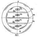
- FIG. 3 shows an arrangement with four detectors lying next to one another in plan view, but without a shielding heat sink.
- the carrier film designated 21 which in the present case is designed as a circular structure.
- four absorber layers, designated 23a, 23b, 23c and 23d, are provided in series, each of which sits on heat-conducting layers 22a, 22b, 22c, 22d.
- the formation of these heat-conducting layers is such that they conform to the circular outline of the carrier film 21 while maintaining the appropriate distances 24a, 24b and 24c.
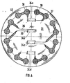
- the bottom view of the carrier film shown in FIG. 4, which is designated here by 31, shows the high-resistance layers 34a, 34b, 34c and 34d. These are located exactly under the absorber layers 23a, 23b, 23c, 23d on the other side of the carrier film, as designated by 21 in FIG. 3, so that there is absorber layer and corresponding high-resistance layer, for example absorber layer 23a and high-resistance layer 34a lie exactly opposite on both sides of the carrier film.
- the high-resistance layers are formed in a meandering shape.
- the individual resistance layers are connected via lines 35, 36, which are provided with reference numerals only for the resistance layer 34b, to inner connection surfaces 37 and 38 which are connected to further outer connection surfaces 39 and 40.
- Such a structure as can be seen from FIGS. 3 and 4 in detail, is not only provided for the measuring device exposed to the radiation, but also for a reference device provided in the measuring system which is not exposed to radiation, but rather is shielded against the radiation to be measured .
- the measuring device exposed to the radiation and the reference device shielded against the radiation are arranged one behind the other in a single housing.
- the resistance layer (s) of the reference device are electrically connected into the Wheatstone bridge 6 according to FIG. 2 and correspond there to the resistor 9.
- FIG. 5 shows the heat sink 41 to be placed on the carrier film with applied heat layers and absorber layers, which has the recesses 42a, 42b, 42c and 42d, which have windows 43a, 43b, 43c and 43d on their top surface.
- the arrangement is clearer from the sectional view according to FIG. 6.
- the heat sink 51 can be seen there with the recesses 53a, 53b, 53c and 53d, in the top surfaces 54a, 54b, 54c and 54d of which windows 55a, 55b, 55c and 55d are provided whose dimensions, like the drawing. 3 clearly shows the dimensions of the absorber layers 23a, 23b, 23c and 23d.
- FIG. 7 shows an exploded perspective view of an embodiment of a measuring system with the measuring device according to the invention and a reference device.
- a cylindrical housing 71 is provided with an inner collar 72 at one end.
- the arrangement designated 73 is supported on this inner collar 72 when it is inserted into the cylindrical housing 71 from the right according to FIG. 7.
- the fixation takes place with the aid of a threaded ring 74, which is screwed into a corresponding internal thread on the other, here right end of the cylindrical housing 71.
- the heat sink just described in connection with FIGS. 5 and 6 is designated by 75 and thus has the corresponding wall thickness and the corresponding recesses and the corresponding windows.
- 76 means the representation of the measuring device exposed to the radiation, consisting of carrier foil and heat conducting layers and absorber layers placed in the direction of the radiation (arrows F).
- a base 77 which consists of an insulating material and is inserted in the contact pins 78, then follows.
- the contact pins 78 protrude through the base 77 and end on the side facing the measuring device 76 in contact areas which can be easily connected to the contact areas on the measuring device 76.
- the underside of the carrier film ie the side carrying the resistance layers, is in contact with a heat sink, namely a cylindrical body made of aluminum, which, however, has recesses such that it does not short-circuit the individual connections and resistance layers.
- a heat sink namely a cylindrical body made of aluminum, which, however, has recesses such that it does not short-circuit the individual connections and resistance layers.
- This heat sink is in the drawing designated with the reference number 79.
- a continuous separating disk 80 then follows, for example an aluminum disk, which completely shields the measuring part of the system (measuring device) against the reference part (reference device).
- a heat sink is designated, which corresponds to the cooling body 75 in all respects.
- a reference device which corresponds to the measuring device 76 in all respects.
- a base 83 which essentially corresponds to the base 77 and carries contact pins 84 corresponding to the contact pins 78.
- These contact pins 84 are offset from the contact pins 78 so that they sit exactly in the middle between the contact pins 78.
- a heat sink is provided which essentially corresponds to the cooler 79.
- Both types of contact pins 78 and 84 are plugged into a common base 86, which is an insulating body similar to the bases 77 and 83.
- connection areas are drilled out on the side of the carrier film carrying the resistance layers, through which the contact pins 78 reach, so that no contact is made between the reference bolometer and the actual measuring bolometer exposed to the radiation, but rather the corresponding row of contacts via the base 83 protrudes and is expediently inserted into an end socket carrying a corresponding number of contacts.
- the measuring and reference device By arranging the measuring and reference device in such a way that the contacts are offset from one another, and by connecting them to a Wheatstone bridge, a compensation of temporally different magnetic fields is achieved. You can achieve this by installing the reference device moreover, a complete compensation of immeasurable radiation parts, which only heat the housing and the parts of the measuring system connected to it, without influencing the measurement.
- the measuring and reference device are arranged side by side and several such device pairs are arranged one behind the other in a row.
- the measuring devices In the right row M the measuring devices should sit in the left row R the reference devices.
- Fig. 9 the structure is indicated in section. 91 means the carrier film, onto which a gold layer 92 is evaporated, which form the heat sink. She has z. B. a thickness of 25 ⁇ m. In this layer 92 recesses 93 and 94 are formed, which have a bottom, the central region 95 and 96 each having an absorber layer of z. B. 4 ⁇ m thickness that directly over an edge region 9 or 98 (vlg. Also Fig. 8), which has a correspondingly smaller thickness of z. B. has only 0.5 microns and forms the heat-conducting layer, merges into the heat sink layer 92. The absorber layer, the heat-conducting layer and the heat sink are therefore in one piece. The production of such a structure in the vapor deposition and etching process presents no difficulties.
- the heat-conducting layer and the heat sink are covered by a cover made of a suitable material and restricting the radiation only to the absorber layer of the measuring device by means of windows.
- the absorber layer is of course also shielded from the incident radiation by this cover.
- the cover is not shown in Fig. 9.
- the windows restricting the radiation onto the desired absorber layers can also be realized by cantilevered edges on the corresponding recesses 93, but this configuration is difficult and also complex.
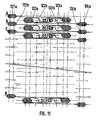
- FIG. 10 shows a pair of high-resistance layers belonging to a pair of measuring and reference devices, which is provided on the side facing away from the measuring and reference device side, measuring and reference devices precisely adapted in their position.
- the arrangements 101 and 102 include not only those belonging to the respective measuring resistor M (cf. resistor 4 according to FIG. 2) or to the respective reference resistor R (cf. resistor 9 according to FIG. 2), here each in the form of a flat meander Resistance winding, but also the winding in the measuring bridge opposite each other, which is also formed as a meander (cf. resistor 8 or 7 according to FIG. 2).
- meanders can, as can be seen in FIG.
- a connecting line leads to a conductor track 104, which is guided around a connection surface 105 and then as the one outer conductor path 106 to the outer connection surface 107.
- a connection line 108 leads from the structure 102 to a conductor track 109, which leads around a connection area 110 and then as the other outer conductor track 111 to the other outer connection area 112.
- the one end on the connecting line 103 The resistance of the structure 101 lies at the other end on the outer conductor 111.
- the resistance of the structure 102 with one end on the connecting line 108 lies at the other end both on an inner conductor 113 leading to the connection surface 110 and on a connecting part 114, which is also connected to the second resistor in the structure 101, which is connected at its other end to the conductor track 115, which leads to the inner connection surface 105.
- one end of the second resistor 102 is connected to the conductor track 115, and its other end lies on the outer conductor track 106.
- FIG. 11 shows the multiple arrangement of such circuits shown in detail in FIG. 10. So that adjacent circuits A, B, C ... N do not mutually interfere with one another, the connection areas 121a and 122a of the circuit A are connected to the AC voltage supply of the bridge circuit, while the connection of the remaining two connection areas 123a and 124a forms the measurement diagonal. In the next circuit B, the connections are reversed, ie the measurement diagonal is between the connection areas 121b and 122b, while the supply diagonal is between the connection areas 123b and 124b. In circuit C, the connection conditions are again like in the circuit A, etc.
- the absorber layer is exposed to the radiation to be measured.
- the radiation absorbed in the absorber layer leads to heating of the absorber layer.
- the heat flows in the direction of the high-resistance layer and towards the sides.
- the resistance layer changes its resistance value measurably, and the clearer the higher the resistance it is.
- the incident radiation leads to a further heating of the absorber layer until the heat flowing off to the sides is equal to the absorbed radiation power.
- the heat is from the massive heat sink with great. heat capacity and negligible heating removed.
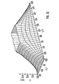
- the change in the resistance of the resistance layer on the side of the carrier film opposite the absorber layer is a measure of the temperature change averaged over the area of the resistance or absorber layer. It can be shown that the temperature change of the detector in response to a step function of the power can be approximately represented by an exponential function of the following form:
- the constants ⁇ eff and c eff are called the bolometer constant.
- the bolometer detector It is therefore important to constructively design the bolometer detector so that the heat flow from the absorber side through the thin carrier film to the resistance layer takes place in a considerably shorter time than the lateral outflow of the heat from the absorber layer to which it is applied limiting heat sink. It is essential that the measuring bolometer facing the radiation source is completely covered with an electrically conductive and heat-conducting layer in order to avoid charging by secondary electrons and to achieve defined heat transport conditions to the heat sink as well as defined characteristic data.
- the outflow of heat can be influenced constructively by increasing or decreasing the thickness of the absorber layer, but also by increasing or decreasing its length or width dimensions.
- the temperature difference ⁇ o of the absorber layer for the detector with a large time constant (B) and that with a small time constant (A) is almost identical, while for long times t the temperature change ⁇ A is less than for the case ( B).
- the higher sensitivity can therefore only be used for longer times, but it is sufficient that the signal-to-noise ratio is approximately 1000.
- a further increase in the time constant leads to a restriction of the dynamics compared to the radiation outputs to be measured and the self-radiation of the absorbers layer is no longer negligible due to the higher detector temperature.
Abstract
Es wird ein Strahlungsmeßgerät (Bolometer) mit einer elektrisch isolierenden Trägerfolie, auf deren einer Seite eine der zu messenden Strahlung auszusetzende, Absorberschicht vorgesehen ist, der gegenüber auf der anderen Seite der Trägerfolie eine hochohmige Widerstandsschicht aufgebracht ist, die Bestandteil einer Widerstandsmeßbrücke ist, beschrieben, bei dem die Absorberschicht in eine seitlich vorstehende mit ihr in thermisch leitendem Kontakt stehende Wärmeleitschicht übergeht und die Wärmeleitschicht gegen die zu messende Strahlung abgeschirmt ist, wobei auch mehrere je eine Absorberschicht tragende Wärmeleitschichten mit Abstand in Reihen nebeneinander angeordnet sein können. Außerdem wird ein Meßsystem mit einem solchen Meßgerät und mit einem zugeordneten, gegen die zu messende Strahlung abgeschirmten Referenzgerät beschrieben, bei dem der Aufbau des Referenzgerätes identisch demjenigen des Meßgerätes entspricht und das Referenzgerät im gleichen Gehäuse wie das Meßgerät angeordnet sind. Bei einer Ausführungsform sind diese beiden Geräte hintereinander angeordnet, während bei einer Ausführungsform Meß- und Referenzgerät nebeneinander sitzen und diese Anordnung in mehrfacher Weise hintereinander wiederholt ist.A radiation measuring device (bolometer) with an electrically insulating carrier film is described, on one side of which an absorber layer to be exposed to the radiation to be measured is provided, and on the other side of the carrier film a high-resistance resistor layer, which is part of a resistance measuring bridge, is applied, in which the absorber layer merges into a laterally protruding heat-conducting layer with which it is in thermally conductive contact and the heat-conducting layer is shielded from the radiation to be measured, it also being possible for a plurality of heat-conducting layers each carrying an absorber layer to be arranged next to one another in rows. In addition, a measuring system with such a measuring device and with an associated reference device shielded against the radiation to be measured is described, in which the structure of the reference device corresponds identically to that of the measuring device and the reference device is arranged in the same housing as the measuring device. In one embodiment, these two devices are arranged one behind the other, while in one embodiment the measuring and reference device sit next to each other and this arrangement is repeated in a number of ways.
Description
Die Erfindung betrifft ein Strahlungsmeßgerät (Bolometer) und richtet sich ferner auf ein unter Verwendung desselben ausgebildetes, aus einem der Strahlung ausgesetzten Meßgerät und einem gegen die Strahlung abgeschirmten Referenzgerät bestehendes Meßsystem.The invention relates to a radiation measuring device (bolometer) and is further directed to a measuring system which is constructed using the same and consists of a measuring device which is exposed to the radiation and a reference device shielded against the radiation.
Bei heutigen großen Plasmamaschinen wird ein wesentlicher Teil der im Plasma deponierten Heizleistung durch elektromagnetische Strahlung und Neutralteilchen zur Wand des Vakuumgefäßes transportiert. Um Aussagen Uber den Energiehaushalt des Plasmas machen zu können, Ist es nötig, über den in Frage kommenden Spektralbereich die Strahlungsleistung, räumlich und zeitlich aufgelöst, absolut zu messen. Der zu messende Spektralbereich erstreckt sich vom Infrarotbereich bis zum Bereich der weichen Röntgenstrahlung im 10 keV-Gebiet.In today's large plasma machines, a substantial part of the heating power deposited in the plasma is transported to the wall of the vacuum vessel by electromagnetic radiation and neutral particles. In order to be able to make statements about the energy balance of the plasma, it is necessary to absolutely measure the radiation power, spatially and temporally resolved, over the spectral range in question. The spectral range to be measured extends from the infrared range to the range of soft X-rays in the 10 keV range.
Für breitbandige Strahlungsmessungen werden als Bolometer bezeichnete Strahlungsmeßgeräte eingesetzt. Dabei handelt es sich um Strahlungsdetektoren, die für einen breiten Spektralbereich (Infrarot bis weiche Röntgenstrahlung) empfindlich sind. Sie messen integral die einfallende Strahlungsleistung. Die Wirkungsweise des Bolometers beruht auf der Absorption der zu messenden Strahlung und einer daraus resultierenden Erwärmung des Bolometerdetektors. Das Bolometersignal ist proportional der Temperaturerhöhung des Detektors und die Empfindlichkeit hängt von dem Temperaturkoeffizienten des zur Messung der Temperaturerhöhung ausgenutzten physikalischen Effektes ab.For broadband radiation measurements, radiation measuring devices called bolometers are used. This is radiation detectors that are sensitive to a wide spectral range (infrared to soft X-rays). They measure the incident radiation power integrally. The action of the bolometer is based on the absorption of the radiation to be measured and the resulting heating of the bolometer detector. The bolometer signal is proportional to the temperature rise of the detector and the sensitivity depends on the temperature coefficient of the physical effect used to measure the temperature rise.
In der Plasmaphysik werden folgende verschiedene Bolometerarten verwendet:
- (1) Halbleiterbolometer (Germaniumschicht)
- (2) Thermistorbolometer (Nickelabsorber mit davon isoliertem Thermistor)
- (3) Gold- oder Platin-Widerstände (freihängend in Mäander- oder Spiralform)
- (4) Pyroelektrische Bolometer
- (5) IR-Bolometer
- (6) Folienbolometer.
- (1) semiconductor bolometer (germanium layer)
- (2) thermistor bolometer (nickel absorber with thermistor isolated from it)
- (3) Gold or platinum resistors (freely hanging in meandering or spiral form)
- (4) Pyroelectric bolometer
- (5) IR bolometer
- (6) Foil bolometer.
Die auf dem Plasma emittierte, auf den Detektor auftreffende Strahlungsleistung liegt in der Größenordnung von wenigen mW. Um diese geringen Strahlungsleistungen messen zu können, empfiehlt sich der Einsatz von Folienbolometern.The radiation power emitted on the plasma and incident on the detector is of the order of a few mW. In order to be able to measure this low radiation power, the use of foil bolometers is recommended.
Folienbolometer bestehen aus drei funktional verschiedenen Elementen,
- a) einer elektrisch isolierenden Trägerfolie mit großer mechanischer Stabilität, auf die eine
- b) hochohmige, aus dünnen und schmalen Bahnen bestehende Widerstandsschicht mit geringer Wärmekapazität in Form eines Mäanders aufgebracht ist. Auf der anderen Seite der Folie liegt genau Uber der Widerstandsschicht eine
- c) Absorberschicht, die allseitig an ihren Rändern von einem Kühlkörper berührt wird.
- a) an electrically insulating carrier film with great mechanical stability, on the one
- b) high-resistance, thin and narrow strips of resistance layer with low heat capacity in the form of a meander is applied. On the other side of the The film lies exactly over the resistance layer
- c) absorber layer, which is touched on all sides at its edges by a heat sink.
Der unmittelbare Zusammenhang zwischen der Zeit für den Wärmeausgleich in Richtung des Kühlkörpers und den Absorberabmessungen führt bei der bisherigen Auslegung von Folienbolometern zu relativ großen Abmessungen des Bolometerdetektors. Detektoren mit großen Abmessungen besitzen allerdings folgende Nachteile: Blendeneffekte der geometrischen Optik, hervorgerufen durch die Abmessungen der Detektoroberfläche in bezug auf den Detektorabstand vom Meßobjekt und dessen Abmessungen.The direct connection between the time for heat compensation in the direction of the heat sink and the absorber dimensions has led to the bolometer detector being relatively large in the design of film bolometers to date. However, detectors with large dimensions have the following disadvantages: Aperture effects of geometric optics, caused by the dimensions of the detector surface in relation to the detector distance from the measurement object and its dimensions.
Relativ große elektrische Kapazität, die den Einsatz von Trägerfrequenz-Signalübertragungen unmöglich macht.Relatively large electrical capacity, which makes the use of carrier frequency signal transmissions impossible.
Empfindlichkeit der Signalübertragung gegen niederfrequente Einstreuungen. Werden Hochfrequenzheizungen für das Plasmaexperiment eingesetzt, sind große Einstreuungen für die Bolometermessungen zu erwarten.Sensitivity of signal transmission to low-frequency interference. If high-frequency heaters are used for the plasma experiment, large interference is to be expected for the bolometer measurements.
Bei Einsatz einer Vielzahl von solchen Meßgeräten ergeben sich bei mäßiger Raumauflösung bereits große zur Unterbringung der Meßgeräte erforderliche Räume.When using a large number of such measuring devices, there are already large rooms required for accommodating the measuring devices with a moderate spatial resolution.
Ausgehend von einem Strahlungsmeßgerät mit einer elektrisch isolierenden Trägerfolie, auf deren einer Seite eine der zu messenden Strahlung auszusetzende Absorberschicht vorgesehen ist, der gegenüber auf der anderen Seite der Trägerfolie eine hochohmige Widerstandsschicht aufgebracht ist, die Bestandteil einer Widerstandsmeßbrücke ist, stellt sich die Erfindung die Aufgabe, das Strahlungsmeßgerät so weiter zu entwickeln, daß es folgenden Forderungen gerecht wird:
- (1) kleine Detektorabmessungen und daraus resultierende
- (a) Möglichkeit höherer Raumauflösung,
- (b) bessere mechanische Festigkeit,
- (c) vernachlässigbare Blendeneffekte der geometrischen Optik,
- (2) kleine elektrische Kapazität,
- (3) vorbestimmte Zeitkonstante,
- (4) Widerstandsfähigkeit gegen Gamma- und Neutronenstrahlung,
- (5) voneinander thermisch unabhängige Detektoren,
- (6) voneinander elektrisch unabhängige Detektoren,
- (7) ausgeschaltete thermische und elektrische Störungen,
- (8) elektrische Durchschlagsfestigkeit,
- (9) Einsatzfähigkeit im Hochvakuum bis 300 °C.
- (1) small detector dimensions and resulting
- (a) possibility of higher spatial resolution,
- (b) better mechanical strength,
- (c) negligible aperture effects of geometric optics,
- (2) small electrical capacity,
- (3) predetermined time constant,
- (4) resistance to gamma and neutron radiation,
- (5) detectors that are thermally independent of one another,
- (6) detectors that are electrically independent of one another,
- (7) switched off thermal and electrical faults,
- (8) dielectric strength,
- (9) Operability in a high vacuum up to 300 ° C.
Gelöst wird diese Aufgabe erfindungsgemäß dadurch, daß die Absorberschicht in eine seitlich vorstehende, mit ihr in thermisch leitendem Kontakt stehende Wärmeleitschicht übergeht und daß die Wärmeleitschicht gegen die zu messende Strahlung abgeschirmt ist. Die Absorberschicht und gegebenenfalls die Wärmeleitschicht können aus einem Edelmetall, vorzugsweise Gold, bestehen. Zweckmäßig ist es, wenn in weiterer Ausbildung der Erfindung die Wärmeleitschicht aus einer die Absorberschicht seitlich überragenden, wesentlich dünneren, gegebenenfalls mit ihr einstückigen und/oder aus dem gleichen Material wie die Absorberschicht gefertigten Schicht besteht.This object is achieved according to the invention in that the absorber layer merges into a laterally protruding heat-conducting layer which is in thermally conductive contact with it and in that the heat-conducting layer is shielded from the radiation to be measured. The absorber layer and optionally the heat conducting layer can consist of a noble metal, preferably gold. It is expedient if, in a further embodiment of the invention, the heat-conducting layer consists of a layer that projects laterally, significantly thinner, possibly in one piece with it and / or is made of the same material as the absorber layer.
Durch die erfindungsgemäße Lösung werden die Energieabsorption und die Wärmeleitung voneinander getrennt, wodurch die Dimensionen des Detektors wesentlich verringert werden können, so daß in weiterer Ausbildung der Erfindung mehrere je eine Absorberschicht tragende Wärmeleitflächen mit Abstand in Reihe nebeneinander angeordnet werden können.The solution according to the invention separates the energy absorption and the heat conduction from one another, as a result of which the dimensions of the detector can be significantly reduced, so that in a further embodiment of the invention a plurality of heat-conducting surfaces, each carrying an absorber layer, can be arranged next to one another in a row.
Man kann die den Absorberschichten zugeordneten hochohmigen Widerstandsschichten jeweils in einer gesonderten Widerstandsmeßbrücke schalten. Ein anderer Weg zu messen besteht darin, daß von den den Absorberschichten zugeordneten hochohmigen Widerstandsschichten wenigstens einige in Reihe geschaltet und die derart gebildeten Widerstandsgruppen in einer gesonderten WiderstandsmeßbrUcke geschaltet sind. Damit kann der Widerstandswert eines Meßsystems entsprechend vergrößert werden, wodurch sich die Brückenspannung bei gleicher auf die Widerstände -aufgebrachter Leistung entsprechend erhöhen und damit die Empfindlichkeit des Meßsystems verbessern läßt. M on can switch the high-resistance layers assigned to the absorber layers in each case in a separate resistance measuring bridge. Another way to measure is that of the high resistance layers associated with the absorber layers at least some connected in series and the resistance groups formed in this way are connected in a separate resistance measuring bridge. The resistance value of a measuring system can thus be increased accordingly, as a result of which the bridge voltage can be increased correspondingly with the same power applied to the resistors and the sensitivity of the measuring system can thus be improved.
In weiterer Ausbildung der Erfindung ist der der hochohmigen Widerstandsschicht in der Meßbrücke gegenüberliegende Festwiderstand ebenfalls als hochohmige Widerstandsschicht ausgebildet und zusammen mit der hochohmigen Widerstandsschicht auf der der Absorberseite abgewendeten Seite der Trägerfolie innerhalb einer der Umgrenzung der Absorberschicht entsprechenden Umgrenzung angeordnet. Mit dieser Maßnahme erreicht man eine doppelte Empfindlichkeit der Meßbrücke. Dies ist darauf zurückzuführen, daß dieser Festwiderstand in seiner nunmehrigen Ausbildung als hochohmige Widerstandsschicht ebenfalls Temperaturänderungen ausgesetzt ist, und zwar denselben wie die ehemals allein der Strahlung ausgesetzte hochohmige Widerstandsschicht.In a further embodiment of the invention, the fixed resistor opposite the high-resistance resistor layer in the measuring bridge is also designed as a high-resistance resistor layer and is arranged together with the high-resistance resistor layer on the side of the carrier film facing away from the absorber within a boundary corresponding to the boundary of the absorber layer. With this measure, a double sensitivity of the measuring bridge is achieved. This is due to the fact that this fixed resistor, as it is now designed as a high-resistance layer, is also exposed to changes in temperature, namely the same as the high-resistance layer that was previously only exposed to radiation.
Wenn in weiterer Ausbildung der Erfindung die Wärmeleitschichten über einen Kühlkörper miteinander verbunden sind, läßt sich die Ausdehnung des gesamten Meßsystems wesentlich verringern, weil dadurch eine wechselseitige Beeinflussung der einzelnen Detektoren wegen der unmittelbaren Abführung der Wärme an die Umgebung über den Kühlkörper unterbunden ist.If, in a further embodiment of the invention, the heat-conducting layers are connected to one another via a heat sink, the extent of the entire measuring system can be significantly reduced because this prevents the individual detectors from interfering with one another because of the direct dissipation of the heat to the environment via the heat sink.
Dabei wird vorzugsweise so vorgegangen, daß der Kühlkörper die Wärmeleitschichten kontaktierende, gegenüber den Dickenabmessungen der Absorber- und Wärmeleitschichten wesentlich größere Dickenabmessungen aufweisende Scheibe aus einem gut wärmeleitenden Material ausgebildet ist, die jeweils im Bereich der Absorberschichten eine Ausnehmung aufweist, deren seitliche Begrenzung einenAbstand von den seitlichen Begrenzungen der Absorberschichten aufweisen und deren jeweilige Deckfläche mit einem Fenster versehen ist, dessen Abmessungen denen der Absorberschicht entspricht.In this case, the procedure is preferably such that the heat sink is in contact with the heat-conducting layers and is much larger than the thickness dimensions of the absorber and heat-conducting layers and is made of a good heat-conducting material, each of which has a recess in the region of the absorber layers, the lateral boundary of which is a distance from the lateral limits of the Have absorber layers and the respective top surface is provided with a window, the dimensions of which correspond to those of the absorber layer.
Alternativ dazu kann der Kühlkörper auch aus dem Material der Wärmeleitschichten bestehen und mit diesen einstückig ausgebildet sein. Zweckmäßig ist dazu auf die Trägerfolie eine Beschichtung aufgetragen, die Ausnehmungen mit jeweils einem Boden aufweist, dessen mittlerer Bereich die Absorberschicht bildet, die über einen dünnen, die Wärmeleitschicht bildenden Randbereich in das Material der Beschichtung übergeht, die als ganzes den Kühlkörper bildet. Mit dieser Maßnahme lassen sich weitaus einfacher besser definierte geometrische Bedingungen für die Begrenzung der Wärmeleitschicht erzielen. Es ist zwar generell möglich, zur Bildung des die Einstrahlung auf die Absorberschicht begrenzenden Fensters die Kühlkörperschicht im Bereich der Wärmeleitschicht hinterschnitten auszubilden. Einfacher ist es aber, wenn in weiterer Ausbildung der Erfindung auf der den Kühlkörper bildenden Beschichtung der Trägerfolie ein Maskenkörper mit die Einstrahlung nur auf die Absorberschichten gewährleistenden Fenstern aufgesetzt ist.As an alternative to this, the heat sink can also consist of the material of the heat-conducting layers and be formed in one piece with them. For this purpose, a coating is expediently applied to the carrier film, which has recesses, each with a bottom, the central region of which forms the absorber layer, which merges into the material of the coating, which forms the heat sink as a whole, via a thin edge region forming the heat-conducting layer. With this measure, it is much easier to achieve better-defined geometric conditions for the limitation of the heat-conducting layer. It is generally possible to undercut the heat sink layer in the region of the heat-conducting layer in order to form the window that limits the radiation onto the absorber layer. However, it is simpler if, in a further embodiment of the invention, a mask body with the radiation that only ensures radiation on the absorber layers is placed on the coating of the carrier film that forms the heat sink.
Vorzugsweise ist der Abstand zwischen der Begrenzung der jeweiligen Ausnehmung und der Begrenzung der jeweiligen Absorberschicht so gewählt, daß der Wärmeübergang zwischen Absorberschicht und hochohmiger Widerstandsschicht wesentlich rascher erfolgt, als der Wärmeübergang von der Begrenzung der Absorberschicht in den Kühlkörper.The distance between the delimitation of the respective recess and the delimitation of the respective absorber layer is preferably selected such that the heat transfer between the absorber layer and the high-resistance resistor layer takes place much faster than the heat transfer from the delimitation of the absorber layer into the heat sink.
ZurEinstellungder Zeitkonstanten des seitlichen Wärmeabflusses von Absorberschicht zum Kühlkörper ist der Abstand der seitlichen Begrenzung der Absorberschichten zum Kühlkörper auf die Dicke der Wärmleitschicht abgestimmt.In order to adjust the time constant of the lateral heat flow from the absorber layer to the heat sink, the distance between the lateral boundary of the absorber layers and the heat sink is matched to the thickness of the heat conducting layer.
Besonders vorteilhaft ist es, wenn zur Erleichterung der Montage auf der die hochohmigen Widerstandsschichten tragenden Seite der Trägerfolie in die Widerstandsschichten umgebender Anordnung lötfähige Anschlußflächen vorgesehen sind.It is particularly advantageous if, in order to facilitate assembly, solderable connection surfaces are provided on the side of the carrier film carrying the high-resistance resistance layers in the arrangement surrounding the resistance layers.
Durch Hinzuschalten eines Referenzgerätes, das möglichst nahe am Meßgerät untergebracht sein soll, können elektrische und thermische Störungen direkt kompensiert werden. Durch Einschalten des Referenzgerätwiderstandes in den zweiten Zweig der Wheatstone'schen Brückenschaltung führen auf beide Detektoren wirkende Effekte zu einer symmetrischen Verstimmung der Brückenzweige und so zu einer Kompensation, die die Abgestimntheit der Brücke erhält. Besitzen beide Detektoren identische Eigenschaften, bleibt die Meßbrücke ideal abgestimmt.By connecting a reference device, which should be located as close as possible to the measuring device, electrical and thermal interference can be compensated for directly. By switching on the reference device resistor in the second branch of the Wheatstone bridge circuit, effects acting on both detectors lead to a symmetrical detuning of the bridge branches and thus to a compensation which maintains the matching of the bridge. If both detectors have identical properties, the measuring bridge remains ideally matched.
Dabei wird die Konstruktion zweckmäßig so gewählt, daß der Aufbau des Referenzgerätes identisch demjenigen des Meßgerätes entspricht und das Referenzgerät im gleichen Gehäuse wie das Meßgerät angeordnet ist.The construction is expediently chosen so that the structure of the reference device is identical to that of the measuring device and the reference device is arranged in the same housing as the measuring device.
Vorzugsweise sind Meßgerät und Referenzbolometer hintereinander im Gehäuse angeordnet.The measuring device and reference bolometer are preferably arranged one behind the other in the housing.
Dadurch ergibt sich ein besonders vorteilhafter Aufbau des Meßsystems, weil die lötfähigen Anschlußflächen auf der die Widerstände tragenden Seite der beiden Trägerfolien doppelt vorhanden sein und hintereinander geschaltet werden können, so daß innere und äußere Anschlußflächen entstehen.This results in a particularly advantageous construction of the measuring system, because the solderable connection surfaces are duplicated on the side of the two carrier foils carrying the resistors and can be connected in series, so that inner and outer connection surfaces are created.
Dabei sind dann beim Meßgerät die äußeren lötfähigen Anschlußflächen mit ersten Kontaktstiften leitend verbunden und beim Referenzgerät die inneren lötfähigen Anschlußflächen mit zweiten Kontaktstiften leitend verbunden, während die äußeren Anschlußflächen ausgebohrt sind.The outer solderable pads are then conductively connected to first contact pins in the measuring device and the inner solderable pads are conductively connected to second contact pins in the reference device, while the outer pads are drilled out.
Durch diese Ausbohrungen greifen die ersten Kontaktstifte frei hindurch und die Enden der ersten und zweiten Kontaktstifte bilden den gemeinsamen Ansehlußkörper des aus dem Meßbolometer und aus dem Referenzbolometer bestehenden Meßsystems.The first contact pins pass freely through these bores and the ends of the first and second contact pins form the common contact body of the measuring system consisting of the measuring bolometer and the reference bolometer.
Das Meßgerät wird zwischen zwei Kühlkörpern mit den ent--sprechenden Ausnehmungen eingespannt und mit mechanisch stabilen Anschlüssen versehen.The measuring device is clamped between two heat sinks with the corresponding recesses and provided with mechanically stable connections.
Bei den Kühlkörpern handelt es sich um Aluminiumscheiben, die die Detektoren auf die Gehäusetemperatur des Meßsystems abkühlen. Der auf der Absorberseite liegende Kühlkörper ist so ausgelegt, daß die Wärmeleitflächen an ihren Rändern von dem darauf aufgesetzten Kühlkörper berührt werden. Dieser Kühlkörper verfügt über Ausfräsungen, die wiederum jeweils ein Fenster aufweisen, das lediglich den Zugang zum Absorber freiläßt.The heat sinks are aluminum disks that cool the detectors to the housing temperature of the measuring system. The heat sink lying on the absorber side is designed so that the heat-conducting surfaces are touched at their edges by the heat sink placed thereon. This heat sink has cutouts, each of which in turn has a window that only allows access to the absorber.
Das Meßgerät kann wegen der scheibenartigen Ausbildung des Kühlkörpers flach montiert werden. Durch Ausnehmungen des auf der Widerstandsseite aufliegenden Kühlkörpers kann das Meßgerät optisch justiert werden.The measuring device can be mounted flat because of the disk-like design of the heat sink. The measuring device can be optically adjusted by recesses in the heat sink resting on the resistance side.
Die Gesamtkonstruktion zeichnet sich durch besonders einfache Montierbarkeit aus. Es ist nur nötig, die Durchführungslöcher durch das Meß- bzw. Referenzgerät für Klemmschrauben und die Kontaktstifte zu stanzen.The overall construction is particularly easy to assemble. It is only necessary to punch the through holes through the measuring or reference device for clamping screws and the contact pins.
Die Meß- und Referenzgeräte können dann montiert und verlötet werden und schließlich kann das Meßsystem einfach zusammengesteckt werden.The measuring and reference devices can then be assembled and soldered and finally the measuring system can simply be plugged together.
Nach der Montage sind alle Bauelemente nur in Meßrichtung auf Druck belastet. Die Druckkräfte halten nicht nur die Konstruktion zusammen, sondern liefern auch den Kontaktdruck zwischen den Anschlußflächen und ihren Kontaktstiften und den Kontaktdruck für die im Sockel körper steckenden Kontaktstifte.After assembly, all components are only subjected to pressure in the measuring direction. The compressive forces not only hold the construction together, but also provide the contact pressure between the connection surfaces and their contact pins and the contact pressure for the contact pins stuck in the base.
Es genügt ein Gewindering, um die zusammengesteckten Einzelelemente zu sichern.A threaded ring is sufficient to secure the assembled individual elements.
Bei einer abgeänderten Ausführungsform des Meßsystems sind Meßgerät und Referenzgerät nebeneinander auf der Trägerfolie angeordnet, wobei selbstverständlich nur das Meßgerät der Strahlung ausgesetzt ist, das Referenzgerät aber gegen die zu messende Strahlung abgeschirmt werden muß.In a modified embodiment of the measuring system, the measuring device and the reference device are arranged side by side on the carrier film, whereby of course only the measuring device is exposed to the radiation, but the reference device must be shielded from the radiation to be measured.
Die Anordnung des Meßsystems in weiterer Ausbildung der Erfindung derart, daß die hochohmigen Widerstandsschichten des Meßgerätes und die hochohmigen Widerstandsschichten des Referenzgerätes jeweils als Mäander ausgebildet und die Mäander der hochohmigen Widerstandsschichten von Meßgerät bzw. Referenzgerät ineinander verzahnt auf der Trägerfolie angeordnet sind und auf voneinander abgewendeten Seiten dieser Nebeneinanderanordnung von Meß- und Referenzgerät je zwei in Anschlußflächen ausmündende Leiterbahnen vorgesehen sind, von denen die äußeren die inneren um die Abschlußflächen dieser inneren Leiterbahnen herum umschlingen, wobei der eine Mäander des einen Bolometers zwischen den beiden äußeren Leiterbahnen und der andere Mäander dieses Bolometers zwischen den inneren Leiterbahnen geschaltet ist, während die beiden Mäander des anderen Bolometers jeweils zwischen einer äußeren und einer inneren Leiterbahn geschaltet sind, ermöglicht eine Ausbildung, die mit einer einzigen Maske ohne jegliche Überschneidung von Leiterbahnen herstellbar ist. Dabei soll der Begriff Mäander selbstverständlich in weitestem Umfang verstanden werden und nicht nur kammartige Gebilde umfassen. Auch spiralförmige Verlegungen lassen sich ineinander verschachteln und ermöglichen Anschlüsse an den-äußeren Spiralenden, wenn sie als hin-und zurücklaufende Doppelspiralen ausgebildet werden. Bei der Wahl des Mäanders wird man immer so vorgehen, daß Anschlüsse in der Ebene des Mäanders möglich sind und nicht solche, die winkelig zu dieser Ebene stehen, erforderlich werden.The arrangement of the measuring system in a further embodiment of the invention is such that the high-resistance layers of the measuring device and the high-resistance layers of the reference device are each formed as meanders and the meanders of the high-resistance layers of the measuring device or reference device are interlocked on the carrier film and on opposite sides This juxtaposition of measuring and reference device each have two conductor tracks opening out into connecting surfaces, of which the outer ones loop around the inner surfaces of the inner conductor tracks, one meander of one bolometer between the two outer conductor tracks and the other meander of this bolometer between is connected to the inner conductor tracks, while the two meanders of the other bolometer are each connected between an outer and an inner conductor track, enables an embodiment which can be carried out with a single mask without j normal overlap of conductor tracks can be produced. The term meander should of course in be understood to the greatest extent and not only include comb-like structures. Spiral routings can also be nested one inside the other and enable connections at the outer spiral ends if they are designed as double spirals running back and forth. When choosing the meander, one will always proceed in such a way that connections are possible in the level of the meander and not those that are angled to this level.
Die angegebene Anordnung kann in weiterer Ausbildung der Erfindung zu mehreren in vorzugsweise symmetrischer Anordnung auf einer Trägerfolie vorgesehen werden.The specified arrangement can be provided in a further embodiment of the invention in a preferably symmetrical arrangement on a carrier film.
Die Zeichnung zeigen in
- Fig. 1 eine schematische Darstellung des Aufbaus eines Folienbolometers nach der Erfindung;
- Fig. 2 eine Brückenschaltung, wie sie für ein Folienbolometer nach Fig. 1 zum Einsatz kommt;
- Fig. 3 eine Draufsicht auf eine Trägerfolie mit vier in Reihe nebeneinander angeordneten Absorberschichten mit ihren zugeordneten Härmeleitschichten bei einer bevorzugten Ausführungsform;
- Fig. 4 eine unteransicht der Trägerfolie nach Fig. 3;
- Fig. 5 eine Ausführungsform eines die Wärmeleitschichten verbindenden Kühlkörpers;
- Fig. 6 einen Schnitt durch den Kühlkörper nach Fig. 5 längs der Linie VI-VI der Fig. 5;
- Fig. 7 eine perspektivische Explosionszeichnung einer bevorzugten Ausführungsform eines Meßsystems nach der Erfindung;
- Fig. 8 eine Teildraufsicht auf eine abgeänderte Ausführungsform eines Meßsystems, bei dem Meß- und Referenzgeräte in mehrfacher Wiederholung nebeneinander angeordnet sind;
- Fig. 9 einen Schnitt längs der Linie IX-IX der Fig. 8, wobei die auf der Unterseite der Trägerfolie vorgesehenen hochohmigen Widerstandsschichten wegen der Schwierigkeit der Wiedergabe von Schnitten so extrem dünner Schichten nicht angedeutet sind;
- Fig. 10 eine Draufsicht auf ein Paar von hochohmigen Widerstandsschichten, wie den jeweiligen Paaren aus Meß- und Referenz-Absorberschicht des Meßsystems nach Fig. 8 und 9 zugeordnet sind, mit ihren Anschlüssen;
- Fig. 11 eine Draufsicht auf eine Vielzahl von Paaren hochohmiger Widerstandsschichten zu der Anordnung aus Meß- und Referenz-Absorberschichten nach Fig. 8;
- Fig. 12 eine schematische Darstellung der Temperaturverteilungsdarstellung von der Absorberschicht über die Wärmeleitschicht zum Kühlkörper;
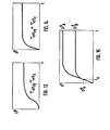
- Fig. 13 eine graphische Darstellung des zeitlichen Temperaturverlaufes in der Widerstandsschicht . bei annähernd gleichen Zeitkonstanten in X-, Y-Richtung bzw. Z-Richtung;
- Fig. 14 eine der Darstellung nach Fig. 13 ähnliche Darstellung, jedoch für eine wesentlich größere Zeitkonstante in X-, Y-Richtung;
- Fig. 15 eine der Darstellung nach Fig. 14 ähnliche Darstellung, jedoch für zwei verschiedene Zeitkonstanten in X-, Y-Richtung.
- Figure 1 is a schematic representation of the structure of a film bolometer according to the invention.
- FIG. 2 shows a bridge circuit as used for a film bolometer according to FIG. 1;
- 3 shows a plan view of a carrier film with four absorber layers arranged in a row next to one another with their associated thermally conductive layers in a preferred embodiment;
- FIG. 4 shows a bottom view of the carrier film according to FIG. 3;
- 5 shows an embodiment of a heat sink connecting the heat-conducting layers;
- 6 shows a section through the heat sink according to FIG. 5 along the line VI-VI of FIG. 5;
- 7 is an exploded perspective view of a preferred embodiment of a measuring system according to the invention;
- 8 is a partial top view of a modified embodiment of a measuring system in which measuring and reference devices are arranged next to one another in multiple repetition;
- 9 shows a section along the line IX-IX of FIG. 8, the high-resistance layers provided on the underside of the carrier film not being indicated because of the difficulty in reproducing sections so extremely thin;
- 10 shows a plan view of a pair of high-resistance layers, as assigned to the respective pairs of measuring and reference absorber layers of the measuring system according to FIGS. 8 and 9, with their connections;
- 11 shows a plan view of a plurality of pairs of high-resistance layers for the arrangement of measuring and reference absorber layers according to FIG. 8;
- 12 shows a schematic representation of the temperature distribution representation from the absorber layer via the heat-conducting layer to the heat sink;
- 13 shows a graphical representation of the temperature profile over time in the resistance layer. with approximately the same time constants in the X, Y and Z directions;
- FIG. 14 shows a representation similar to that shown in FIG. 13, but for a substantially larger time constant in the X, Y direction;
- 15 shows a representation similar to that of FIG. 14, but for two different time constants in the X and Y directions.
In Fig. 1 ist mit 1 eine Trägerfolie aus einem elektrisch isolierenden Material bezeichnet, beispielsweise aus Glimmer oder aus dem unter dem Warenzeichen "Capton" bekannten Kunststoffmaterial. Diese Materialien eignen sich wegen ihrer hohen Strahlenbelastbarkeit und Festigkeit gegenüber hohen Temperaturen besonders gut.In Fig. 1, 1 denotes a carrier film made of an electrically insulating material, for example made of mica or from the plastic material known under the trademark "Capton". These materials are particularly suitable because of their high radiation resistance and strength against high temperatures.
Auf die Trägerfolie 1 ist die Wärmeleitschicht 2 aufgedampft, die vorzugsweise aus Gold oder Platin besteht. Die Dicke dieser Schicht beträgt ca. 0,5 um und weniger.The heat-conducting
In der Mitte dieser Wärmeleitschicht 2 ist eine Absorberschicht 3 aufgedampft, die aus dem gleichen Material wie die Wärmeleitschicht 2 besteht und eine Dicke von ca. 4 µm aufweist. Diese Absorberschicht 3 bildet die Meßfläche. Die Dicke der Absorberschicht 3 ist frei in Abhängigkeit von der zu messenden Strahlung wählbar. Die Schichten 2 und 3 können auch miteinander einstückig sein.In the middle of this heat-conducting
Der Absorberschicht 3 gegenüber befindet sich auf der anderen Seite der Trägerfolie 1 eine hochohmige Widerstandsschicht 4, die beispielsweise mäanderförmig ausgebildet ist und ebenfalls aus ausgedampftem Gold oder Platin bestehen kann.On the other side of the
Der durch die Widerstandsschicht 4 gebildete Widerstand M liegt nach Fig. 2 in einem Zweig 5 einer Wheatstone'schen Brücke 6, die noch drei weitere Widerstände 7, 8 und 9 aufweist, von denen der Widerstand 9 die Widerstandsschicht R eines Referenzgerätes sein kann. Ober die eine Diagonale der Brücke ist ein Meßgerät 10 geschaltet, während an der anderen Diagonale eine Spannung U anliegt. Die Wärmeleitschicht 2 an ihren Rändern berührend ist ein Kühlkörper 11 aufgesetzt, der sich mit VorsprUngen 12 nach innen erstreckt, die eine Abschirmung bilden, welche lediglich den Zugang zur Absorberschicht 3 freiläßt, die von der schematisch angedeuteten Strahlung F getroffen wird. Die Trägerfolie 1 bildet mit der Wärmeleitschicht 2, der Absorberschicht 3 und der Widerstandsschicht 4 den Detektor des auch als Folienbolometer bezeichenbaren Meßgerätes.The resistance M formed by the
In Fig. 3 ist eine Anordnung mit vier nebeneinanderliegenden Detektoren in Draufsicht, allerdings ohne abschirmenden Kühlkörper darstellt. Man erkennt die mit 21 bezeichnete Trägerfolie, die im vorliegenden Fall als kreisförmiges Gebilde ausgeführt ist. Ober den Durchmesser II-II sind in Reihe vier mit 23a, 23b, 23c und 23d bezeichnete Absorberschichten vorgesehen, die jeweils auf Wärmeleitschichten 22a, 22b, 22c, 22d sitzen. Die Ausbildung dieser Wärmeleitschichten ist derart, daß sie sich unter Wahrung entsprechender Abstände 24a, 24b und 24c im Umriß dem kreisförmigen Umriß der Trägerfolie 21 anpassen.3 shows an arrangement with four detectors lying next to one another in plan view, but without a shielding heat sink. One recognizes the carrier film designated 21, which in the present case is designed as a circular structure. Above the diameter II-II, four absorber layers, designated 23a, 23b, 23c and 23d, are provided in series, each of which sits on heat-conducting
Bei der in Fig. 4 wiedergegebenen Unteransicht der Trägerfolie, die hier mit 31 bezeichnet ist, erkennt man die hochohmigen Widerstandsschichten 34a, 34b, 34c und 34d. Diese befinden sich genau am Ort unter den Absorberschichten 23a, 23b,23c, 23d auf der anderen Seite der Trägerfolie, wie sie in Fig. 3 mit 21 bezeichnet ist, so daß sich Absorberschicht und entsprechende hochohmige Widerstandsschicht, beispielsweise Absorberschicht 23a und hochohmige Widerstandsschicht 34a auf den beiden Seiten der Trägerfolie exakt gegenUberliegen. Beim wiedergegebenen Ausführungsbeispiel sind die hochohmigen Widerstandsschichten mäanderförmig ausgebildet. Die einzelnen Widerstandsschichten sind über Leitungen 35, 36, die nur für die Widerstandsschicht 34b im einzelnen mit Bezugszeichen versehen sind, mit inneren Anschlußflächen 37 und 38 verbunden, die mit weiteren äußeren Anschlußflächen 39 und 40 in Verbindung stehen. Ein solches Gebilde, wie es sich aus den Fig. 3 und 4 im einzelnen ergibt, ist nicht nur für das der Strahlung ausgesetzte Meßgerät vorgesehen, sondern auch für ein im Meßsystem vorgesehenes Referenzgerät, das keiner Strahlung ausgesetzt, vielmehr gegen diese zu messende Strahlungabgeschirmt ist.The bottom view of the carrier film shown in FIG. 4, which is designated here by 31, shows the high-
Das der Strahlung ausgesetzte Meßgerät und das gegen die Strahlung abgeschirmte Referenzgerät sind bei der in Fig. 7 dargestellten Ausführungsform in einem einzigen Gehäuse hintereinander angeordnet.In the embodiment shown in FIG. 7, the measuring device exposed to the radiation and the reference device shielded against the radiation are arranged one behind the other in a single housing.
Die Widerstandsschicht(en) des Referenzgerätes sind dabei elektrisch in die Wheatstone'sche Brücke 6 nach Fig. 2 eingeschaltet und entsprechen dort dem Widerstand 9.The resistance layer (s) of the reference device are electrically connected into the
Fig. 5 zeigt den auf die Trägerfolie mit aufgebrachten Wärmeschichten und aufgesetzten Absorberschichten aufzusetzenden Kühlkörper 41, der die Ausnehmungen 42a, 42b, 42c und 42d aufweist, die an ihrer Deckfläche Fenster 43a, 43b, 43c und 43d besitzen.5 shows the
Die Anordnung wird deutlicher aus der Schnittdarstellung nach Fig. 6. Man erkennt dort den Kühlkörper.51 mit den Ausnehmungen 53a, 53b, 53c und 53d, in deren Deckflächen 54a, 54b, 54c und 54d Fenster 55a, 55b, 55c und 55d vorgesehen sind, deren Abmessungen, wie die Zeichnung . im Zusammenhang mit Fig. 3 deutlich erkennen läßt, gleich den Abmessungen der Absorberschichten 23a, 23b, 23c und 23d sind.The arrangement is clearer from the sectional view according to FIG. 6. The
Fig. 7 zeigt eine perspektivische Explosionszeichnung einer Ausführungsform eines Meßsystems mit dem erfindungsgemäßen Meßgerät und einem Referenzgerät. Ein zylindrisches Gehäuse.71 ist an einem Ende mit einem Innenbund 72 versehen. Auf diesem Innenbund 72 stützt sich die mit 73 bezeichnete Anordnug auf, wenn diese von rechts nach Fig. 7 in das zylindrische Gehäuse 71 eingeschoben wird. Die Fixierung erfolgt mit Hilfe eines Gewinderinges 74, der in ein entsprechendes Innengewinde am anderen, hier rechten Ende des zylindrischen Gehäuses 71 eingeschraubt wird.7 shows an exploded perspective view of an embodiment of a measuring system with the measuring device according to the invention and a reference device. A
Mit 75 ist der eben im Zusammenhang mit den Fig. 5 und 6 beschriebene Kühlkörper bezeichnet, der somit die entsprechende Wandstärke und die entsprechenden Ausnehmungen sowie die entsprechenden Fenster aufweist. 76 bedeutet die Darstellung des der Strahlung ausgesetzten Meßgerätes, bestehend aus Trägerfolie und in Richtung der Einstrahlung (Pfeile F) aufgesetzten Wärmeleitschichten und Absorberschichten. Es folgt dann ein Sockel 77, der aus einem Isoliermaterial besteht und in den Kontaktstifte 78 eingesetzt sind. Die Kontaktstifte 78 ragen durch den Sockel 77 hindurch und enden auf dem Meßgerät 76 zugewendeten Seite in Kontaktflächen, die sich leicht mit den Kontaktflächen auf dem Meßgerät 76 verbinden lassen. Auch die Unterseite der Trägerfolie, d. h. die die Widerstandsschichten tragende Seite steht mit einem Kühlkörper in Kontakt, nämlich einem zylindrischen Körper aus Aluminium, der jedoch solche Ausnehmungen aufweist, daß er die einzelnen Anschlüsse und Widerstandsschichten nicht kurzschließt. Dieser Kühlkörper ist in der Zeichnung mit dem Bezugszeichen 79 bezeichnet.The heat sink just described in connection with FIGS. 5 and 6 is designated by 75 and thus has the corresponding wall thickness and the corresponding recesses and the corresponding windows. 76 means the representation of the measuring device exposed to the radiation, consisting of carrier foil and heat conducting layers and absorber layers placed in the direction of the radiation (arrows F). A
Es folgt dann eine durchgehende Trennscheibe 80, beispielsweise eine Aluminiumscheibe, die den messenden Teil des Systems (Meßgerät) gegen den Referenzteil (Referenzgerät) vollständig abschirmt. Mit 81 ist ein Kühlkörper bezeichnet, der dem KUhlkörper 75 in jeder Hinsicht entspricht. Mit 82 Ist ein Referenzgerät bezeichnet, das dem Meßgerät 76 in jeder Hinsicht entspricht.Daran schließt sich ein Sockel 83 an, der im wesentlichen dem Sockel 77 entspricht und Kontaktstifte 84 entsprechend den Kontaktstiften 78 trägt. Diese Kontaktstifte 84 sind gegenüber den Kontaktstiften 78 so versetzt, daß sie genau mittig zwischen den Kontaktstiften 78 sitzen. Auch hier Ist wieder ein Kühlkörper vorgesehen, der im wesentlichen dem KUhlkörper 79 entspricht. Beide Arten von Kontaktstiften 78 bzw. 84 sind in einen gemeinsamen Sockel 86 gesteckt, bei dem es sich um einen Isolierkörper ähnlich wie bei den Sockeln 77 und 83 handelt.A
Auf dem Referenzgerät 82 sind diejenigen Anschlußflächen auf der die Widerstandsschichten tragenden Seite der Trägerfolie ausgebohrt, durch die die Kontaktstifte 78 hindurchgreifen, so daß kein Kontakt zwischen dem Referenzbolometer und dem eigentlichen, der Strahlung ausgesetzten Meßbolometer entsteht, vielmehr die entsprechende Reihe von Kontakten über den Sockel 83 vorsteht und zweckmäßig in einem eine entsprechende Anzahl von Kontakten tragenden Abschlußsockel eingesteckt ist.On the
Durch die Anordnung von Meß- und Referenzgerät derart, daß die Kontakte gegeneinander versetzt sind, und durch die Einschaltung in eine Wheatstone'sche Brücke erreicht man eine Kompensation zeitlich verschiedeler Magnetfelder. Durch den gewählten Einbau des Referenzgerätes erreicht man darüber hinaus eine vollständige Kompensation nicht meßbarer Strahlungsteile, die lediglich das Gehäuse und die mit Ihm in Verbindung stehenden Teile des Meßsystems erwärmen, ohne daß die Messung beeinflußt wird.By arranging the measuring and reference device in such a way that the contacts are offset from one another, and by connecting them to a Wheatstone bridge, a compensation of temporally different magnetic fields is achieved. You can achieve this by installing the reference device moreover, a complete compensation of immeasurable radiation parts, which only heat the housing and the parts of the measuring system connected to it, without influencing the measurement.
Bei der Ausführungsform nach Fig. 8 sind Meß- und Referenzgerät nebeneinander und mehrere solcher Gerätepaare hintereinander in je einer Reihe angeordnet. In der rechten Reihe M sollen die Meßgeräte in der linken Reihe R die Referenzgeräte sitzen.In the embodiment according to FIG. 8, the measuring and reference device are arranged side by side and several such device pairs are arranged one behind the other in a row. In the right row M the measuring devices should sit in the left row R the reference devices.
In Fig. 9 ist im Schnitt der Aufbau angedeutet. 91 bedeutet die Trägerfolie, auf die eine Goldschicht 92 aufgedampft ist, welche den Kühlkörper bilden. Sie hat z. B. eine Dicke von 25 um. In dieser Schicht 92 sind Ausnehmungen 93 und 94 ausgeformt, die einen Boden aufweisen, dessen mittlerer Bereich 95 bzw. 96 jeweils eine Absorberschicht von z. B. 4µm Dicke bildet, die unmittelbar über einen Randbereich 9 bzw. 98 (vlg. auch Fig. 8), der eine entsprechend geringere Dicke von z. B. nur 0,5 um aufweist und die Wärmeleitschicht bildet, in die Kühlkörperschicht 92 übergeht. Absorberschicht, Wärmeleitschicht und Kühlkörper sind also einstückig. Die Herstellung eines solchen Gebildes im Aufdampf- und Ätzverfahren bereitet keine Schwierigkeiten.In Fig. 9 the structure is indicated in section. 91 means the carrier film, onto which a
Bei der in Fig. 8 und 9 wiedergegebenen Ausführungsform erfolgt die Abdeckung der Wärmeleitschicht und des Kühlkörpers durch eine mittels Fenster die Einstrahlung nur auf die Absorberschicht des Meßgerätes beschränkende Abdeckung aus geeignetem Material. Für die Referenzgeräte ist die Absorberschicht selbstverständlich ebenfalls durch diese Abdeckung gegen die einfallende Strahlung abgeschirmt. Die Abdeckung ist in Fig. 9 nicht dargestellt. Man kann die die Einstrahlung auf die gewünschten Absorberschichten beschränkenden Fenster auch durch überkragende Ränder an den entsprechenden Ausnehmungen 93 verwirklichen, jedoch ist diese Ausgestaltung schwierig und auch aufwendig.In the embodiment shown in FIGS. 8 and 9, the heat-conducting layer and the heat sink are covered by a cover made of a suitable material and restricting the radiation only to the absorber layer of the measuring device by means of windows. For the reference devices, the absorber layer is of course also shielded from the incident radiation by this cover. The cover is not shown in Fig. 9. The windows restricting the radiation onto the desired absorber layers can also be realized by cantilevered edges on the corresponding recesses 93, but this configuration is difficult and also complex.
In Fig. 10 ist ein zu einem Meß- und Referenzgerätepaar gehörendes Paar von hochohmigen Widerstandsschichten wiedergegeben, die auf der von der Meß- und Referenzgeräteseite abgewendeten Seite, Meß- und Referenzgeräte in ihrer Lage genau angepaßt, vorgesehen ist. Dabei umfassen die Anordnungen 101 und 102 nicht nur die zum jeweiligen Meßwiderstand M (vgl. Widerstand 4 nach Fig. 2) bzw. zum jeweiligen Referenzwiderstand R (vgl. Widerstand 9 nach Fig. 2) gehörende, hier in Form jeweils eines flachen Mäanders ausgebildete Widerstandswicklung, sondern auch die in der Meßbrücke jeweils gegenüberliegende ebenfalls als Mäander ausgebildete Wicklung (vgl. Widerstand 8 bzw. 7 nach Fig. 2). Solche Mäander lassen sich, wie Fig. 10 erkennen läßt, ineinander verzahnen oder verschachteln, so daß jeweils ein beide Widerstände umfassendes flächiges Gebilde entsteht. Aus diesen flächigen Gebilden 101 und 102 lassen sich die Brückeneckknoten so herausführen, daß nirgends eine Oberschneidung entsteht, wodurch die Herstellung der Anordnung wesentlich erleichtert ist.FIG. 10 shows a pair of high-resistance layers belonging to a pair of measuring and reference devices, which is provided on the side facing away from the measuring and reference device side, measuring and reference devices precisely adapted in their position. The
Vom Ende 103 einer der mäanderartigen Widerstände des Gebildes 101 führt eine Anschlußleitung zu einer Leiterbahn 104, die um eine Anschlußfläche 105 herum und dann als die eine äußere Leiterbahn 106 zur äußeren Anschlußfläche 107 geführt ist. Vom Gebilde 102 führt eine Anschlußleitung 108 zu einer Leiterbahn 109, die um eine Anschlußfläche 110 herum und dann als die andere äußere Leiterbahn 111 zur anderen äußeren Anschlußfläche 112 führt. Der mit dem einen Ende an der Anschlußleitung 103 liegende Widerstand des Gebildes 101 liegt am anderen Ende an der äußeren Leiterbahn 111. Der mit dem einen Ende an der Anschlußleitung 108 liegende Widerstand des Gebildes 102 liegt mit dem anderen Ende sowohl an einer inneren, zur Anschlußfläche 110 führenden Leiterbahn 113 als auch an einem Verbindungsteil 114, der auch mit dem zweiten Widerstand im Gebilde 101 verbunden ist, welcher mit seinem anderen Ende an die Leiterbahn 115 angeschaltet ist, die zur inneren Anschlußfläche 105 führt. Außerdem ist an die Leiterbahn 115 das eine Ende des zweiten Widerstandes 102 angeschaltet, der mit seinem anderen Ende an der äußeren Leiterbahn 106 liegt. Verfolgt man die einzelnen Verbindungen, so ergibt die Gesamtanordnung die Brückenschaltung nach Fig. 2, wobei jedoch Meßwiderstand und gegenüberliegender Widerstand 8 bzw. Referenzwiderstand 9 und sein gegenüberliegender Widerstand 7 jeweils in der Umgrenzung eines vorgegebenen Feldes liegen, dem auf der anderen Seite der Trägerfolie die jeweiligen Absorberschichten von Meß- bzw. Referenzgerät gegenüberliegen.From the
Fig. 11 zeigt die Mehrfachanordnung solcher in Fig. 10 im einzelnen wiedergegebener Schaltungen. Damit sich benachbarte Schaltungen A, B, C ....N nicht wechselseitig elektrisch stören, sind die Anschlußflächen 121a und 122a der Schaltung A an die Wechselspannungsversorgung der Brückenschaltung gelegt, während die Verbindung der restlichen beiden Anschlußflächen 123a und 124a die Meßdiagonale bildet. Bei der nächsten Schaltung B liegen die Anschlüsse umgekehrt, d. h. zwischen den Anschlußflächen 121b und 122b befindet sich die Meßdiagonale, während die Versorgungsdiagonale zwischen den Anschlußflächen 123b und 124b liegt. Bei der Schaltung C liegen die Anschlußverhältnisse wieder wie bei der Schaltung A usw. Es liegen also immer Meßleitungen bzw. Versorgungsleitungen nebeneinander, so daß sich allenfalls immer geringe Spannungen der Meßleitungen bzw. hohe Spannungen der Versorgungsleitungen beeinflussen und nicht die hohe Spannung an einer Versorgungsleitung auf die geringe Spannung an einer Meßleitung einstreut. Es ist also dafür gesorgt, daß die äußeren Leiterbahnen 106 und 111 (Fig. 10) benachbarter Schaltungen immer gleiche Potentiale führen.FIG. 11 shows the multiple arrangement of such circuits shown in detail in FIG. 10. So that adjacent circuits A, B, C ... N do not mutually interfere with one another, the
Im folgenden soll anhand der Fig. 12 bis 15 die Wirkungsweise eines Gerätes nach der Erfindung näher erläutert werden:
- Fig. 12 zeigt räumlich den Temperaturverlauf von der an der Absorberschicht (oben) herrschenden höchsten Temperatur bis zum Kühlkörper (Umgebungstemperatur) für den Zeitpunkt t.
- FIG. 12 spatially shows the temperature profile from the highest temperature prevailing at the absorber layer (top) to the heat sink (ambient temperature) for the time t.
Die Absorberschicht ist der zu messenden Strahlung ausgesetzt. Die in der Absorberschicht absorbierte Strahlung führt zu einer Erwärmung der Absorberschicht. Die Wärme fließt in Richtung der hochohmigen Widerstandsschicht und zu den Seiten hin ab. Die Widerstandsschicht ändert ihren Widerstandswert meßbar, und zwar umso deutlicher, je hochohmiger sie ist. Die auftreffende Strahlung führt solange zu einer weiteren Erhitzung der Absorberschicht, bis die zu den Seiten hin abfließende Wärme gleich der absorbierten Strahlungsleistung ist. Die Wärme wird dabei von dem massereichen Kühlkörper mit großer . wärmekapazität und zu vernachlässigender Aufheizung abtransportiert. Die Änderung des Widerstandes der Widerstandsschicht auf der der Absorberschicht gegenüberliegenden Seite der Trägerfolie ist ein Maß für die über die Fläche der Widerstands- bzw. Absorberschicht gemittelte Temperaturänderung. Man kann zeigen, daß die Temperaturänderung des Detektors als Antwort einer Sprungfunktion der Leistung näherungsweise durch eine Exponentialfunktion folgender Form dargestellt werden kann:
Die Konstanten τeff und ceff werden Bolometerkonstante genannt.The constants τ eff and c eff are called the bolometer constant.
Die Näherung gilt allerdings nur, wenn die Zeit für den Temperaturausgleich in Richtung der Widerstandsschicht wesentlich schneller als der Temperaturausgleich zu den Seiten hin erfolgt. Die Zeitkonstante τ effxy der Wärmeleitung in X- und Y-Richtung muß also wesentlich größer sein, als die in Z-Richtung geltende Zeitkonstante τeffz. Der Grund dafür läßt sich in zwei Diagrammen verdeutlichen, die in Fig. 13 und 14 wiedergegeben sind.The approximation only applies, however, if the time for the temperature compensation in the direction of the resistance layer takes place much faster than the temperature compensation towards the sides. The time constant τ eff xy of the heat conduction in the X and Y directions must therefore be substantially greater than the time constant τeff z in the Z direction. The reason for this can be illustrated in two diagrams, which are shown in FIGS. 13 and 14.
In ersten Fall (Fig. 13) ergibt sich eine schwierige Beschreibung der thermischen Vorgänge, um von der Temperaturänderung und der daraus folgenden meßbaren Widerstandsänderung des Bolometerwiderstandes auf die einfallende Leistung zu schließen, während für den zweiten Fall (Fig. 14) für zeitlich sich verändernde Strahlungsleistungen mit Gleichung 1.) aus der Theorie der Differentialgleichung folgt
Es kommt also darauf an, den Bolometerdetektor konstruktiv so auszulegen, daß der Wärmefluß von der Absorberseite durch die dünne Trägerfolie auf die Widerstandsschicht in wesentlich kürzerer Zeit erfolgt, als der seitliche Abfluß der Wärme von der Absorberschicht zu dem sie begrenzenden KUhlkörper. Es Ist dabei wesentlich, daß das der Strahlungsquelle zugewendete Meßbolometer völlig mit einer elektrisch leitenden und wärmeleitenden Schicht bedeckt ist, um Aufladung durch Sekundärelektronen zu vermeiden und definierte Wärmetransportbedingungen zum Kühlkörper sowie definierte Kenndaten zu erreichen.It is therefore important to constructively design the bolometer detector so that the heat flow from the absorber side through the thin carrier film to the resistance layer takes place in a considerably shorter time than the lateral outflow of the heat from the absorber layer to which it is applied limiting heat sink. It is essential that the measuring bolometer facing the radiation source is completely covered with an electrically conductive and heat-conducting layer in order to avoid charging by secondary electrons and to achieve defined heat transport conditions to the heat sink as well as defined characteristic data.
Der Abfluß der Wärme kann konstruktiv durch Vergrößerung bzw. Verkleinerung der Dicke der Absorberschicht, aber auch durch Vergrößerung bzw. Verkleinerung ihrer Längen- bzw. Breitenabmessungen beeinflußt werden.The outflow of heat can be influenced constructively by increasing or decreasing the thickness of the absorber layer, but also by increasing or decreasing its length or width dimensions.
Bei gegebener Dicke ergibt sich für eine Vergrößerung der Zeitkonstante eine entsprechende Vergrößerung der Längen- bzw. Breitenabmessungen. Eine Verringerung der Dicke wurde eine Verkleinerung der seitlichen Abmessungen bei gleicher Zeitkonstante verlangen. Die Zeitkonstante darf allerdings nicht beliebig groß gewählt werden, da dies einerseits zu einer größeren Erhitzung des Detektors, aber andererseits zu keiner ausnutzbaren Erhöhung der Empfindlichkeit des Bolometers führt. Das Diagramm in Fig. 15 verdeutlicht diesen Sachverhalt.For a given thickness, a corresponding increase in the length or width dimensions results for an increase in the time constant. A reduction in the thickness would require a reduction in the lateral dimensions with the same time constant. However, the time constant must not be chosen to be arbitrarily large, since on the one hand this leads to greater heating of the detector, but on the other hand it does not lead to an exploitable increase in the sensitivity of the bolometer. The diagram in FIG. 15 illustrates this fact.
Für die kurze Zeit to ist die Temperaturdifferenz νo der Absorberschicht für den Detektor mit großer Zeitkonstante (B) und dem mit kleiner Zeitkonstante (A) nahezu identisch, während für lange Zeiten t die Temperaturänderung νA geringer ist, als für den Fall (B). Man kann also nur für größere Zeiten die höhere Empfindlichkeit ausnutzen, wobei es aber genügt, daß das Signal-Rausch-Verhältnis ungefähr den Wert 1000 hat. Außerdem führt eine weitere Erhöhung der Zeitkonstante zu einer Einschränkung der Dynamik gegenüber den zu messenden Strahlungsleistungen und die Eigenabstrahlung der Absorberschicht wird durch die höhere Detektortemperatur nicht mehr vernachlässigbar.For the short time t o , the temperature difference ν o of the absorber layer for the detector with a large time constant (B) and that with a small time constant (A) is almost identical, while for long times t the temperature change ν A is less than for the case ( B). The higher sensitivity can therefore only be used for longer times, but it is sufficient that the signal-to-noise ratio is approximately 1000. In addition, a further increase in the time constant leads to a restriction of the dynamics compared to the radiation outputs to be measured and the self-radiation of the absorbers layer is no longer negligible due to the higher detector temperature.
Im Zusammenhang mit Fig. 2 ist noch auf eine besonders vorteilhafte Möglichkeit des Einsatzes des erfindungsgemäßen Meßsystems hinzuweisen.In connection with FIG. 2, a particularly advantageous possibility of using the measuring system according to the invention should also be pointed out.
Wählt man als Spannung U eine Gegentaktwechselspannung, dann liegt am oberen Spannungsanschluß eine zum unteren Spannungsanschluß um 180° versetzte Wechselspannung an.If a push-pull alternating voltage is selected as the voltage U, then an alternating voltage offset from the lower voltage connection by 180 ° is present at the upper voltage connection.
Dies hat zur Folge, daß bei abgeglichener Brücke die Meßdiagonale immer den Spannungswert Null hat. Dadurch ergibt sich die Möglichkeit der Messung gegen den Nullwert und man erhält somit Meßsignale, die erheblich verstärkbar sind, weil keinerlei Versetzung (Offset) vorliegt. Ein weiterer Vorteil ergibt sich daraus, daß wegen dieser Art der Wechselspannungsversorgung der Wheatstone'schen Brücke eine Auswertung nach der Log-In-Technologie erfolgen kann.The consequence of this is that when the bridge is balanced, the measurement diagonal always has the voltage value zero. This results in the possibility of measuring against the zero value, and measurement signals are obtained which can be amplified considerably because there is no offset. Another advantage arises from the fact that, because of this type of AC voltage supply to the Wheatstone bridge, an evaluation can be carried out using the log-in technology.
Claims (26)
Applications Claiming Priority (4)
| Application Number | Priority Date | Filing Date | Title |
|---|---|---|---|
| DE3401946 | 1984-01-20 | ||
| DE3401946 | 1984-01-20 | ||
| DE3408724 | 1984-03-09 | ||
| DE3408724A DE3408724A1 (en) | 1984-01-20 | 1984-03-09 | RADIATION MEASURING DEVICE AND USING THE SAME TRAINED, FROM A MEASURING DEVICE EXPOSED TO RADIATION AND A REFERENCE DEVICE PROTECTED FROM RADIATION |
Publications (3)
| Publication Number | Publication Date |
|---|---|
| EP0149819A2 true EP0149819A2 (en) | 1985-07-31 |
| EP0149819A3 EP0149819A3 (en) | 1986-07-16 |
| EP0149819B1 EP0149819B1 (en) | 1989-07-19 |
Family
ID=25817750
Family Applications (1)
| Application Number | Title | Priority Date | Filing Date |
|---|---|---|---|
| EP84115783A Expired EP0149819B1 (en) | 1984-01-20 | 1984-12-19 | Radiation gauge, and arrangement using such a gauge exposed to radiation, as well as a sheltered reference gauge |
Country Status (4)
| Country | Link |
|---|---|
| US (1) | US4687342A (en) |
| EP (1) | EP0149819B1 (en) |
| JP (1) | JP2622539B2 (en) |
| DE (2) | DE3408724A1 (en) |
Families Citing this family (14)
| Publication number | Priority date | Publication date | Assignee | Title |
|---|---|---|---|---|
| JPS6275369A (en) * | 1985-09-30 | 1987-04-07 | Toshiba Corp | Radiation detector |
| US4904869A (en) * | 1988-12-14 | 1990-02-27 | Progress Technologies Corporation | X-ray sensor having a high mass number convertor and a superconducting detector |
| DE3927735A1 (en) * | 1989-08-23 | 1991-02-28 | Asea Brown Boveri | Radiation thermometer with meandering thin film resistor - mounted on coated plastics foil tensioned across cavity of substrate material and fixed by adhesive |
| US5634718A (en) * | 1994-07-27 | 1997-06-03 | The United States Of America As Represented By The Secretary Of Commerce | Particle calorimeter with normal metal base layer |
| DE19527226A1 (en) * | 1995-07-26 | 1997-01-30 | Applied Precision S R O | Thermo-electric measurement converter - has electronically controlled resistance and temperature sensor and sums input signal and sensor signal to form output signal |
| EP0794415A1 (en) * | 1996-03-06 | 1997-09-10 | Koninklijke Philips Electronics N.V. | Contactless temperature measuring device |
| DE19808132B4 (en) * | 1997-02-27 | 2009-10-29 | Ust Umweltsensortechnik Gmbh | Component for transmitting and receiving infrared radiation |
| ITMI20012475A1 (en) * | 2001-11-23 | 2003-05-23 | Luigi Argenti | INSTRUMENT FOR MEASURING THE POWER OF RADIATION EMITTED BY A LASER SOURCE AND PROCEDURE IMPLEMENTED FOR MEASURING POWER |
| US7125163B2 (en) * | 2003-11-24 | 2006-10-24 | The Boeing Company | Simple high accuracy high energy calorimeter |
| ITMI20051090A1 (en) * | 2005-06-13 | 2006-12-14 | Laser Point S R L | "ACTING TO DETECT LASER BEAM OPTICAL" |
| US7777887B2 (en) * | 2007-04-13 | 2010-08-17 | Ion Optics, Inc. | Absorption spectroscopy apparatus and method |
| US9933312B2 (en) * | 2016-09-08 | 2018-04-03 | Robert Bosch Gmbh | Bolometer fluid flow and temperature sensor |
| JP7030640B2 (en) * | 2018-07-26 | 2022-03-07 | 株式会社東芝 | Radiation detector and radiation detector |
| JP2023512586A (en) * | 2020-02-06 | 2023-03-27 | トリナミクス ゲゼルシャフト ミット ベシュレンクテル ハフツング | Temperature detection with differential dual detector |
Family Cites Families (12)
| Publication number | Priority date | Publication date | Assignee | Title |
|---|---|---|---|---|
| DE106082C (en) * | ||||
| DE61359C (en) * | TH. PH. CH. CRAMPTON in London, 10 Cursitor Street, Chancery Lane, und A. ESSINGER in Frankfurt a. M., Eckenheimer Landstr. 20; Ver_ treter: F. C. GLASER, Königl. Geh. Kommission^, rath, in Berlin S.W., Lindenstrafse 80. Vom 5. Ju!j 1890 ab | Charcoal holder for arc lamps | ||
| US2986034A (en) * | 1957-10-18 | 1961-05-30 | Robert C Jones | Air-backed thermistor bolometer |
| US3229235A (en) * | 1960-05-02 | 1966-01-11 | Hughes Aircraft Co | Thermal radiant energy detecting device |
| US3535523A (en) * | 1967-02-01 | 1970-10-20 | Hewlett Packard Co | Radiant flux measuring apparatus of the thermopile type |
| US3693011A (en) * | 1971-02-02 | 1972-09-19 | Hughes Aircraft Co | Ion implanted bolometer |
| DD106082A1 (en) * | 1973-06-27 | 1974-05-20 | ||
| US3939706A (en) * | 1974-04-10 | 1976-02-24 | The Boeing Company | High energy sensor |
| US4001586A (en) * | 1975-05-09 | 1977-01-04 | Plessey Incorporated | Thick film sensor and infrared detector |
| US4061917A (en) * | 1976-05-24 | 1977-12-06 | Goranson Rex W | Bolometer |
| US4063095A (en) * | 1976-12-10 | 1977-12-13 | Solomon Wieder | Balancing radiometer |
| JPS57172784A (en) * | 1981-04-17 | 1982-10-23 | Univ Kyoto | Thermoelectric conversion element |
-
1984
- 1984-03-09 DE DE3408724A patent/DE3408724A1/en active Granted
- 1984-12-19 DE DE8484115783T patent/DE3479051D1/en not_active Expired
- 1984-12-19 EP EP84115783A patent/EP0149819B1/en not_active Expired
-
1985
- 1985-01-18 JP JP60007331A patent/JP2622539B2/en not_active Expired - Lifetime
- 1985-01-18 US US06/692,843 patent/US4687342A/en not_active Expired - Lifetime
Non-Patent Citations (4)
| Title |
|---|
| ANALYTICAL CHEMISTRY, Band 51, Nr. 6, Mai 1979, Seiten 712-717; D.G. TAYLOR et al.: "Light entensity measurements I: large area bolometers with microwatt sensitivities and absolute calibration of the Rhodamine B quantum counter" * |
| MESSEN UND PR]FEN, Nr. 3, März 1982, Seiten 164-167, Bad Wörlshofen, DE; "Dünne Schichten für Messgrössenwandler" * |
| REVIEW OF SCIENTIFIC INSTRUMENTS, Band 53, Nr. 10, Oktober 1982, Seiten 1527-1534, New York, US; J. SCHIVELL et al.: "Bolometer for measurements on high-temperature" * |
| TECHNISCHES MESSEN, Band 49, Nr. 10, Oktober 1982, Seiten 355-357, M}nchen, DE; R. HARTMANN et al.: "Hochempfindliche Bolometer in D}nnschichttechnik" * |
Also Published As
| Publication number | Publication date |
|---|---|
| DE3479051D1 (en) | 1989-08-24 |
| JP2622539B2 (en) | 1997-06-18 |
| EP0149819B1 (en) | 1989-07-19 |
| EP0149819A3 (en) | 1986-07-16 |
| DE3408724C2 (en) | 1988-10-27 |
| DE3408724A1 (en) | 1985-07-25 |
| JPS60161580A (en) | 1985-08-23 |
| US4687342A (en) | 1987-08-18 |
Similar Documents
| Publication | Publication Date | Title |
|---|---|---|
| EP0149819B1 (en) | Radiation gauge, and arrangement using such a gauge exposed to radiation, as well as a sheltered reference gauge | |
| DE2806858C2 (en) | ||
| DE69830345T2 (en) | THERMAL FLOW FLOW MEASUREMENT OR MEASUREMENT OF OTHER PROPERTIES OF A FLUID BY DETERMINING A FREQUENCY | |
| EP0607595A2 (en) | Sensor chip | |
| DE4436876A1 (en) | Sensor chip | |
| WO2003062854A2 (en) | Detector for detecting particle beams and method for the production thereof | |
| DE2017067B2 (en) | Pyroelectric detector | |
| EP3546931B1 (en) | Thermoresistive gas sensor, flow sensor and thermal conductivity sensor | |
| DE2948742C2 (en) | ||
| DE2949862A1 (en) | SOLID RADIATION RADIATION DETECTOR AND ARRANGEMENTS THEREOF | |
| DE3438764A1 (en) | THERMOELECTRIC DETECTOR | |
| EP0030056B1 (en) | Influence probing arrangement and method for its realization | |
| EP0584866B1 (en) | Squid-magnetometer with a shielding envelope against electromagnetic interference fields | |
| DE4320326A1 (en) | Device for measuring a radial gas or liquid flow with a Wheatstone bridge of four temperature-sensitive resistors | |
| DE3906981A1 (en) | SUPRAL-CONDUCTING GRADIOMETER FOR MEASURING LOW MAGNETIC FIELDS AND A METHOD FOR THE PRODUCTION THEREOF | |
| DE19711874C2 (en) | Foil pressure gauge | |
| EP0123062A1 (en) | Current divider for a measuring transformer for the measurement of a current | |
| DE3142949C2 (en) | ||
| WO1998043058A9 (en) | Foil manometer | |
| DE2923799C2 (en) | Diffused semiconductor resistance | |
| DE2653865C2 (en) | ||
| DE4208135A1 (en) | Arrangement for measuring gas or liquid flow - contains four temp. dependent resistances forming two sensors in Wheatstone bridge | |
| DE69531266T2 (en) | magnetic sensor | |
| DE19746199A1 (en) | Magnetoresistive angle sensor for angle and position measurement | |
| DE3822164A1 (en) | Heat flow sensor |
Legal Events
| Date | Code | Title | Description |
|---|---|---|---|
| PUAI | Public reference made under article 153(3) epc to a published international application that has entered the european phase |
Free format text: ORIGINAL CODE: 0009012 |
|
| AK | Designated contracting states |
Designated state(s): CH DE FR GB IT LI SE |
|
| RIN1 | Information on inventor provided before grant (corrected) |
Inventor name: MUELLER, REINHOLD, DR. Inventor name: MAST, KARL-FRIEDRICH, DR.-PHYS. Inventor name: BETZLER, PETER, DIPL.-ING. |
|
| PUAL | Search report despatched |
Free format text: ORIGINAL CODE: 0009013 |
|
| AK | Designated contracting states |
Kind code of ref document: A3 Designated state(s): CH DE FR GB IT LI SE |
|
| 17P | Request for examination filed |
Effective date: 19860812 |
|
| 17Q | First examination report despatched |
Effective date: 19880321 |
|
| GRAA | (expected) grant |
Free format text: ORIGINAL CODE: 0009210 |
|
| AK | Designated contracting states |
Kind code of ref document: B1 Designated state(s): CH DE FR GB IT LI SE |
|
| REF | Corresponds to: |
Ref document number: 3479051 Country of ref document: DE Date of ref document: 19890824 |
|
| ITF | It: translation for a ep patent filed |
Owner name: JACOBACCI & PERANI S.P.A. |
|
| GBT | Gb: translation of ep patent filed (gb section 77(6)(a)/1977) | ||
| ET | Fr: translation filed | ||
| PLBE | No opposition filed within time limit |
Free format text: ORIGINAL CODE: 0009261 |
|
| STAA | Information on the status of an ep patent application or granted ep patent |
Free format text: STATUS: NO OPPOSITION FILED WITHIN TIME LIMIT |
|
| 26N | No opposition filed | ||
| ITTA | It: last paid annual fee | ||
| EAL | Se: european patent in force in sweden |
Ref document number: 84115783.7 |
|
| PGFP | Annual fee paid to national office [announced via postgrant information from national office to epo] |
Ref country code: CH Payment date: 19991125 Year of fee payment: 16 |
|
| PGFP | Annual fee paid to national office [announced via postgrant information from national office to epo] |
Ref country code: SE Payment date: 19991126 Year of fee payment: 16 |
|
| PG25 | Lapsed in a contracting state [announced via postgrant information from national office to epo] |
Ref country code: SE Free format text: LAPSE BECAUSE OF NON-PAYMENT OF DUE FEES Effective date: 20001220 |
|
| PG25 | Lapsed in a contracting state [announced via postgrant information from national office to epo] |
Ref country code: LI Free format text: LAPSE BECAUSE OF NON-PAYMENT OF DUE FEES Effective date: 20001231 Ref country code: CH Free format text: LAPSE BECAUSE OF NON-PAYMENT OF DUE FEES Effective date: 20001231 |
|
| EUG | Se: european patent has lapsed |
Ref document number: 84115783.7 |
|
| REG | Reference to a national code |
Ref country code: CH Ref legal event code: PL |
|
| REG | Reference to a national code |
Ref country code: GB Ref legal event code: IF02 |
|
| PGFP | Annual fee paid to national office [announced via postgrant information from national office to epo] |
Ref country code: FR Payment date: 20031128 Year of fee payment: 20 |
|
| PGFP | Annual fee paid to national office [announced via postgrant information from national office to epo] |
Ref country code: GB Payment date: 20031217 Year of fee payment: 20 |
|
| PGFP | Annual fee paid to national office [announced via postgrant information from national office to epo] |
Ref country code: DE Payment date: 20040223 Year of fee payment: 20 |
|
| PG25 | Lapsed in a contracting state [announced via postgrant information from national office to epo] |
Ref country code: GB Free format text: LAPSE BECAUSE OF EXPIRATION OF PROTECTION Effective date: 20041218 |
|
| REG | Reference to a national code |
Ref country code: GB Ref legal event code: PE20 |