EP0148525B1 - Digital phase locked loop (dpll) - Google Patents
Digital phase locked loop (dpll) Download PDFInfo
- Publication number
- EP0148525B1 EP0148525B1 EP84201795A EP84201795A EP0148525B1 EP 0148525 B1 EP0148525 B1 EP 0148525B1 EP 84201795 A EP84201795 A EP 84201795A EP 84201795 A EP84201795 A EP 84201795A EP 0148525 B1 EP0148525 B1 EP 0148525B1
- Authority
- EP
- European Patent Office
- Prior art keywords
- output
- input
- digital
- counting
- phase
- Prior art date
- Legal status (The legal status is an assumption and is not a legal conclusion. Google has not performed a legal analysis and makes no representation as to the accuracy of the status listed.)
- Expired
Links
- 238000001914 filtration Methods 0.000 claims description 15
- 230000010363 phase shift Effects 0.000 claims description 12
- 230000007423 decrease Effects 0.000 claims description 3
- 238000001208 nuclear magnetic resonance pulse sequence Methods 0.000 claims description 3
- 238000010586 diagram Methods 0.000 description 16
- 230000006870 function Effects 0.000 description 10
- 238000005259 measurement Methods 0.000 description 6
- 230000000694 effects Effects 0.000 description 4
- 230000003247 decreasing effect Effects 0.000 description 3
- 238000012797 qualification Methods 0.000 description 2
- 230000007704 transition Effects 0.000 description 2
- 230000004913 activation Effects 0.000 description 1
- 230000032683 aging Effects 0.000 description 1
- 230000005540 biological transmission Effects 0.000 description 1
- 230000009849 deactivation Effects 0.000 description 1
- 235000019988 mead Nutrition 0.000 description 1
- 238000005070 sampling Methods 0.000 description 1
- 230000001360 synchronised effect Effects 0.000 description 1
Images


Classifications
-
- H—ELECTRICITY
- H03—ELECTRONIC CIRCUITRY
- H03L—AUTOMATIC CONTROL, STARTING, SYNCHRONISATION OR STABILISATION OF GENERATORS OF ELECTRONIC OSCILLATIONS OR PULSES
- H03L7/00—Automatic control of frequency or phase; Synchronisation
- H03L7/06—Automatic control of frequency or phase; Synchronisation using a reference signal applied to a frequency- or phase-locked loop
- H03L7/08—Details of the phase-locked loop
- H03L7/099—Details of the phase-locked loop concerning mainly the controlled oscillator of the loop
- H03L7/0991—Details of the phase-locked loop concerning mainly the controlled oscillator of the loop the oscillator being a digital oscillator, e.g. composed of a fixed oscillator followed by a variable frequency divider
Definitions
- the present invention refers to a digital phase locked loop (DPLL) which has a linear type phase characteristic.
- DPLL digital phase locked loop
- Phase locked loops are mainly used in transmission systems of the synchronous type in order to generate a sequence of timing pulses the frequency of which is locked at the frequency of a reference signal.
- phase error picked up by them is a function, not only of the phase shift between the reference signal and the signal generated locally, but also of the power of the reference signal (input signal).
- the value of said phase error may appear erroneously altered when the level of the input signal is susceptible to variations.
- the said solutions of the type already well known include the use of a gain controlling amplifier (see Holly C. Osborne-IEEE Transaction on Communication-Vol. Com. 28 No. 8 August 1980-pages 1343-1363) which makes the said reference signal available on the output with a level of a predetermined value and in any case without the aforementioned fluctuations.
- Said gain controlling amplifier is however an analog type circuit which has the same calibration and drift problems as those illustrated above, and therefore makes the advantages gained from the presence of digital type solutions in the phase locked loop, itself, all in vain.
- a digital phase locked loop is illustrated which is therein indicated with the title "Digital Tanlock Loop", which has a phase characteristic of linear type in order to make the loop's operation insensitive to variations in the level of the input signal.
- the loop therein described has a linearity field of a limited range (from -n to +n) and its implementation requires the use of sampling circuits or loops and of an analog-digital converter, which in turn has the inconvenience described above with reference to analog sysmems and phase locked loops with sinusoidal type phase characteristics.
- said type of unit limits the operational speed of the phase locked loop as it is not possible to operate with high frequency signals.
- a further aim is to make the loop's hardware particularly simple as well as implementable in an integrated form.
- US-A-3.715.751 describes a digital phase locked loop (DPLL) circuit comprising a phase comparator designed to compare the phase of a reference signal with the phase of the signal generated by a digitally controlled oscillator; digital filtering means receiving the output signal of the phase comparator and providing a digital control signal for the digitally controlled oscillator and said digitally controlled oscillator receiving the digital word generated by the filtering means on its control input and a timing pulses sequence on its counting input.
- DPLL digital phase locked loop
- Object of the present invention is a digital phase locked loop circuit of the above described type and further comprising counting means inserted between the phase comparator and the digital filtering means, where
- the block diagram shown in figure 1 includes a phase detector PD which receives a signal F, constituting the reference signal on its first input, and a signal F 2 constituting the signal generated locally on its second input. Said signals reach the timing inputs of their respective D type bistable circuits FF, and FF 2 , which have their data input continuously connected to a reference potential.
- the outputs from the units FF 1 and FF 2 are input into an exclusive logical sum unit EX, as well as being input into a logical product unit P.
- This latter unit has its output connected to the reset input of the FF, and FF 2 units.
- the output from the FF 1 unit also comes onto the data input of another D type bistable circuit FF 3 , which receives the output of the FF 2 unit on its timing input.
- bistable circuit FF 3 can be considered superfluous in the great majority of cases in as much as the information concerning the sign S of the phase shift can be picked up on the output from the FF 1 unit.
- the presence of the FF 3 unit is necessary solely when the circuits that follow after have a very high operational speed, and in any case that is high enough to pick up the presence of the pulses (very narrow) illustrated in diagram 3 of figure 2b.
- the output from the phase comparator PD is input into counting means CM designed to convert into numerical form each of the pulses of sequence 6 which corresponds to the output from the EX unit. Thanks to the adoption of a phase comparator PD that provides both the sign and the value of the phase shift the said counting means can be implemented by means of a simple up-down counter CN,; this latter unit receives on its counting input C a sequence of timing pulses CK at very high frequency (in relationship to the frequency of the input signal F,), on its reset input R the output of the EX unit (CN, starts counting, or else is reset, when ths output from the EX unit is active, or else non-active), and on its counting direction control input U/D the output from the FF 3 unit (or FF, if FF 3 is missing).
- the CN, unit In correspondence with each phase comparison carried out by the PD unit, the CN, unit outputs a binary configuration expressiong the value of the phase shift measured. Said configuration is input into the digital filter of the ring DLF which utilizes a particularly simple and economical storage unit. In fact, in order to carry out the aforesaid filtering, it is necessary to store the results from the phase measurements carried out previously, before the one actually being carried out, as well as the algebraical sum of the value measured against the stored value. Thanks to the use of the said PD unit designed to output the phase shift sign, the function described above can easily be implemented by means of a further up-down counter CN 2 .
- the digital filter also includes an adder circuit FA designed to receive on its input the numbers available on the outputs of the CN 1 and CN 2 units, as well as to sum said number and input the result to a register RG; this latter memorizes the output of the digital filter during the instants in which deactivation of the EX unit's output is registered.
- a digital word is available on the output of the RG unit which tends to modify the phase of the locally generated signal until it coincides with that of the reference signal.
- the output from the digital filter DLF is input into a digitally controlled oscillator DCO which receives the said sequence of pulses CK and outputs the F 2 signal.
- the DCO unit can be implemented by means of a presettable counter which after each phase comparison receives the output signal of the digital filter DLF, automatically presetting itself at the end of each count. As a consequence of this, the DCO unit modifies the phase of the signal corresponding to its own output, in as much as the instant in which its own counting cycle finishes is modified.
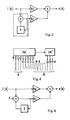
- the structure of the DLF unit described above is designed for the implementation of a second order filter, the basic diagram of which is represented in figure 3.
- the input signal i(n) reaches the storage unit of the filter, therein represented by an adder circuit and a memory element D, and implemented in figure 1 by means of the unit CN 2 .
- the signal i(n) also reaches an element K o designed to effect a multiplication function that is necessary in order to effect the filtering function.
- a second multiplication element is indicated with K, and is connected to the output of the accumulator; the outputs of the elements K o and K, are input into an adder which is implemented in figure 1 by means of the unit FA.
- the invention makes it possible to carry out a further simplification in respect to loops of the known type, in as much as the elements K o and K, are implemented through the counters CN, and CN 2 ; these latter are really made up of just as many counting chains, one of which is shown in the diagram in figure 4.
- Said structure is designed to carry out the multiplication function mentioned above in as much as it includes a first section CN' with N outputs, K of which referring to the least significant bits are neglected.
- Another section CN" with K outputs is cascade connected to the section CN'. It can be shown that the number K of the neglected least significant bits defines the multiplication factor of the filter and in the end the cutoff frequency of the filter.
- the most significant N-K outputs of the section CN' together with the K outputs of the section CN" are input into the adder circuit FA.
- the digital filter DLF can be implemented by means of a microprocessor system pP as is shown in figure 5.
- the unit pP carries out a cycle of operations after each phase measurement carried out by the unit PD (pulses illustrated in diagram 6 of figure 2). Said cycle includes the processing of the binary configuration available on the output of the unit CN, ( ⁇ P carries out the storage function usually carried out by CN 2 within itself), in order to make the numerical (digital) control signal of the DCO unit available.
- Delaying means MR are also shown in figure 1 which are not absolutely essential to the circuit's operation although their presence is in some case advantageous in as much as it gives greater operational stability to the circuit.
- the presence of said means MR is however particularly useful when the DPLL loop is used to make a sequence of timing pulses available that is phase locked to an input signal F, modulated for example according to a code of the two-phase type; said coding forsees sending into the line levels 0-1 when the binary signal has a logical level 0, and sending on levels 1-0 when the binary signal has a logical level 1.
- the abovementioned stability problems are resolved by inserting a multiplier circuit into the ring (see Holly C. Osborne in the aforementioned document-page 1359).
- said unit is not easily implemented so the invention includes the presence of means designed to delay the signal F 2 by means of using particularly simple and economical circuit solutions which are also designed to easily vary the value of the delay.
- the delay of the signal F 2 may easily be obtained by acting on the filtering unit DLF, and in particular on its storage unit which in this case is constituted by the CN 2 unit.
- the said delaying means MR are made up basically by a dividing unit DV (for example of the programmable type), which at the end of each phase comparison decreases the value accumulated by CN 2 by a predetermined number of steps which is in any case linked to the value of delay desired to be obtained.
- a DV unit of the programmable type it is possible to obtain a delay, for example of ⁇ /2, which if required can easily be varied by modifying the programming of the DV unit; furthermore the programmed value remains constant even with the varying of the frequency of the input signal.
- the MR means also include the presence of a D type bistable circuit FF 4 which receives on its timing input the said signal E inverted and has its data input constantly connected to a reference potential. Operation of the DLF unit remains unaltered as far as the carrying out of each phase measurement is concerned (said measurement is taken during each pulse of the sequence E). The decreasing operation described above is started as from the transition "1"->"O" of each pulse of the sequence E, in as much as said transition determines the switching of the FF 4 unit, which in turn qualifies the DV unit to carry out the division of the CK sequence.
- a logical level 0 corresponds to the inverted output of the FF 4 unit, which through a first logical sum unit O 1 , determines qualification for counting of the CN 2 unit (EN signal); furthermore, this latter unit receives on its counting direction control input (U/D signal) the level forseen for counting backwards, through a logical sum unit 0 2 .
- the CN 2 unit decreases its own contents by a value determined by the DV unit; in fact activation of the output of said unit causes the reset of the FF 4 unit which, by means of the O2 unit, qualifies the CN 2 unit during the time in which the output of the EX unit is not active. It can be shown that by decreasing the value accumulated by CN 2 by a predetermined number of steps, we can obtain the effect of delaying the signal F 2 by a value linked to the aforesaid number of steps.
- the basic diagram of the digital filter DLF in figure 3 is modified as illustrated in figure 6.
- the size e indicates the value by, which the contents of the accumulator are decreased and in the end the value of the delay shown by the signal F 2 in respect to F i .
- the loop of this invention is implementable with particularly simple and economical units which do not create any limits in operational speed, excepting those that are typical of the type of technology with which said units have been produced. If the said units are made in ECL technology, the loop is suitable to operate at frequencies in the order of about a hundred MHz. It must be kept in mind that the value of the operating frequency affects the degree of definition of the measurements carried out.
- the loop is designed to measure phase shifts of a value that is not less that the period of the said CK sequence and consequently, the higher the operating frequency is, the higher is the degree of definition. Therefore, by producing the loop with a technology that makes it possible to reach high operation speeds it is possible to carry out measurements with a particularly high degree of definition.
- the value of said operational frequency also influences the jitter associated to the signal F 2 , as well as the abovementioned degree of definition.
- the pulses of the sequence F 2 are in fact subject to jitter, the value of which is a function of the relationship between the frequency of the said CK sequence and the frequency of the input signal (see D'Andrea and Russo-IEEE Transaction on Communication-Vol. Com.
Landscapes
- Stabilization Of Oscillater, Synchronisation, Frequency Synthesizers (AREA)
Description
- The present invention refers to a digital phase locked loop (DPLL) which has a linear type phase characteristic.
- Phase locked loops are mainly used in transmission systems of the synchronous type in order to generate a sequence of timing pulses the frequency of which is locked at the frequency of a reference signal.
- In the past this type of loop (circuit) was made mainly by adopting analog type solutions which, over the last few years have become destined to be substitued by digital type solutions, due especially to the fact that the first sort tend to have problems of calibration, thermal drift, ageing of components and linearity, which are not to be found in the digital type solutions.
- Therefore, digital phase locked loops have been studied and developed which mostly have a phase characteristic of a sinusoidal type.
- This type of loop however, has the inconvenience that the phase error picked up by them is a function, not only of the phase shift between the reference signal and the signal generated locally, but also of the power of the reference signal (input signal). As a consequence, the value of said phase error may appear erroneously altered when the level of the input signal is susceptible to variations. In order to minimize the value of said variations, the said solutions of the type already well known, include the use of a gain controlling amplifier (see Holly C. Osborne-IEEE Transaction on Communication-Vol. Com. 28 No. 8 August 1980-pages 1343-1363) which makes the said reference signal available on the output with a level of a predetermined value and in any case without the aforementioned fluctuations. Said gain controlling amplifier is however an analog type circuit which has the same calibration and drift problems as those illustrated above, and therefore makes the advantages gained from the presence of digital type solutions in the phase locked loop, itself, all in vain.
- In the IEEE magazine Transaction on Communication-Vol. Com. 30 No. 10 October 1982-pages 2398-2411, a digital phase locked loop is illustrated which is therein indicated with the title "Digital Tanlock Loop", which has a phase characteristic of linear type in order to make the loop's operation insensitive to variations in the level of the input signal. However the loop therein described has a linearity field of a limited range (from -n to +n) and its implementation requires the use of sampling circuits or loops and of an analog-digital converter, which in turn has the inconvenience described above with reference to analog sysmems and phase locked loops with sinusoidal type phase characteristics. Furthermore, said type of unit limits the operational speed of the phase locked loop as it is not possible to operate with high frequency signals.
- The aim of the present invention is to produce a digital phase locked loop having a linear phase characteristic in a much wider field (―2n―+2n==4n), without having to use components which present the typical inconvenience of analog components or which introduce limits in operational speed. A further aim is to make the loop's hardware particularly simple as well as implementable in an integrated form.
- US-A-3.715.751 (Mead) describes a digital phase locked loop (DPLL) circuit comprising a phase comparator designed to compare the phase of a reference signal with the phase of the signal generated by a digitally controlled oscillator; digital filtering means receiving the output signal of the phase comparator and providing a digital control signal for the digitally controlled oscillator and said digitally controlled oscillator receiving the digital word generated by the filtering means on its control input and a timing pulses sequence on its counting input.
- Object of the present invention is a digital phase locked loop circuit of the above described type and further comprising counting means inserted between the phase comparator and the digital filtering means, where
- -the phase comparator generates a first output signal expressing the sign of the phase shift and a second pulse output signal whose length is proportional to the value of the phase shift;
- -the counting means, fed by the first and the second output signal of the phase comparator and by the timing pulse sequence, convert into digital form the length of each pulse of the second output signal of the phase compartor; said counting means comprise a first up-down counter which receives the said timing pulses sequence on its counting input, the first output of the phase comparator on its counting direction control input and the second output of the phase comparator on its reset input;
- -the digital filtering means receive also the output of the counting means on their input;
- -the digital control oscillator comprises a presettable counter.
- All the means listed above may be implemented with purely digital units and have no limits in operational speed, excepting those imposed by the type of technology adopted.
- Furthermore, thanks to the use of a phase comparator designed to output both the value and the sign of the shifting, the hardware of the counting means and the filtering means is simplified with respect to the corresponding units used in other known arrangements.
- The above characteristics and some others of the invention may be clarified by the following description which refers to a non-limiting example and is completed with the attached diagrams, in which:
- -figure 1 shows the block diagram of the phase locked loop made according to the invention;
- figure 2 shows wave forms referring to figure 1:
- -figure 3 shows the basic diagram of the digital filter DLF in figure 1;
- -figure 4 shows one way of making the counters CN, or CN2 in figure 1;
- -figure 5 shows another version of the DLF unit in figure 1;
- -figure 6 shows the same diagram as figure 3 but modified in accordance with the presence of the MR means in figure 1.
- The block diagram shown in figure 1 includes a phase detector PD which receives a signal F, constituting the reference signal on its first input, and a signal F2 constituting the signal generated locally on its second input. Said signals reach the timing inputs of their respective D type bistable circuits FF, and FF2, which have their data input continuously connected to a reference potential.
- The outputs from the units FF1 and FF2 are input into an exclusive logical sum unit EX, as well as being input into a logical product unit P. This latter unit has its output connected to the reset input of the FF, and FF2 units. The output from the FF1 unit also comes onto the data input of another D type bistable circuit FF3, which receives the output of the FF2 unit on its timing input.
- In figure 2, diagrams 1 and 2, the said signals F, and F2 are illustrated, and in particular in figure 2a the signal F1 leading on the signal F2 is illustrated, whilst in figure 2b the opposite solution is taken into consideration.
- In diagrams 3 and 4, on the other hand, the waveforms corresponding to the output from the FF, and FF2 units are illustrated, whilst in diagram 5 and 6 the waveforms corresponding respectively to the outputs from the FF3 and EX units are illustrated.
- From an examinatin of the waveforms shown in figure 2a and fiure 2b it becomes evident that a sequence of pulses the duration of which expresses the value of the phase shift between the sequence F1 and the sequence F2 corresponds with the output from the EX unit (diagram 6). Whilst a logical level "0" in the case of the opposite situation occurring (diagram 5b): therefore, the logical level of the FF2 output expresses the sign of the phase shift.
- It is to be noted that the presence of the bistable circuit FF3 can be considered superfluous in the great majority of cases in as much as the information concerning the sign S of the phase shift can be picked up on the output from the FF1 unit.
- The presence of the FF3 unit is necessary solely when the circuits that follow after have a very high operational speed, and in any case that is high enough to pick up the presence of the pulses (very narrow) illustrated in diagram 3 of figure 2b.
- The output from the phase comparator PD is input into counting means CM designed to convert into numerical form each of the pulses of
sequence 6 which corresponds to the output from the EX unit. Thanks to the adoption of a phase comparator PD that provides both the sign and the value of the phase shift the said counting means can be implemented by means of a simple up-down counter CN,; this latter unit receives on its counting input C a sequence of timing pulses CK at very high frequency (in relationship to the frequency of the input signal F,), on its reset input R the output of the EX unit (CN, starts counting, or else is reset, when ths output from the EX unit is active, or else non-active), and on its counting direction control input U/D the output from the FF3 unit (or FF, if FF3 is missing). - In correspondence with each phase comparison carried out by the PD unit, the CN, unit outputs a binary configuration expressiong the value of the phase shift measured. Said configuration is input into the digital filter of the ring DLF which utilizes a particularly simple and economical storage unit. In fact, in order to carry out the aforesaid filtering, it is necessary to store the results from the phase measurements carried out previously, before the one actually being carried out, as well as the algebraical sum of the value measured against the stored value. Thanks to the use of the said PD unit designed to output the phase shift sign, the function described above can easily be implemented by means of a further up-down counter CN2. In the already known sorts of unit, on the other hand, implementation of this function necessitates the use of memory units and of an arithmetical and logical unit ALU which carry out the aforementioned adding and storage functions. The CN2 unit (on the contrary to the CN, unit), is never reset in as much as the output from the EX unit in this case is input into the start counting qualification input EN; therefore, the CN2 unit counts either up, or down, (in relationship to the logical level of the signal S), the pulses of the CK sequence, during the instants in which the pulses output from the EX unit qualify it to start counting. Furthermore, the digital filter also includes an adder circuit FA designed to receive on its input the numbers available on the outputs of the CN1 and CN2 units, as well as to sum said number and input the result to a register RG; this latter memorizes the output of the digital filter during the instants in which deactivation of the EX unit's output is registered. A digital word is available on the output of the RG unit which tends to modify the phase of the locally generated signal until it coincides with that of the reference signal. In fact, the output from the digital filter DLF is input into a digitally controlled oscillator DCO which receives the said sequence of pulses CK and outputs the F2 signal.
- The DCO unit can be implemented by means of a presettable counter which after each phase comparison receives the output signal of the digital filter DLF, automatically presetting itself at the end of each count. As a consequence of this, the DCO unit modifies the phase of the signal corresponding to its own output, in as much as the instant in which its own counting cycle finishes is modified.
- The structure of the DLF unit described above is designed for the implementation of a second order filter, the basic diagram of which is represented in figure 3. In this diagram the input signal i(n) reaches the storage unit of the filter, therein represented by an adder circuit and a memory element D, and implemented in figure 1 by means of the unit CN2. The signal i(n) also reaches an element Ko designed to effect a multiplication function that is necessary in order to effect the filtering function. A second multiplication element is indicated with K, and is connected to the output of the accumulator; the outputs of the elements Ko and K, are input into an adder which is implemented in figure 1 by means of the unit FA.
- It must be noted that the invention makes it possible to carry out a further simplification in respect to loops of the known type, in as much as the elements Ko and K, are implemented through the counters CN, and CN2; these latter are really made up of just as many counting chains, one of which is shown in the diagram in figure 4. Said structure is designed to carry out the multiplication function mentioned above in as much as it includes a first section CN' with N outputs, K of which referring to the least significant bits are neglected. Another section CN" with K outputs is cascade connected to the section CN'. It can be shown that the number K of the neglected least significant bits defines the multiplication factor of the filter and in the end the cutoff frequency of the filter. The most significant N-K outputs of the section CN' together with the K outputs of the section CN" are input into the adder circuit FA.
- Implementation of a first order filter is noticeably simplified with respect to the structure described above in as much as it does not require the units CN2 and FA to be present, and consequently the CN, unit is connected directly to the RG unit. Therefore the invention allows implementation of the multiplication function by means of counting chains which are much simpler and more economical than the multiplication circuits used in the known types of system. On the basis of a further form of realization of the invention, the digital filter DLF can be implemented by means of a microprocessor system pP as is shown in figure 5. The unit pP carries out a cycle of operations after each phase measurement carried out by the unit PD (pulses illustrated in diagram 6 of figure 2). Said cycle includes the processing of the binary configuration available on the output of the unit CN, (µP carries out the storage function usually carried out by CN2 within itself), in order to make the numerical (digital) control signal of the DCO unit available.
- Delaying means MR are also shown in figure 1 which are not absolutely essential to the circuit's operation although their presence is in some case advantageous in as much as it gives greater operational stability to the circuit. The presence of said means MR is however particularly useful when the DPLL loop is used to make a sequence of timing pulses available that is phase locked to an input signal F, modulated for example according to a code of the two-phase type; said coding forsees sending into the line levels 0-1 when the binary signal has a logical level 0, and sending on levels 1-0 when the binary signal has a
logical level 1. In the known types of DPLL loops the abovementioned stability problems are resolved by inserting a multiplier circuit into the ring (see Holly C. Osborne in the aforementioned document-page 1359). However said unit is not easily implemented so the invention includes the presence of means designed to delay the signal F2 by means of using particularly simple and economical circuit solutions which are also designed to easily vary the value of the delay. - According to this invention the delay of the signal F2 may easily be obtained by acting on the filtering unit DLF, and in particular on its storage unit which in this case is constituted by the CN2 unit. The said delaying means MR are made up basically by a dividing unit DV (for example of the programmable type), which at the end of each phase comparison decreases the value accumulated by CN2 by a predetermined number of steps which is in any case linked to the value of delay desired to be obtained. By using a DV unit of the programmable type it is possible to obtain a delay, for example of π/2, which if required can easily be varied by modifying the programming of the DV unit; furthermore the programmed value remains constant even with the varying of the frequency of the input signal. The MR means also include the presence of a D type bistable circuit FF4 which receives on its timing input the said signal E inverted and has its data input constantly connected to a reference potential. Operation of the DLF unit remains unaltered as far as the carrying out of each phase measurement is concerned (said measurement is taken during each pulse of the sequence E). The decreasing operation described above is started as from the transition "1"->"O" of each pulse of the sequence E, in as much as said transition determines the switching of the FF4 unit, which in turn qualifies the DV unit to carry out the division of the CK sequence.
- A logical level 0 corresponds to the inverted output of the FF4 unit, which through a first logical sum unit O1, determines qualification for counting of the CN2 unit (EN signal); furthermore, this latter unit receives on its counting direction control input (U/D signal) the level forseen for counting backwards, through a logical sum unit 02.
- Therefore the CN2 unit decreases its own contents by a value determined by the DV unit; in fact activation of the output of said unit causes the reset of the FF4 unit which, by means of the O2 unit, qualifies the CN2 unit during the time in which the output of the EX unit is not active. It can be shown that by decreasing the value accumulated by CN2 by a predetermined number of steps, we can obtain the effect of delaying the signal F2 by a value linked to the aforesaid number of steps.
- By completing the phase locked loop with the delaying means described above, the basic diagram of the digital filter DLF in figure 3 is modified as illustrated in figure 6. In said figure the size e indicates the value by, which the contents of the accumulator are decreased and in the end the value of the delay shown by the signal F2 in respect to Fi. Following up all that has been described above, it soon becomes evident that the loop of this invention is implementable with particularly simple and economical units which do not create any limits in operational speed, excepting those that are typical of the type of technology with which said units have been produced. If the said units are made in ECL technology, the loop is suitable to operate at frequencies in the order of about a hundred MHz. It must be kept in mind that the value of the operating frequency affects the degree of definition of the measurements carried out. In fact the loop is designed to measure phase shifts of a value that is not less that the period of the said CK sequence and consequently, the higher the operating frequency is, the higher is the degree of definition. Therefore, by producing the loop with a technology that makes it possible to reach high operation speeds it is possible to carry out measurements with a particularly high degree of definition. It must also be borne in mind that the value of said operational frequency, also influences the jitter associated to the signal F2, as well as the abovementioned degree of definition. The pulses of the sequence F2 are in fact subject to jitter, the value of which is a function of the relationship between the frequency of the said CK sequence and the frequency of the input signal (see D'Andrea and Russo-IEEE Transaction on Communication-Vol. Com. 26-No. 9, September 1978-pages1355-1364). For example, by adopting a CK signal with a frequency of 1024 KHz and an input signal with a frequency of 4 KHz, the result is that the jitter associated to the pulses of the F2 sequence is of about 2.8 degrees. Therefore by adopting an operating frequency of a high value it is possible to obtain a jitter of the value described above, the negative effects of which may be considered negligible. Furthermore, the loop has a linear phase characteristic in a particularly wide field (from +2nto +2n=4n), in accordance with the established purpose of the invention.
- It is possible, without overstepping the limits of the invention, to connect a digital analog convertor to the output of the DLF unit (not illustrated), and substitute the DCO unit with a voltage controlled unit. This latter implementation can be useful when the F2 signal must have a high frequency.
Claims (9)
characterized by the fact that it comprises counting means (CM) inserted between the phase comparator (PD) and the digital filtering means (DLF); and by the fact that
Applications Claiming Priority (2)
| Application Number | Priority Date | Filing Date | Title |
|---|---|---|---|
| IT2434783 | 1983-12-23 | ||
| IT24347/83A IT1194538B (en) | 1983-12-23 | 1983-12-23 | NUMERIC CIRCUIT WITH PHASE HOOK (PDLL) |
Publications (3)
| Publication Number | Publication Date |
|---|---|
| EP0148525A2 EP0148525A2 (en) | 1985-07-17 |
| EP0148525A3 EP0148525A3 (en) | 1987-08-19 |
| EP0148525B1 true EP0148525B1 (en) | 1990-05-23 |
Family
ID=11213199
Family Applications (1)
| Application Number | Title | Priority Date | Filing Date |
|---|---|---|---|
| EP84201795A Expired EP0148525B1 (en) | 1983-12-23 | 1984-12-04 | Digital phase locked loop (dpll) |
Country Status (4)
| Country | Link |
|---|---|
| US (1) | US4596964A (en) |
| EP (1) | EP0148525B1 (en) |
| DE (2) | DE3482361D1 (en) |
| IT (1) | IT1194538B (en) |
Cited By (1)
| Publication number | Priority date | Publication date | Assignee | Title |
|---|---|---|---|---|
| US11595048B1 (en) * | 2022-03-25 | 2023-02-28 | Cypress Semiconductor Corporation | Faster phase-locked loop locking using successive approximation toward a target frequency |
Families Citing this family (8)
| Publication number | Priority date | Publication date | Assignee | Title |
|---|---|---|---|---|
| US4715000A (en) * | 1985-08-06 | 1987-12-22 | General Electric Company | Digital phase-locked loop and frequency measuring device |
| US4787096A (en) * | 1987-03-04 | 1988-11-22 | National Semiconductor Corp. | Second-order carrier/symbol sychronizer |
| EP0310088B1 (en) * | 1987-10-01 | 1996-06-05 | Sharp Kabushiki Kaisha | Digital phase-locked loop system |
| DE4004195C2 (en) * | 1990-02-12 | 1996-10-02 | Broadcast Television Syst | Circuit arrangement for generating a signal coupled to a reference signal |
| US5442315A (en) * | 1993-07-27 | 1995-08-15 | International Business Machines Corporation | Bit stream rate asynchronous digital phase-locked loop |
| DE19653129C2 (en) * | 1996-12-19 | 1999-01-28 | Siemens Ag | Method for generating a drive signal for a voltage-controlled oscillator in a phase locked loop |
| US6249159B1 (en) * | 1999-12-30 | 2001-06-19 | Intel Corporation | Frequency control circuit having increased control bandwidth at lower device operating speed |
| FR2854751B1 (en) * | 2003-05-07 | 2005-07-22 | St Microelectronics Sa | CLOCK RECOVERY CIRCUIT |
Family Cites Families (5)
| Publication number | Priority date | Publication date | Assignee | Title |
|---|---|---|---|---|
| US3562661A (en) * | 1969-01-15 | 1971-02-09 | Ibm | Digital automatic phase and frequency control system |
| US3715751A (en) * | 1970-09-30 | 1973-02-06 | Raytheon Co | Digital speed gate for doppler radar |
| US3883817A (en) * | 1973-08-20 | 1975-05-13 | Nasa | Digital phase-locked loop |
| US4019153A (en) * | 1974-10-07 | 1977-04-19 | The Charles Stark Draper Laboratory, Inc. | Digital phase-locked loop filter |
| US4531102A (en) * | 1983-02-28 | 1985-07-23 | Gk Technologies, Incorporated | Digital phase lock loop system |
-
1983
- 1983-12-23 IT IT24347/83A patent/IT1194538B/en active
-
1984
- 1984-12-04 DE DE8484201795T patent/DE3482361D1/en not_active Expired - Lifetime
- 1984-12-04 EP EP84201795A patent/EP0148525B1/en not_active Expired
- 1984-12-04 DE DE198484201795T patent/DE148525T1/en active Pending
- 1984-12-20 US US06/684,045 patent/US4596964A/en not_active Expired - Fee Related
Cited By (1)
| Publication number | Priority date | Publication date | Assignee | Title |
|---|---|---|---|---|
| US11595048B1 (en) * | 2022-03-25 | 2023-02-28 | Cypress Semiconductor Corporation | Faster phase-locked loop locking using successive approximation toward a target frequency |
Also Published As
| Publication number | Publication date |
|---|---|
| IT1194538B (en) | 1988-09-22 |
| EP0148525A3 (en) | 1987-08-19 |
| DE148525T1 (en) | 1985-09-26 |
| DE3482361D1 (en) | 1990-06-28 |
| US4596964A (en) | 1986-06-24 |
| EP0148525A2 (en) | 1985-07-17 |
| IT8324347A0 (en) | 1983-12-23 |
Similar Documents
| Publication | Publication Date | Title |
|---|---|---|
| US5757238A (en) | Fast locking variable frequency phase-locked loop | |
| US4030045A (en) | Digital double differential phase-locked loop | |
| US4764737A (en) | Frequency synthesizer having digital phase detector with optimal steering and level-type lock indication | |
| US5059979A (en) | Digital control circuit for tuning systems with a pulse density modulation digital to analog converter | |
| GB2180708A (en) | Phase-comparator lock-detect circuit for a frequency synthesiser | |
| CA1054232A (en) | Phase detector having a 360.degree. linear range for periodic and aperiodic input pulse streams | |
| US5635875A (en) | PLL circuit with improved stability | |
| US4204173A (en) | Tuning circuit with provisions for reducing pulse width jitter | |
| US4596964A (en) | Digital phase locked loop | |
| GB2041682A (en) | Digital frequency lock tuning system | |
| EP0588656B1 (en) | Digital signal-edge time measurement circuit | |
| US6111471A (en) | Apparatus and method for setting VCO free-running frequency | |
| US5896428A (en) | Digital counter and digital phase locked loop circuit using same | |
| US4916403A (en) | Digital phase-locked loop system | |
| US4878231A (en) | N-PI phase/frequency detector | |
| GB2205012A (en) | Digital phase-locked loop circuits | |
| EP0164785B1 (en) | Electric circuit arrangement comprising a phase control-circuit | |
| EP0435552B1 (en) | A phase locked loop with reduced frequency/phase lock time | |
| US6229864B1 (en) | Phase locked loop lock condition detector | |
| US5563531A (en) | Digital phase comparator | |
| EP0005128A2 (en) | Improvement in circuits for the automatic tuning of voltage controlled filters | |
| US4573024A (en) | PLL having two-frequency VCO | |
| USRE32686E (en) | Digital frequency lock tuning system | |
| RU2119717C1 (en) | Device for phase synchronization | |
| US6593815B2 (en) | Full digital phase locked loop and circuitry for utilizing the same |
Legal Events
| Date | Code | Title | Description |
|---|---|---|---|
| PUAI | Public reference made under article 153(3) epc to a published international application that has entered the european phase |
Free format text: ORIGINAL CODE: 0009012 |
|
| AK | Designated contracting states |
Designated state(s): DE FR GB NL SE |
|
| TCNL | Nl: translation of patent claims filed | ||
| EL | Fr: translation of claims filed | ||
| DET | De: translation of patent claims | ||
| PUAL | Search report despatched |
Free format text: ORIGINAL CODE: 0009013 |
|
| AK | Designated contracting states |
Kind code of ref document: A3 Designated state(s): DE FR GB NL SE |
|
| 17P | Request for examination filed |
Effective date: 19880129 |
|
| 17Q | First examination report despatched |
Effective date: 19881223 |
|
| GRAA | (expected) grant |
Free format text: ORIGINAL CODE: 0009210 |
|
| AK | Designated contracting states |
Kind code of ref document: B1 Designated state(s): DE FR GB NL SE |
|
| PG25 | Lapsed in a contracting state [announced via postgrant information from national office to epo] |
Ref country code: SE Effective date: 19900523 Ref country code: NL Effective date: 19900523 |
|
| REF | Corresponds to: |
Ref document number: 3482361 Country of ref document: DE Date of ref document: 19900628 |
|
| ET | Fr: translation filed | ||
| NLV1 | Nl: lapsed or annulled due to failure to fulfill the requirements of art. 29p and 29m of the patents act | ||
| PLBE | No opposition filed within time limit |
Free format text: ORIGINAL CODE: 0009261 |
|
| STAA | Information on the status of an ep patent application or granted ep patent |
Free format text: STATUS: NO OPPOSITION FILED WITHIN TIME LIMIT |
|
| 26N | No opposition filed | ||
| PGFP | Annual fee paid to national office [announced via postgrant information from national office to epo] |
Ref country code: GB Payment date: 19921120 Year of fee payment: 9 |
|
| PGFP | Annual fee paid to national office [announced via postgrant information from national office to epo] |
Ref country code: DE Payment date: 19930226 Year of fee payment: 9 |
|
| PG25 | Lapsed in a contracting state [announced via postgrant information from national office to epo] |
Ref country code: GB Effective date: 19931204 |
|
| PGFP | Annual fee paid to national office [announced via postgrant information from national office to epo] |
Ref country code: FR Payment date: 19931230 Year of fee payment: 10 |
|
| GBPC | Gb: european patent ceased through non-payment of renewal fee |
Effective date: 19931204 |
|
| PG25 | Lapsed in a contracting state [announced via postgrant information from national office to epo] |
Ref country code: DE Effective date: 19940901 |
|
| PG25 | Lapsed in a contracting state [announced via postgrant information from national office to epo] |
Ref country code: FR Effective date: 19950831 |
|
| REG | Reference to a national code |
Ref country code: FR Ref legal event code: ST |