EP0147490B1 - Power supply input system - Google Patents
Power supply input system Download PDFInfo
- Publication number
- EP0147490B1 EP0147490B1 EP19830307698 EP83307698A EP0147490B1 EP 0147490 B1 EP0147490 B1 EP 0147490B1 EP 19830307698 EP19830307698 EP 19830307698 EP 83307698 A EP83307698 A EP 83307698A EP 0147490 B1 EP0147490 B1 EP 0147490B1
- Authority
- EP
- European Patent Office
- Prior art keywords
- input
- voltage
- power supply
- circuit
- mains
- Prior art date
- Legal status (The legal status is an assumption and is not a legal conclusion. Google has not performed a legal analysis and makes no representation as to the accuracy of the status listed.)
- Expired
Links
- 238000012544 monitoring process Methods 0.000 claims description 3
- 230000002457 bidirectional effect Effects 0.000 claims description 2
- 239000003990 capacitor Substances 0.000 description 8
- 238000000034 method Methods 0.000 description 6
- 238000010304 firing Methods 0.000 description 3
- 238000009434 installation Methods 0.000 description 2
- 238000004519 manufacturing process Methods 0.000 description 2
- 230000001276 controlling effect Effects 0.000 description 1
- 230000001105 regulatory effect Effects 0.000 description 1
- 230000001360 synchronised effect Effects 0.000 description 1
- 238000004804 winding Methods 0.000 description 1
Images
Classifications
-
- H—ELECTRICITY
- H02—GENERATION; CONVERSION OR DISTRIBUTION OF ELECTRIC POWER
- H02M—APPARATUS FOR CONVERSION BETWEEN AC AND AC, BETWEEN AC AND DC, OR BETWEEN DC AND DC, AND FOR USE WITH MAINS OR SIMILAR POWER SUPPLY SYSTEMS; CONVERSION OF DC OR AC INPUT POWER INTO SURGE OUTPUT POWER; CONTROL OR REGULATION THEREOF
- H02M5/00—Conversion of AC power input into AC power output, e.g. for change of voltage, for change of frequency, for change of number of phases
- H02M5/02—Conversion of AC power input into AC power output, e.g. for change of voltage, for change of frequency, for change of number of phases without intermediate conversion into DC
- H02M5/04—Conversion of AC power input into AC power output, e.g. for change of voltage, for change of frequency, for change of number of phases without intermediate conversion into DC by static converters
- H02M5/22—Conversion of AC power input into AC power output, e.g. for change of voltage, for change of frequency, for change of number of phases without intermediate conversion into DC by static converters using discharge tubes with control electrode or semiconductor devices with control electrode
- H02M5/25—Conversion of AC power input into AC power output, e.g. for change of voltage, for change of frequency, for change of number of phases without intermediate conversion into DC by static converters using discharge tubes with control electrode or semiconductor devices with control electrode using devices of a thyratron or thyristor type requiring extinguishing means
- H02M5/257—Conversion of AC power input into AC power output, e.g. for change of voltage, for change of frequency, for change of number of phases without intermediate conversion into DC by static converters using discharge tubes with control electrode or semiconductor devices with control electrode using devices of a thyratron or thyristor type requiring extinguishing means using semiconductor devices only
- H02M5/2573—Conversion of AC power input into AC power output, e.g. for change of voltage, for change of frequency, for change of number of phases without intermediate conversion into DC by static converters using discharge tubes with control electrode or semiconductor devices with control electrode using devices of a thyratron or thyristor type requiring extinguishing means using semiconductor devices only with control circuit
Definitions
- This invention relates to a system for controlling the input voltage to a switch mode power supply.
- a system with the features of the precharacterizing part of claim 1 is known from EP-Al-21714.
- a motor drive comprises an electronic switch connected in series with a universal motor across an a.c. supply (LM), and the switch is activated in timed relationship with the supply frequency by a feedback control system incorporating logic for predetermining the speed/ torque characteristic of the drive by delivering an error signal to adjust the timed relationship at which the electronic switch is activated according to the relative magnitudes of motor voltage V s and current ' s .
- the logic may be hard wired or within a preprogrammed microprocessor.
- a power supply input system for connection of a switch mode power supply to AC mains and in which a bidirectional triode thyristor (TRIAC) is connected in series with a voltage doubler circuit
- the system comprising a control circuit including a comparator circuit which receives inputs from the voltage doubler circuit and a timing ramp generator, and a zero crossing detector which monitors the mains input and provides an input to the timing ramp generator
- the system further comprises under-voltage and over-current monitoring circuits which provide an input to a reset circuit which provides an input to the timing ramp generator to select the slope of the waveform generated, so that at the time of application of power the conduction angle is zero and slowly increases to that demanded by the control circuit.
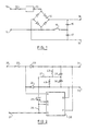
- Fig. 1 shows a prior art voltage doubler circuit which is configured for 110 v or 240 v by the omission or installation of a link.
- the AC mains input is applied across terminals 10 and 11, a fuse 12 and a surge current limiting device 13, which may be a resistor, thermistor, or resistor plus triac, are connected in series from terminal 10 to one arm of a bridge circuit 14.
- Terminal 11 is connected to the opposite arm of the bridge and through a configuring link 15 to the centre of two power supply capacitors 16 and 17.
- the DC output which may be fed to a switching stage is taken from terminals 18 and 19.
- Fig. 2 shows a preferred embodiment of the invention which maintains a constant DC voltage across the power input capacitors regardless of the mains voltage between limits of 80 v to 300 v (say). This is achieved by placing a TRIAC 25 in series with the mains input 20, 21 to the power supply. The conduction angle of the TRIAC is varied cycle by cycle to maintain a constant DC voltage across the input capacitors 29, 30 which is conjunction with diodes 23, 24 form a voltage doubler circuit.
- the conduction angle of the TRIAC is controlled by firing pulses provided by a control circuit 28.
- the control circuit compares the DC voltage across the power supply input capacitors 29, 30 to a reference voltage and produces an error term which determines the phase delay between a mains input zero crossing and the production of a firing pulse.
- Resistors 42 and 43 ensure equal voltages are present across capacitors 29 and 30 and provide a discharge path when the mains input is removed from the power supply.
- the control circuit 28 (which is shown in more detail in Fig. 3) ensures that at power on time the conduction angle of the TRIAC is zero and that this then slowly increases to provide the correct DC voltage across capacitors 29, 30 and the DC output terminals 31, 32 which are connected to a switching stage. By using this technique the problem of excessive inrush current normally associated with switched mode power supplies is eliminated.
- Resistor 26 senses the current flowing through the TRIAC and provides an input to the control circuit 28 to enable the monitoring of the current being taken by the power supply (during both power up and normal operation) and vary the conduction angle if a fault condition is detected.
- Resistor 27 provides a "softening" of the cycle by cycle current and a degree of limiting under major fault conditions.
- the fuse 22 provides protection against fire hazards during major fault conditions.
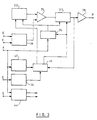
- Fig. 3 shows the control circuit 28 in more detail.
- a timing ramp generator 33 generates a ramp waveform which is synchronised to mains voltage zero crossings by a zero crossing detector 34. This ramp waveform forms the reference input to a comparator 35.
- the DC bus voltage of the power supply is applied to a differential-to-single-ended converter 36 the output of which is the second comparator input.
- a pulse timing circuit 37 is enabled and produces firing pulses which are applied to the gate of the TRIAC through an amplifier 38.
- the gain and sense of the circuitry is such as to provide a stable self-regulating feedback system.
- the ramp generator 33 produces ramps with a very low slope angle allowing only very small conduction angles and hence no inrush of current. Once the correct DC bus voltage has been reached the ramp generator is switched to produce steep angled ramp waveforms to allow a full range of conduction angle control.
- the reset circuitry 41 resets the ramp generator 33, the zero crossing detector 34 and the pulse timing circuit 37 to initial power on conditions and the circuitry then soft starts as at initial power on time.
- a voltage regulator circuit 44 provides a regulated DC voltage for use by the control circuitry shown in Fig. 3.
- Input D is the ground reference.
Landscapes
- Engineering & Computer Science (AREA)
- Power Engineering (AREA)
- Rectifiers (AREA)
Description
- This invention relates to a system for controlling the input voltage to a switch mode power supply. A system with the features of the precharacterizing part of claim 1 is known from EP-Al-21714.
- Conventionally switched mode power supplies are built with an input stage which can either be configured as a full wave bridge circuit or as a voltage doubler by the omission or installation of a link. This entails either manufacturing two power supply parts or one part with a voltage selection panel or switch with the attendant problems of cost and wrong selection.
- Prior art switched mode power supplies approach the problem of inrush current limiting in one of four ways. The best of these can perhaps reduce the peak inrush current of a 110 volt power supply to around 40 amps peak. Naturally this high peak current leads to expensive (or short lived) mains switches and to large stresses within the power supply input circuitry. The four techniques may be summarised as:
- 1. No specific limiting components, this relies on the ESR of the input capacitors and the forward impedance of the diodes to limit the charging current-this is generally not considered acceptable in professional equipment.
- 2. A fixed resistor in series with the input, this provides a degree of limiting but is wasteful of power when the supply is operating normally and is unreliable because of its high running temperature.
- 3. A resistor with a negative temperature coefficient in series with the input, this can be designed to give better limiting when switching on from cold than the earlier techniques but is totally ineffective when switching off and then on again so that the capacitors have discharged but the thermistor has not cooled down.
- 4. A fixed resistor in series with the input which is shoirt circuited by a TRIAC once the supply is operating normally, this is the best of the available techniques but requires a feedback winding on the switching transformer and does not eliminate inrush current it simply limits it to around 40 amps (eg).
- The use of phase control techniques is well known. UK
Patents Application 2 058 405 A (Con- trology Techniques Limited) describes motor drive circuitry which controls speed and torque using phase control. A motor drive comprises an electronic switch connected in series with a universal motor across an a.c. supply (LM), and the switch is activated in timed relationship with the supply frequency by a feedback control system incorporating logic for predetermining the speed/ torque characteristic of the drive by delivering an error signal to adjust the timed relationship at which the electronic switch is activated according to the relative magnitudes of motor voltage Vs and current 's. The logic may be hard wired or within a preprogrammed microprocessor. - According to the present invention there is provided a power supply input system for connection of a switch mode power supply to AC mains and in which a bidirectional triode thyristor (TRIAC) is connected in series with a voltage doubler circuit, the system comprising a control circuit including a comparator circuit which receives inputs from the voltage doubler circuit and a timing ramp generator, and a zero crossing detector which monitors the mains input and provides an input to the timing ramp generator characterized in that the system further comprises under-voltage and over-current monitoring circuits which provide an input to a reset circuit which provides an input to the timing ramp generator to select the slope of the waveform generated, so that at the time of application of power the conduction angle is zero and slowly increases to that demanded by the control circuit.
- The advantages of the invention over the prior art are switch on inrush current is eliminated rather than simply limited as in conventional designs, this leads to greater reliability and cheaper mains switches, the tolerance of a power supply to mains disturbances and fluctuations is increased because of the extra stage of regulation; the value of protection fuse need not be changed to suit the input voltage as electronic overcurrent protection is inherent in the circuit.
- In order that the invention may be fully understood a preferred embodiment thereof will now be described with reference to the accompanying drawings in which:
- Fig. 1 illustrates a prior art circuit.
- Fig. 2 illustrates the preferred embodiment of the invention.
- Fig. 3 is a block schematic of the control circuit of Fig. 2.
- Referring now to Fig. 1 which shows a prior art voltage doubler circuit which is configured for 110 v or 240 v by the omission or installation of a link. The AC mains input is applied across
terminals device 13, which may be a resistor, thermistor, or resistor plus triac, are connected in series fromterminal 10 to one arm of abridge circuit 14.Terminal 11 is connected to the opposite arm of the bridge and through a configuringlink 15 to the centre of twopower supply capacitors terminals - Fig. 2 shows a preferred embodiment of the invention which maintains a constant DC voltage across the power input capacitors regardless of the mains voltage between limits of 80 v to 300 v (say). This is achieved by placing a TRIAC 25 in series with the
mains input input capacitors 29, 30 which is conjunction withdiodes - The conduction angle of the TRIAC is controlled by firing pulses provided by a
control circuit 28. The control circuit compares the DC voltage across the powersupply input capacitors 29, 30 to a reference voltage and produces an error term which determines the phase delay between a mains input zero crossing and the production of a firing pulse. -
Resistors 42 and 43 ensure equal voltages are present acrosscapacitors 29 and 30 and provide a discharge path when the mains input is removed from the power supply. - The control circuit 28 (which is shown in more detail in Fig. 3) ensures that at power on time the conduction angle of the TRIAC is zero and that this then slowly increases to provide the correct DC voltage across
capacitors 29, 30 and theDC output terminals 31, 32 which are connected to a switching stage. By using this technique the problem of excessive inrush current normally associated with switched mode power supplies is eliminated. -
Resistor 26 senses the current flowing through the TRIAC and provides an input to thecontrol circuit 28 to enable the monitoring of the current being taken by the power supply (during both power up and normal operation) and vary the conduction angle if a fault condition is detected. - Resistor 27 provides a "softening" of the cycle by cycle current and a degree of limiting under major fault conditions. The
fuse 22 provides protection against fire hazards during major fault conditions. - Fig. 3 shows the
control circuit 28 in more detail. Atiming ramp generator 33 generates a ramp waveform which is synchronised to mains voltage zero crossings by a zerocrossing detector 34. This ramp waveform forms the reference input to acomparator 35. - The DC bus voltage of the power supply is applied to a differential-to-single-
ended converter 36 the output of which is the second comparator input. When the comparator output is high apulse timing circuit 37 is enabled and produces firing pulses which are applied to the gate of the TRIAC through anamplifier 38. The gain and sense of the circuitry is such as to provide a stable self-regulating feedback system. - On the initial power application to the circuit the
ramp generator 33 produces ramps with a very low slope angle allowing only very small conduction angles and hence no inrush of current. Once the correct DC bus voltage has been reached the ramp generator is switched to produce steep angled ramp waveforms to allow a full range of conduction angle control. - If an under-voltage or over-current situation is detected by an over-current
monitor 39 or avoltage monitor 40 then thereset circuitry 41 resets theramp generator 33, the zerocrossing detector 34 and thepulse timing circuit 37 to initial power on conditions and the circuitry then soft starts as at initial power on time. - A
voltage regulator circuit 44 provides a regulated DC voltage for use by the control circuitry shown in Fig. 3. Input D is the ground reference.
Claims (2)
Priority Applications (3)
| Application Number | Priority Date | Filing Date | Title |
|---|---|---|---|
| EP19830307698 EP0147490B1 (en) | 1983-12-19 | 1983-12-19 | Power supply input system |
| DE8383307698T DE3379251D1 (en) | 1983-12-19 | 1983-12-19 | Power supply input system |
| JP24258084A JPS60131075A (en) | 1983-12-19 | 1984-11-19 | Power source input device |
Applications Claiming Priority (1)
| Application Number | Priority Date | Filing Date | Title |
|---|---|---|---|
| EP19830307698 EP0147490B1 (en) | 1983-12-19 | 1983-12-19 | Power supply input system |
Publications (2)
| Publication Number | Publication Date |
|---|---|
| EP0147490A1 EP0147490A1 (en) | 1985-07-10 |
| EP0147490B1 true EP0147490B1 (en) | 1989-02-22 |
Family
ID=8191368
Family Applications (1)
| Application Number | Title | Priority Date | Filing Date |
|---|---|---|---|
| EP19830307698 Expired EP0147490B1 (en) | 1983-12-19 | 1983-12-19 | Power supply input system |
Country Status (3)
| Country | Link |
|---|---|
| EP (1) | EP0147490B1 (en) |
| JP (1) | JPS60131075A (en) |
| DE (1) | DE3379251D1 (en) |
Families Citing this family (2)
| Publication number | Priority date | Publication date | Assignee | Title |
|---|---|---|---|---|
| KR930001548A (en) * | 1991-06-13 | 1993-01-16 | 강진구 | Capacitor Input Rectifier Smoothers with Inrush Current Protection |
| CN108155812B (en) * | 2018-01-16 | 2024-03-19 | 深圳市赛格瑞电子有限公司 | Alternating current conversion circuit |
Family Cites Families (3)
| Publication number | Priority date | Publication date | Assignee | Title |
|---|---|---|---|---|
| JPS5232556A (en) * | 1975-09-05 | 1977-03-11 | Toshiba Corp | Supply control device |
| US4268899A (en) * | 1979-06-15 | 1981-05-19 | Sperry Corporation | Bridge-doubler rectifier |
| JPS56111920A (en) * | 1980-02-07 | 1981-09-04 | Olympus Optical Co Ltd | Electric power supply device for flash discharge tube |
-
1983
- 1983-12-19 EP EP19830307698 patent/EP0147490B1/en not_active Expired
- 1983-12-19 DE DE8383307698T patent/DE3379251D1/en not_active Expired
-
1984
- 1984-11-19 JP JP24258084A patent/JPS60131075A/en active Pending
Also Published As
| Publication number | Publication date |
|---|---|
| DE3379251D1 (en) | 1989-03-30 |
| JPS60131075A (en) | 1985-07-12 |
| EP0147490A1 (en) | 1985-07-10 |
Similar Documents
| Publication | Publication Date | Title |
|---|---|---|
| US6038155A (en) | Three phase SCR rectifier bridge with soft start control IC | |
| US5302858A (en) | Method and apparatus for providing battery charging in a backup power system | |
| US6862201B2 (en) | Method and circuitry for active inrush current limiter and power factor control | |
| CN101040570B (en) | A method for reducing load jitter | |
| US5428267A (en) | Regulated DC power supply | |
| US20060022648A1 (en) | Method and control circuitry for improved-performance switch-mode converters | |
| US7088078B2 (en) | Soft-start circuit for power converters | |
| US6493245B1 (en) | Inrush current control for AC to DC converters | |
| EP3068023B1 (en) | Inrush limiter for motor drive ac/ac power converters | |
| JPS60101620A (en) | Antiphase control power switching circuit and method | |
| JP2002538587A (en) | Resonant frequency induction furnace system using capacitive voltage division | |
| JPH02228298A (en) | Power circuit for voltage regulator of generator and method of generating field current | |
| US6307352B1 (en) | High energy charge and depolarization pulse conditioner for an enhanced-reliability lead-acid battery charger | |
| US5801933A (en) | High efficiency voltage converter and regulator circuit | |
| US5393954A (en) | Plasma torch with power supply for equalizing wear to prolong the lifespan of an electrode of the torch | |
| EP0147490B1 (en) | Power supply input system | |
| US4672301A (en) | Power controller circuit with automatic correction for phase lag between voltage and current | |
| EP0732002B1 (en) | Rectifier bridge apparatus | |
| US5737163A (en) | DC-AC converter protection | |
| KR100501694B1 (en) | The power supply apparatus and the method which equips fully a sparc prevention function | |
| JPS5815478A (en) | Current control device in speed control device of dc motor | |
| USRE33184E (en) | Power controller circuit with automatic correction for phase lag between voltage and current | |
| JPH1127933A (en) | Method and device for controlling output of electric consumption body | |
| JP3038800B2 (en) | Switching power supply circuit | |
| JPH08221141A (en) | Power supply circuit |
Legal Events
| Date | Code | Title | Description |
|---|---|---|---|
| PUAI | Public reference made under article 153(3) epc to a published international application that has entered the european phase |
Free format text: ORIGINAL CODE: 0009012 |
|
| 17P | Request for examination filed |
Effective date: 19841214 |
|
| AK | Designated contracting states |
Designated state(s): DE FR GB IT NL SE |
|
| 16A | New documents despatched to applicant after publication of the search report | ||
| 17Q | First examination report despatched |
Effective date: 19860403 |
|
| R17C | First examination report despatched (corrected) |
Effective date: 19870205 |
|
| GRAA | (expected) grant |
Free format text: ORIGINAL CODE: 0009210 |
|
| AK | Designated contracting states |
Kind code of ref document: B1 Designated state(s): DE FR GB IT NL SE |
|
| PG25 | Lapsed in a contracting state [announced via postgrant information from national office to epo] |
Ref country code: SE Effective date: 19890222 Ref country code: NL Effective date: 19890222 Ref country code: IT Free format text: LAPSE BECAUSE OF FAILURE TO SUBMIT A TRANSLATION OF THE DESCRIPTION OR TO PAY THE FEE WITHIN THE PRESCRIBED TIME-LIMIT;WARNING: LAPSES OF ITALIAN PATENTS WITH EFFECTIVE DATE BEFORE 2007 MAY HAVE OCCURRED AT ANY TIME BEFORE 2007. THE CORRECT EFFECTIVE DATE MAY BE DIFFERENT FROM THE ONE RECORDED. Effective date: 19890222 |
|
| REF | Corresponds to: |
Ref document number: 3379251 Country of ref document: DE Date of ref document: 19890330 |
|
| ET | Fr: translation filed | ||
| NLV1 | Nl: lapsed or annulled due to failure to fulfill the requirements of art. 29p and 29m of the patents act | ||
| PLBE | No opposition filed within time limit |
Free format text: ORIGINAL CODE: 0009261 |
|
| STAA | Information on the status of an ep patent application or granted ep patent |
Free format text: STATUS: NO OPPOSITION FILED WITHIN TIME LIMIT |
|
| 26N | No opposition filed | ||
| PGFP | Annual fee paid to national office [announced via postgrant information from national office to epo] |
Ref country code: GB Payment date: 19911111 Year of fee payment: 9 |
|
| PGFP | Annual fee paid to national office [announced via postgrant information from national office to epo] |
Ref country code: FR Payment date: 19911127 Year of fee payment: 9 |
|
| PGFP | Annual fee paid to national office [announced via postgrant information from national office to epo] |
Ref country code: DE Payment date: 19911221 Year of fee payment: 9 |
|
| PG25 | Lapsed in a contracting state [announced via postgrant information from national office to epo] |
Ref country code: GB Effective date: 19921219 |
|
| GBPC | Gb: european patent ceased through non-payment of renewal fee |
Effective date: 19921219 |
|
| PG25 | Lapsed in a contracting state [announced via postgrant information from national office to epo] |
Ref country code: FR Effective date: 19930831 |
|
| PG25 | Lapsed in a contracting state [announced via postgrant information from national office to epo] |
Ref country code: DE Effective date: 19930901 |
|
| REG | Reference to a national code |
Ref country code: FR Ref legal event code: ST |