EP0146594B1 - Verfahren und vorrichtung zum erzeugen von vektorattributen - Google Patents
Verfahren und vorrichtung zum erzeugen von vektorattributen Download PDFInfo
- Publication number
- EP0146594B1 EP0146594B1 EP19840902290 EP84902290A EP0146594B1 EP 0146594 B1 EP0146594 B1 EP 0146594B1 EP 19840902290 EP19840902290 EP 19840902290 EP 84902290 A EP84902290 A EP 84902290A EP 0146594 B1 EP0146594 B1 EP 0146594B1
- Authority
- EP
- European Patent Office
- Prior art keywords
- address
- refresh memory
- attribute
- vector
- starting address
- Prior art date
- Legal status (The legal status is an assumption and is not a legal conclusion. Google has not performed a legal analysis and makes no representation as to the accuracy of the status listed.)
- Expired
Links
- 238000000034 method Methods 0.000 title claims abstract description 12
- 239000013598 vector Substances 0.000 title claims description 56
- 230000015654 memory Effects 0.000 claims abstract description 61
- 230000000007 visual effect Effects 0.000 claims description 15
- 239000011159 matrix material Substances 0.000 claims 2
- 230000004044 response Effects 0.000 description 6
- 230000004048 modification Effects 0.000 description 4
- 238000012986 modification Methods 0.000 description 4
- 241000233805 Phoenix Species 0.000 description 2
- 230000008859 change Effects 0.000 description 2
- 230000006870 function Effects 0.000 description 2
- 230000014509 gene expression Effects 0.000 description 2
- 239000003086 colorant Substances 0.000 description 1
- 238000010586 diagram Methods 0.000 description 1
- 230000000737 periodic effect Effects 0.000 description 1
Images


Classifications
-
- G—PHYSICS
- G09—EDUCATION; CRYPTOGRAPHY; DISPLAY; ADVERTISING; SEALS
- G09G—ARRANGEMENTS OR CIRCUITS FOR CONTROL OF INDICATING DEVICES USING STATIC MEANS TO PRESENT VARIABLE INFORMATION
- G09G5/00—Control arrangements or circuits for visual indicators common to cathode-ray tube indicators and other visual indicators
- G09G5/36—Control arrangements or circuits for visual indicators common to cathode-ray tube indicators and other visual indicators characterised by the display of a graphic pattern, e.g. using an all-points-addressable [APA] memory
- G09G5/39—Control of the bit-mapped memory
- G09G5/393—Arrangements for updating the contents of the bit-mapped memory
-
- G—PHYSICS
- G09—EDUCATION; CRYPTOGRAPHY; DISPLAY; ADVERTISING; SEALS
- G09G—ARRANGEMENTS OR CIRCUITS FOR CONTROL OF INDICATING DEVICES USING STATIC MEANS TO PRESENT VARIABLE INFORMATION
- G09G5/00—Control arrangements or circuits for visual indicators common to cathode-ray tube indicators and other visual indicators
- G09G5/22—Control arrangements or circuits for visual indicators common to cathode-ray tube indicators and other visual indicators characterised by the display of characters or indicia using display control signals derived from coded signals representing the characters or indicia, e.g. with a character-code memory
- G09G5/30—Control of display attribute
Definitions
- the present invention relates, generally, to computer data graphics systems and, more particularly, to a method and apparatus for generating patterned vector attribute data in conjunction with the creation of a vector in the refresh memory for the graphic system visual display device.
- a cathode ray tube monitor provides the user with a visual image that is generated from data stored in a refresh memory.
- the refresh memory contains data which defines the attributes of each pixel of the cathode ray display.
- the user generates a visual image on the cathode ray tube by writing attribute data into the refresh memory.
- the refresh memory is typically erased and loaded entirely with a background intensity level. When a new picture is created, a foreground intensity replaces the background intensity, along the image being created.
- the structure for implementing such an operation involved the use of a first register loaded with the background level, and a second register loaded with the foreground level. These registers would then supply these levels to a two-to-one multiplexer. The output of the two-to-one multiplexer would be supplied to the refresh memory data input line. In the two-to-one multiplexer, the outputs thereof would be selected between the foreground and the background by an appropriate control signal.
- a vector generator generated the addressing to the refresh memory for the point in the refresh memory at which the image was being created.
- the refresh memory was split up into an attribute memory, and an information memory.
- a refresh memory supplies image data to a visual display device for display, and wherein the contents of the refresh memory are written therein according to addresses supplied by a vector address generator and to attributes supplied by the present invention in accordance with an attribute format instruction.
- the present invention includes a memory means for storing data corresponding to a plurality of different attributes at selected addresses.
- the plurality of attributes can include different levels of intensity, color and the like.
- means for addressing the attribute storage means in response to the attribute format instruction and in conjunction with the addresses supplied from the vector address generator.
- the addressing means execute the attribute format instructions to generate a set of addresses which cause the memory means to provide the appropriate attribute data to the refresh memory in concert with the addressing to the refresh supplied thereto by the vector address generator means. This greatly reduces the amount of time that the microprocessor must spend in the generation of the screen image.
- the addressing means includes scaler counter means, address counter means and length counter means.
- the attribute format instructions include a scaler parameter, a length parameter, and a starting address.
- the scaler counter means receives a control signal from the vector generator which is generated in conjunction with the addressing of the refresh memory. An increment count pulse is output after the number of pulses specified by the scaler parameter have been received from the vector address generator control signal. In response to the count pulse from the scaler counter means, the address counter increments the starting address by one count.
- the length counter means is also responsive to the count pulse, counting the number of count pulses provided by the scaler counter means and, thereafter, outputting a load pulse to the address counter means after a number of counts, specified by the length parameter, have been received from the scaler counter means.
- the address counter means receives the load signal from the length counter means, it reloads the original starting address and begins incrementing that starting address anew.
- a display device 10 such as a cathode ray tube, receives display data from a refresh memory 12.
- Display device 10 supplies appropriate addressing signals on display control line 14 to cause the contents of refresh memory 12 to be read out over display data line 16 on a periodic basis.
- refresh memory 12 During the vertical retrace cycle, or a similar cycle which has been designated for display modification, the contents of refresh memory 12 are modified. This modification is typically conducted on a pixel-by-pixel basis. The location of each pixel to be modified is provided by addresses on line 18. These addresses are provided by vector address generator 20. Vector address generator 20 also provides a write enable signal to the refresh memory 12.
- the actual data which describes the attribute for the particular pixel being modified is supplied to refresh memory 12 on line 22.
- the attribute data is supplied on line 22 from attribute random access memory (RAM) 24.
- RAM attribute random access memory
- Attribute RAM 24 is addressed by addressing circuitry 26.
- the contents of attribute RAM 24 are supplied by central processing unit 28 via data line 30 and control line 32.
- Central processing unit (CPU) 28 also supplies attribute format instructions to addressing circuitry 26 on data line 30, along with control signals on lines 34.
- CPU 28 also communicates with vector address generator 20.
- vector address generator 20 supplies control signals to addressing circuitry 26 via line 37.
- vector address generator 20 the function of this device is to provide addressing on a pixel-by-pixel basis of the location of the image in the refresh memory, in response to signals received from the central processing unit 28, or some interface unit (not shown). In turn, the signals from the interface unit or the central processing unit 28, are derived from input signals from the user. These signals take the form of location, direction and length information.
- Vector address generator 20 converts these signals into specific pixel addresses. When these pixel addresses are supplied to refresh memory 12, along with attribute information on line 22, an image is created within refresh memory 12.
- Vector address generation is well known in the graphics display area. Methods and structures for implementing such a function are described in numerous texts.
- Addressing circuitry 26 includes a presettable address counter 36, which is supplied with a starting address by address register 38.
- the presettable address counter 36 increments the starting address according to a clock supplied on line 40 from presettable scaler counter 42.
- Scaler counter 42 is supplied with the control signal on line 37 from vector address generator 20.
- Scaler counter 42 counts the number of pulses present on line 37 and outputs a clock pulse on line 40 after a predetermined number of pulses have appeared on line 37. This predetermined number is specified by the contents of scaler register 44.
- Presettable length counter 46 receives length data from length register 48 and issues a load pulse to address counter 36 after a predetermined number of clock pulses, as specified by the length data, have been detected on line 40.
- length register 48, starting address register 38, and scaler register 44 receive data and control signals from central processing unit 28 on lines 30 and 34, respectively.
- This data can be viewed as an instruction from central processing unit 28, which instruction is executed by addressing circuitry 26 without the need for further participation by central processing unit 28 during the execution of the instruction.
- Attribute RAM 24 can be viewed as a look-up table, the contents of which can be modified by central processing unit 28 via lines 30 and 32. Attribute RAM 24 preferably contains selected addressesforall of the vector attribute information required for the images sought to be generated. This attribute information would include data such as background intensity, color, and the like, data on the various degrees of intensity which are to be used in the display, data on the various colors which are to be used in the display, and other similar information. As mentioned above, this information is stored at selected addresses so that the instructions supplied by the central processing unit 28 to the addressing circuitry 26, will cause the addressing circuitry 26 to address the attribute RAM 24 to select the appropriate attributes required for the vector being written into refresh memory 12 and for the image being generated.
- the resulting attribute data supplied to refresh memory 12 from attribute RAM 24 can be viewed as an attribute format which is being written into refresh memory 12 at the locations specified by the addressing from vector address generator 20.
- the structure of the present invention as illustrated in Fig. 1 provides a high degree of flexibility in the generation of different attribute formats.
- the scaling data supplied to the scaler counter 42 determines for how many pixels the attribute currently being addressed in the attribute RAM 24 will continue to be supplied to refresh memory 12. Thus, if the scaling data represents a large number, the attribute being currently addressed will be supplied for a large number of pixels. Conversely, if the scaling data represents a small number, then the attribute data will change frequently.
- the starting addresses supplied to address counter 36 from starting address register 38 specify at what point in the range of possible attributes the attribute actually being generated will be located. Similarly, where an attribute is being varied between a background level and some other level, the starting address will then be typically specified so that the background level is stored in the attribute RAM 24 at a location adjacent to the location of the other attribute level.
- the length data determines the number of address counter iterations which will be permitted to occur before the address counter is reset to the starting address.
- length counter 46 provides a cyclical control or a segment control of the attribute format being generated.
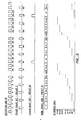
- Fig. 2 illustrates the generation of a dashed-line attribute format in which the image varies between five pixels of background level and five pixels of intensity M, for example.
- the background level intensity attribute is located at address N in attribute RAM 24, while the intensity level M is located at address N+1 in attribute RAM 24, for example.
- the central processing unit 28 supplies a starting address of N, a scaler count of 5, and a length count of 2.
- the first line of Fig. 2 illustrates the signal on vector generator control signal line 37, while the second line of the figure illustrates the addresses being supplied to refresh memory 12.
- Line 3 illustrates the output of scaler counter 42, while line 4 illustrates the output of address counter 36.
- Line 5 illustrates the output of length counter 46.
- line 6 illustrates the attribute which is output from attribute RAM 24.
- scaler counter 42 After the second set of five pulses has occurred, scaler counter 42 provides a second clock pulse. In response thereto, length counter 46 provides an output pulse which causes address counter 36 to reload the starting address from starting address register 38. Thus, the output of address counter 36 at this point is N. This pattern continues so long as pulses are provided on vector control line 37, or until central processing unit 28 provides the next instruction to the addressing circuitry 26.
- FIG. 3 an attribute format wherein the intensity level is permitted to increase every two pixels for a total of 128 pixels is illustrated.
- the first line of Fig. 3 depicts the signals on vector generator control line 37.
- the second line illustrates the scaler counter 42 output.
- the third and fourth lines illustrate the length counter output and the address counter output, respectively.
- the fifth line illustrates the graphical equivalent of the attribute information being supplied from attribute RAM 24.
- the scaler counter 42 is loaded with the number 2
- the length counter is loaded with length 64
- the starting address counter is loaded with address M.
- scaler counter 42 provides a pulse for every two pulses on the vector generator control line 37.
- address counter increments its output by 1, starting with starting address M.
- address counter 42 After the scaler counter 42 has output 64 pulses, corresponding to 128 pixels being addressed by vector generator 20, length counter 46 outputs a load pulse to address counter 36, thereby causing the original starting address M to be loaded into address counter 36.
- a stair step-like attribute is created by this format.
- parameter RAM 24 can be a 256 x 4 RAM comprising four 256 x 1 random access memories which are addressed in parallel.
- Commercially available parts such as industry number 10422, manufactured by Motorola, Inc. of Phoenix, Arizona are suitable for use in such an application.
- the counter functional blocks 46, 36 and 42 can be industry part number 10136, manufactured by Motorola, Inc. of Phoenix, Arizona.
- registers 48, 38 and 44 can be commercial part number 74LS374, manufactured by Signetics Corporation of Sunnyvale, CA.
- a storage means which stores a plurality of different attribute data at selected locations provides attribute data to a refresh memory associated with a visual display device, in conjunction with addresses supplied thereto by a vector address generator. Addressing for the storage means is supplied from an address generator.
- the method of the present invention comprises the steps of storing a plurality of different attributes at selected addresses in the storage means, providing an attribute format instruction to the addressing means, addressing the storage means in accordance with the attribute format instruction, wherein the addressing step includes the steps of starting the addressing at a specified starting address, incrementing the address whenever a predetermined number of pixel addresses has been supplied to the refresh memory by the vector address generator, wherein the predetermined number is supplied in the attribute format instruction, and restarting the addressing from the starting address when a predetermined number of increment counts has been supplied wherein the predetermined number is provided in the attribute format instruction.
Landscapes
- Engineering & Computer Science (AREA)
- Physics & Mathematics (AREA)
- Computer Hardware Design (AREA)
- General Physics & Mathematics (AREA)
- Theoretical Computer Science (AREA)
- Controls And Circuits For Display Device (AREA)
- Processing Or Creating Images (AREA)
- Digital Computer Display Output (AREA)
- Image Generation (AREA)
Claims (14)
Priority Applications (1)
| Application Number | Priority Date | Filing Date | Title |
|---|---|---|---|
| AT84902290T ATE57439T1 (de) | 1983-05-25 | 1984-05-23 | Verfahren und vorrichtung zum erzeugen von vektorattributen. |
Applications Claiming Priority (2)
| Application Number | Priority Date | Filing Date | Title |
|---|---|---|---|
| US49802583A | 1983-05-25 | 1983-05-25 | |
| US498025 | 1983-05-25 |
Publications (3)
| Publication Number | Publication Date |
|---|---|
| EP0146594A1 EP0146594A1 (de) | 1985-07-03 |
| EP0146594A4 EP0146594A4 (de) | 1987-07-23 |
| EP0146594B1 true EP0146594B1 (de) | 1990-10-10 |
Family
ID=23979314
Family Applications (1)
| Application Number | Title | Priority Date | Filing Date |
|---|---|---|---|
| EP19840902290 Expired EP0146594B1 (de) | 1983-05-25 | 1984-05-23 | Verfahren und vorrichtung zum erzeugen von vektorattributen |
Country Status (5)
| Country | Link |
|---|---|
| EP (1) | EP0146594B1 (de) |
| JP (1) | JPS60501575A (de) |
| AU (1) | AU2966984A (de) |
| DE (1) | DE3483390D1 (de) |
| WO (1) | WO1984004832A1 (de) |
Families Citing this family (3)
| Publication number | Priority date | Publication date | Assignee | Title |
|---|---|---|---|---|
| US4837563A (en) * | 1987-02-12 | 1989-06-06 | International Business Machine Corporation | Graphics display system function circuit |
| NL194254C (nl) * | 1992-02-18 | 2001-10-02 | Evert Hans Van De Waal Jr | Inrichting voor het converteren en/of integreren van beeldsignalen. |
| EP0676721A3 (de) * | 1994-04-06 | 1996-04-03 | Hewlett Packard Co | System zur Darstellung stilisierter Vektoren. |
Family Cites Families (7)
| Publication number | Priority date | Publication date | Assignee | Title |
|---|---|---|---|---|
| JPS5297632A (en) * | 1976-02-12 | 1977-08-16 | Hitachi Ltd | Display unit |
| US4225861A (en) * | 1978-12-18 | 1980-09-30 | International Business Machines Corporation | Method and means for texture display in raster scanned color graphic |
| JPS56111884A (en) * | 1980-02-08 | 1981-09-03 | Hitachi Ltd | Refreshing system for display picture |
| US4342991A (en) * | 1980-03-10 | 1982-08-03 | Multisonics, Inc. | Partial scrolling video generator |
| US4366476A (en) * | 1980-07-03 | 1982-12-28 | General Electric Company | Raster display generating system |
| JPS57501652A (de) * | 1980-10-27 | 1982-09-09 | ||
| US4368466A (en) * | 1980-11-20 | 1983-01-11 | International Business Machines Corporation | Display refresh memory with variable line start addressing |
-
1984
- 1984-05-23 EP EP19840902290 patent/EP0146594B1/de not_active Expired
- 1984-05-23 JP JP59502281A patent/JPS60501575A/ja active Pending
- 1984-05-23 DE DE8484902290T patent/DE3483390D1/de not_active Expired - Fee Related
- 1984-05-23 WO PCT/US1984/000787 patent/WO1984004832A1/en not_active Ceased
- 1984-05-23 AU AU29669/84A patent/AU2966984A/en not_active Abandoned
Also Published As
| Publication number | Publication date |
|---|---|
| JPS60501575A (ja) | 1985-09-19 |
| WO1984004832A1 (en) | 1984-12-06 |
| AU2966984A (en) | 1984-12-18 |
| EP0146594A1 (de) | 1985-07-03 |
| DE3483390D1 (de) | 1990-11-15 |
| EP0146594A4 (de) | 1987-07-23 |
Similar Documents
| Publication | Publication Date | Title |
|---|---|---|
| US4808986A (en) | Graphics display system with memory array access | |
| US4482979A (en) | Video computing system with automatically refreshed memory | |
| US4777485A (en) | Method and apparatus for DMA window display | |
| US5678037A (en) | Hardware graphics accelerator system and method therefor | |
| CA2130050C (en) | Method and apparatus for constructing a frame buffer with a fast copy means | |
| JPH0816836B2 (ja) | 情報処理方法 | |
| US4566000A (en) | Image display apparatus and method having virtual cursor | |
| EP0279225B1 (de) | Zähler mit veränderbarer Verschaltung zur Adressierung in graphischen Anzeigesystemen | |
| US4706074A (en) | Cursor circuit for a dual port memory | |
| US5670993A (en) | Display refresh system having reduced memory bandwidth | |
| EP0279227B1 (de) | Vektorgenerator für Raster-Bildschirmanzeige | |
| US4309700A (en) | Cathode ray tube controller | |
| US4119953A (en) | Timesharing programmable display system | |
| JPS5912176B2 (ja) | デイジタル・テレビジヨン・デイスプレイのためのカ−ソル回路 | |
| EP0312720A2 (de) | Graphik-Entwurfssystem mit Doppel-Pufferspeicher | |
| EP0146594B1 (de) | Verfahren und vorrichtung zum erzeugen von vektorattributen | |
| CA1200025A (en) | Graphic and textual image generator for a raster scan display | |
| JPH0646378B2 (ja) | コンピュータ表示装置 | |
| US6344856B1 (en) | Text optimization | |
| US4849748A (en) | Display control apparatus with improved attribute function | |
| US4646262A (en) | Feedback vector generator for storage of data at a selectable rate | |
| US5777631A (en) | Method and apparatus for displaying a video window in a computer graphics display | |
| US4511892A (en) | Variable refresh rate for stroke CRT displays | |
| US5239626A (en) | Display and drawing control system | |
| CN1167941A (zh) | 窗口化vga图象的设备和方法 |
Legal Events
| Date | Code | Title | Description |
|---|---|---|---|
| PUAI | Public reference made under article 153(3) epc to a published international application that has entered the european phase |
Free format text: ORIGINAL CODE: 0009012 |
|
| 17P | Request for examination filed |
Effective date: 19850122 |
|
| AK | Designated contracting states |
Designated state(s): AT BE CH DE FR GB LI LU NL SE |
|
| A4 | Supplementary search report drawn up and despatched |
Effective date: 19870723 |
|
| 17Q | First examination report despatched |
Effective date: 19880802 |
|
| GRAA | (expected) grant |
Free format text: ORIGINAL CODE: 0009210 |
|
| AK | Designated contracting states |
Kind code of ref document: B1 Designated state(s): AT BE CH DE FR GB LI LU NL SE |
|
| PG25 | Lapsed in a contracting state [announced via postgrant information from national office to epo] |
Ref country code: SE Effective date: 19901010 Ref country code: NL Effective date: 19901010 Ref country code: BE Effective date: 19901010 Ref country code: AT Effective date: 19901010 |
|
| REF | Corresponds to: |
Ref document number: 57439 Country of ref document: AT Date of ref document: 19901015 Kind code of ref document: T |
|
| REF | Corresponds to: |
Ref document number: 3483390 Country of ref document: DE Date of ref document: 19901115 |
|
| ET | Fr: translation filed | ||
| NLV1 | Nl: lapsed or annulled due to failure to fulfill the requirements of art. 29p and 29m of the patents act | ||
| PG25 | Lapsed in a contracting state [announced via postgrant information from national office to epo] |
Ref country code: LU Free format text: LAPSE BECAUSE OF NON-PAYMENT OF DUE FEES Effective date: 19910531 |
|
| PGFP | Annual fee paid to national office [announced via postgrant information from national office to epo] |
Ref country code: GB Payment date: 19910610 Year of fee payment: 8 |
|
| PGFP | Annual fee paid to national office [announced via postgrant information from national office to epo] |
Ref country code: FR Payment date: 19910619 Year of fee payment: 8 |
|
| PGFP | Annual fee paid to national office [announced via postgrant information from national office to epo] |
Ref country code: CH Payment date: 19910627 Year of fee payment: 8 |
|
| PGFP | Annual fee paid to national office [announced via postgrant information from national office to epo] |
Ref country code: DE Payment date: 19910628 Year of fee payment: 8 |
|
| PLBE | No opposition filed within time limit |
Free format text: ORIGINAL CODE: 0009261 |
|
| STAA | Information on the status of an ep patent application or granted ep patent |
Free format text: STATUS: NO OPPOSITION FILED WITHIN TIME LIMIT |
|
| 26N | No opposition filed | ||
| PG25 | Lapsed in a contracting state [announced via postgrant information from national office to epo] |
Ref country code: GB Effective date: 19920523 |
|
| PG25 | Lapsed in a contracting state [announced via postgrant information from national office to epo] |
Ref country code: LI Effective date: 19920531 Ref country code: CH Effective date: 19920531 |
|
| GBPC | Gb: european patent ceased through non-payment of renewal fee |
Effective date: 19920523 |
|
| PG25 | Lapsed in a contracting state [announced via postgrant information from national office to epo] |
Ref country code: FR Effective date: 19930129 |
|
| REG | Reference to a national code |
Ref country code: CH Ref legal event code: PL |
|
| PG25 | Lapsed in a contracting state [announced via postgrant information from national office to epo] |
Ref country code: DE Effective date: 19930202 |
|
| REG | Reference to a national code |
Ref country code: FR Ref legal event code: ST |