EP0146383B1 - Apparatus for forming electron beams - Google Patents
Apparatus for forming electron beams Download PDFInfo
- Publication number
- EP0146383B1 EP0146383B1 EP84308798A EP84308798A EP0146383B1 EP 0146383 B1 EP0146383 B1 EP 0146383B1 EP 84308798 A EP84308798 A EP 84308798A EP 84308798 A EP84308798 A EP 84308798A EP 0146383 B1 EP0146383 B1 EP 0146383B1
- Authority
- EP
- European Patent Office
- Prior art keywords
- cathode
- anode
- members
- hole
- grid
- Prior art date
- Legal status (The legal status is an assumption and is not a legal conclusion. Google has not performed a legal analysis and makes no representation as to the accuracy of the status listed.)
- Expired
Links
- 238000010894 electron beam technology Methods 0.000 title claims description 86
- OAICVXFJPJFONN-UHFFFAOYSA-N Phosphorus Chemical compound [P] OAICVXFJPJFONN-UHFFFAOYSA-N 0.000 claims description 53
- 239000007789 gas Substances 0.000 claims description 49
- 239000011521 glass Substances 0.000 claims description 34
- 229910000833 kovar Inorganic materials 0.000 claims description 17
- 239000011810 insulating material Substances 0.000 claims description 16
- 239000000463 material Substances 0.000 claims description 16
- 239000012777 electrically insulating material Substances 0.000 claims description 14
- 239000001307 helium Substances 0.000 claims description 13
- 229910052734 helium Inorganic materials 0.000 claims description 13
- SWQJXJOGLNCZEY-UHFFFAOYSA-N helium atom Chemical compound [He] SWQJXJOGLNCZEY-UHFFFAOYSA-N 0.000 claims description 13
- 230000015572 biosynthetic process Effects 0.000 claims description 10
- WFKWXMTUELFFGS-UHFFFAOYSA-N tungsten Chemical compound [W] WFKWXMTUELFFGS-UHFFFAOYSA-N 0.000 claims description 9
- 229910052721 tungsten Inorganic materials 0.000 claims description 9
- 239000010937 tungsten Substances 0.000 claims description 9
- 238000004891 communication Methods 0.000 claims description 6
- 239000004020 conductor Substances 0.000 claims description 6
- 239000011159 matrix material Substances 0.000 claims description 3
- 230000001419 dependent effect Effects 0.000 claims 1
- 229910052751 metal Inorganic materials 0.000 description 10
- 239000002184 metal Substances 0.000 description 10
- 208000028659 discharge Diseases 0.000 description 9
- XKRFYHLGVUSROY-UHFFFAOYSA-N Argon Chemical compound [Ar] XKRFYHLGVUSROY-UHFFFAOYSA-N 0.000 description 4
- YZCKVEUIGOORGS-OUBTZVSYSA-N Deuterium Chemical compound [2H] YZCKVEUIGOORGS-OUBTZVSYSA-N 0.000 description 4
- 229910052805 deuterium Inorganic materials 0.000 description 4
- 239000000758 substrate Substances 0.000 description 4
- 230000000694 effects Effects 0.000 description 3
- 230000005457 Black-body radiation Effects 0.000 description 2
- PXHVJJICTQNCMI-UHFFFAOYSA-N Nickel Chemical compound [Ni] PXHVJJICTQNCMI-UHFFFAOYSA-N 0.000 description 2
- 229910052786 argon Inorganic materials 0.000 description 2
- 229910052788 barium Inorganic materials 0.000 description 2
- DSAJWYNOEDNPEQ-UHFFFAOYSA-N barium atom Chemical compound [Ba] DSAJWYNOEDNPEQ-UHFFFAOYSA-N 0.000 description 2
- 239000010406 cathode material Substances 0.000 description 2
- 239000000919 ceramic Substances 0.000 description 2
- 238000005553 drilling Methods 0.000 description 2
- 230000005284 excitation Effects 0.000 description 2
- 238000004519 manufacturing process Methods 0.000 description 2
- 239000010453 quartz Substances 0.000 description 2
- 238000007363 ring formation reaction Methods 0.000 description 2
- VYPSYNLAJGMNEJ-UHFFFAOYSA-N silicon dioxide Inorganic materials O=[Si]=O VYPSYNLAJGMNEJ-UHFFFAOYSA-N 0.000 description 2
- RYGMFSIKBFXOCR-UHFFFAOYSA-N Copper Chemical compound [Cu] RYGMFSIKBFXOCR-UHFFFAOYSA-N 0.000 description 1
- ZOKXTWBITQBERF-UHFFFAOYSA-N Molybdenum Chemical compound [Mo] ZOKXTWBITQBERF-UHFFFAOYSA-N 0.000 description 1
- RTAQQCXQSZGOHL-UHFFFAOYSA-N Titanium Chemical compound [Ti] RTAQQCXQSZGOHL-UHFFFAOYSA-N 0.000 description 1
- 229910045601 alloy Inorganic materials 0.000 description 1
- 239000000956 alloy Substances 0.000 description 1
- 230000004075 alteration Effects 0.000 description 1
- 239000004411 aluminium Substances 0.000 description 1
- 229910052782 aluminium Inorganic materials 0.000 description 1
- XAGFODPZIPBFFR-UHFFFAOYSA-N aluminium Chemical compound [Al] XAGFODPZIPBFFR-UHFFFAOYSA-N 0.000 description 1
- 238000002048 anodisation reaction Methods 0.000 description 1
- 230000004323 axial length Effects 0.000 description 1
- 229910052802 copper Inorganic materials 0.000 description 1
- 239000010949 copper Substances 0.000 description 1
- 238000010586 diagram Methods 0.000 description 1
- 238000010438 heat treatment Methods 0.000 description 1
- 238000003754 machining Methods 0.000 description 1
- 150000002739 metals Chemical class 0.000 description 1
- 238000000034 method Methods 0.000 description 1
- 239000000203 mixture Substances 0.000 description 1
- 238000012986 modification Methods 0.000 description 1
- 230000004048 modification Effects 0.000 description 1
- 229910052750 molybdenum Inorganic materials 0.000 description 1
- 239000011733 molybdenum Substances 0.000 description 1
- 229910052754 neon Inorganic materials 0.000 description 1
- GKAOGPIIYCISHV-UHFFFAOYSA-N neon atom Chemical compound [Ne] GKAOGPIIYCISHV-UHFFFAOYSA-N 0.000 description 1
- 229910052759 nickel Inorganic materials 0.000 description 1
- 230000000149 penetrating effect Effects 0.000 description 1
- 239000003870 refractory metal Substances 0.000 description 1
- 238000004611 spectroscopical analysis Methods 0.000 description 1
- 229910052715 tantalum Inorganic materials 0.000 description 1
- GUVRBAGPIYLISA-UHFFFAOYSA-N tantalum atom Chemical compound [Ta] GUVRBAGPIYLISA-UHFFFAOYSA-N 0.000 description 1
- 239000010936 titanium Substances 0.000 description 1
- 229910052719 titanium Inorganic materials 0.000 description 1
Images





Classifications
-
- H—ELECTRICITY
- H01—ELECTRIC ELEMENTS
- H01J—ELECTRIC DISCHARGE TUBES OR DISCHARGE LAMPS
- H01J17/00—Gas-filled discharge tubes with solid cathode
- H01J17/02—Details
- H01J17/04—Electrodes; Screens
- H01J17/06—Cathodes
- H01J17/066—Cold cathodes
Definitions
- This invention relates to apparatus for forming electron beams, and to apparatus requiring the formation of electron beams, such as, for example, display devices and thyratrons.
- US-A-4 196 938 describes a glow discharge chamber electrode which includes a metal body covered in dielectric except for an emitting zone.
- GB-A-1 145 013 is concerned with a glow discharge device in which an electrode arrangement is used to focus and direct electrons produced by a glow discharge.
- GB-A-603 088 discloses a cold cathode device in which cratering of the cathode is reduced by the inclusion of a bore in the cathode surface.
- the present invention seeks to provide improved apparatus for forming an electron beams.
- apparatus for forming an electron beam comprising, within an envelope, an anode member; a cathode member of electrically conductive material; means for applying a voltage between the anode member and cathode member; and a gas filling, and wherein, except for part of a front surface of said cathode member, substantially the whole of the surface of said cathode member which would otherwise be exposed to the gas filling within said envelope is covered with an electrically insulating material, the gas pressure, voltage and electrode arrangement being such that, upon the application of the voltage between said anode member and said cathode member,a discharge is produced which is characterized by the formation of an electron beam extensive in a direction away from said part of said front surface.
- said part is a hole in the said front surface, the whole arrangement being such that upon the application of a suitably high voltage between said anode member and said cathode member a highly directional electron beam is formed extensive in a direction away from said hole.
- the anode member may be located in front of the front surface of the cathode member.
- a control grid electrode is included through which operation the electron beam passes, enabling the intensity or energy of the electron beam to be modulated.
- the apparatus includes a plurality of elongate cathode members arranged in a grid formation, and a plurality of elongate anode members arranged in a grid formation with said grid of anode members superimposed over said grid of cathode members, but spaced therefrom, with said anode members in crossing relationship with said cathode members to form a matrix, each of said cathode members having a series of holes entering into its surface facing said grid of anode members and each of said anode members having a series of holes passing therethrough, with each hole in an anode member aligned with a hole in a different one of the cathode members, and all surfaces of said cathode members, except for surfaces within said holes in said cathode members, which would otherwise be exposed to said gas filling are isolated therefrom by electrically insulating material, and the whole arrangement being such that by applying a high potential between one of said anode members and one of said cathode members an electron beam is formed at the crossing
- an electron beam may be created which, by varying the selection of anode and cathode members addressed may be caused to be animated.
- insulating material is interposed between said grid of cathode members and said grid of anode members, which insulating material has passages therethrough aligned with said holes in said cathode and anode members whereby to permit communication between one cathode hole and the appropriate anode hole but impede communication between that cathode hole and any other anode hole.
- said last-mentioned interposed insulating material is provided in the form of a slab having holes extending between its major surfaces and forming the said passages.
- a control grid electrode may be located on the side of the grid of anode members other than that on which the grid of cathode members is located, or alternatively it may be located between the grid of cathode members and the grid of anode members, and where insulating material is interposed between the cathode and anode grids the control grid electrode may be embedded in the interposed insulating material.
- the anode member may be to one side of the axis of the electron beam formed in operation, such that said beam passes by said anode. It has been found by the inventors that the electron beam may be formed along the axis of the hole even though the anode member is displaced to the side of its path.
- the anode member is located behind said front surface of the cathode member, and again in this configuration the electron beam may be formed along the axis of the hole, rather than along the shortest path between the anode and cathode members.
- the anode member is co-axial with the cathode member.
- a grid is included through which in operation the electron beam passes, enabling it to be modulated in intensity or energy, although of course, this may be achieved by varying the high voltage between the anode and cathode members.
- a plurality of elongate anode members each having apertures therein; and a plurality of stemmed cathode members, each having a hole in the front surface thereof and arranged such that its stem extends through one of said apertures, such that each anode member is located behind the front surfaces of cathode members whose stems pass through apertures in said anode member, whereby by applying a high potential between an anode member and one of the cathode members extending through an aperture therein an electron beam is formed extensive in a direction away from the hole in said one of the cathode members.
- an electron beam may be formed in a desired location, or number of such beams formed simultaneously if cathode members may be individually addressed.
- a cathode member extending through an aperture in one anode member is electrically connected to another cathode member extending through an aperture in another anode member and also preferably a connector connecting two cathode members is spaced from the anode members by electrically insulating material.
- a phosphor layer is included and is aranged so that when an electron beam is formed it impinges upon a spot upon said layer whereby to excite the same and preferably said envelope has a portion formed as a faceplate on the interior of which said phosphor layer is provided.
- a video signal reproducing apparatus includes apparatus as described above.
- a cathode ray tube apparatus comprises a plurality of elongate cathode members arranged in a grid formation, a plurality of elongate anode members arranged in a grid formation with said grid of anode members superimposed over said grid of cathode members, but space therefrom, with said anode members in crossing relationship with said cathode members to form a matrix, each of said cathode members having a plurality of holes entering into its surface facing said grid of anode members and each of said anode members having a plurality of holes passing therethrough, with each hole in an anode member aligned with a hole in a different one of the cathode members and, superimposed over said grid of anode members on the side thereof remote from said grid of cathode members, a phosphor screen, the two grids being enclosed within an envelope having a gas filling from which all surfaces of said cathode members, except for surfaces within said holes in said catho
- the longitudinal axis of said hole may be oblique to the normal of said front surface, and the electron beam is formed normal to said front surface of said hole.
- the inventors discovered that, when the hole is arranged with its longitudinal axis inclined to the normal of the front surface, an electron beam is not formed parallel to the aforesaid axis as might be expected but is in fact, surprisingly, formed in a direction normal to the front surface.
- the term "normal” it should be taken to include “substantially normal”. Apparatus utilising this principle may be useful where, for example, space is restricted and it would not be possible to employ a device in which the hole is arranged normal to the surface of the cathode. Also manufacture of the device is facilitated since only the direction of the front surface need be accurately machined.
- Such apparatus may include a plurality of holes in said front surface, at least one of said holes having its longitudinal axis oblique to the normal of said front surface at that hole, such that upon the application of said suitably high voltage electron beams are formed extensive normal to said front surface at and in a direction away from respective holes. Since the configuration of the front surface was found by the inventors to determine the direction of electron beams produced, a desired pattern of electron beams or concentration of electron beams may be achieved without costly machining. For example, if a plurality of beams which are mutually parallel are required the holes need not be drilled in precise relationship to each other, as might have been thought, as only the front surface need be made flat. Of course the front surface can be curved if more complex patterns are required, and because of leniency in the disposition of the holes the cathode member may be more conveniently shaped for a desired application.
- the cathode member of electrically conductive material has a front surface which is curved; and, except for a plurality of discrete parts of the said front surface, at least substantially the whole of the surface of said cathode member which would otherwise be exposed to the gas filling within said envelope is covered with an electrically insulating material, the whole arrangement being such that upon the application of a suitably high voltage between said anode member and said cathode member electron beams are formed extensive normal to said front surface at and in a direction away from respective parts.
- the front surface is curved such that they are focussed or concentrated at a point or small region. This is a particularly useful configuration providing apparatus suitable for inclusion in an electron beam welder, or as a point source of soft X-rays or incandescent black body radiation.
- a layer of phosphor material on a viewable screen arranged such that upon the application of said suitably high voltage the electron beam impinges upon said phosphor layer and so excites the same.
- a display apparatus comprises, within an envelope, a layer of phosphor material on a viewable screen; remote from said phosphor layer, a metallic cathode member having a hole formed in a front surface thereof; between said cathode member and said phosphor layer, an apertured anode electrode; and a gas filling, and wherein, except within said hole, at least substantially the whole of the surface of said cathode member which would otherwise be exposed to the gas filling within said envelope is covered with an electrically insulating material, the whole arrangement being such that upon the application of a suitably high voltage between said anode member and said cathode member an electron beam is formed extensive in the space between the mouth of the hole in said cathode member and said anode member, and is arranged to penetrate through an aperture in said anode member to impinge upon said phosphor layer and so excite the same.
- said envelope has a portion formed as a faceplate upon the inner surface of which said phosphor layer is provided.
- the apparatus may include a modulating grid provided to affect the strength or intensity of the electron beam impinging upon said phosphor layer.
- Said modulating grid may be a perforated grid or gauze provided either between said anode member and said phosphor layer or between said anode member and said cathode member.
- said modulating grid comprises a ring grid provided within the mouth of said hole in said cathode member.
- an electrical connection for said grid is taken out, in insulated fashion through said cathode member in a direction away from said anode member, i.e. through the base of said cathode member.
- said cathode member is provided for by means of an electrical connector connected to the base of said cathode member, said last mentioned connector is preferably in the form of a hollow cylinder with an electrical connector for said grid passing, in insulated fashion, therethrough.
- a single hole in said cathode member with a corresponding single aperture in said anode member may be provided in said cathode member with a corresponding plurality of holes in said anode member.
- a plurality of holes and apertures may be in ring formation, with or without a centrally disposed hole and aperture.
- thyratron apparatus comprises, within an envelope, an anode member; a cathode member of electrically conductive material and having a hole in a front surface thereof; and a gas filling, and wherein, except within said hole, at least substantially the whole of the surface of said cathode member which would otherwise be exposed to the gas filling within said envelope is covered with an electrically insulating material, the whole arrangement being such that upon the application of a suitably high voltage between said anode member and said cathode member an electron beam is formed extensive in a direction away from said hole.
- said cathode member has a plurality of holes in the front surface thereof, such that upon application of a suitably high voltage electron beams are formed extensive in a direction away from respective holes, and it is preferred that said front surface is curved, such that some focussing of the electron beams to a point may be obtained. Also it is preferred, where the front surface is curved, that at least one of said holes has its longitudinal axis oblique to the normal of said front surface at that hole.
- the cathode member may form the cathode of a thyratron, or advantageously thermionic material may be included and arranged such that when an electron beam or beams are formed they heat the same. This heating may be direct or indirect. For example, a substrate carrying the thermionic material may be exposed to the electron beam or beams and heat transmitted to the thermionic material by conduction.
- the electron beam when it is formed, it may be arranged to ionize the gas filling in a localised region, and so improve operating characteristics of a thyratron, and advantageously the longitudinal axis of the hole is oblique to the nornmal of said front surface at the hole, enabling the cathode member to be accommodated in a restricted space.
- more than one such cathode member may be employed.
- the front surface may be shaped to focus said electron beam.
- the electron beam may be focussed.
- Each point of the surface around the mouth of the hole and at its edge may be thought of as directing components of the electron beam normal to the surface at respective points.
- a desired degree of focussing may be obtained.
- the electron beam may be focussed to a point or it could be focussed merely enough to aid in further collimation of the electron beam.
- each hole in a cathode member is blind, and preferably of circular cross-section.
- said insulating material insulating surfaces of said cathode member, or plurality of cathode members, from said gas filling is glass, but where said cathode member, or members, is of an anodisable metal, such as aluminium or titanium, the insulating material may be anodisation.
- cathode and anode members are of Kovar but other metals or alloys may be used, such as aluminiumm copper or tungsten, or of molybdenum, tantalum or other refractory metals for high current use.
- said envelope is of glass or quartz.
- each hole is entirely free of a covering of electrically insulating material.
- a number of gases, or mixture of gases, may be used for said gas filling including helium and/or argon and/or deuterium and/or neon.
- the hole size and voltages applied are related to the type of gas employed. Typically, hole sizes for argon are 0.2 to 0.1 of the size of those for helium, giving the possibility of more compact devices.
- said gas filling is at a pressure of between 0.5 and 2.5 mB.
- the higher voltage utilised to address the anode and cathode members is from 1 to 5 kV and preferably between 1 and 2.5 kV.
- a device comprises a quartz envelope of which only one portion 1 is shown.
- the envelope portion 1 is provided as a faceplate having on its interior a layer 2 of phosphor material similar to that used in conventional cathode ray display tubes.
- a transparent metal layer (not shown but somewhat akin to the transaparent metal layer forming part of the screen of a conventional cathode ray tube) between the layer 2 and the faceplate.
- the faceplate formed by the portion 1 of the envelope of the device is transparent.
- a cathode member 3 which comprises a block 4 of Kovar having a blind hole 5 formed therein, in this case by drilling coaxially with the axis of cylindrical symmetry 6 of the device.
- the open mouth of the hole 5 faces the phosphor layer 2.
- a connecting pin 7 is inserted in the base of the block 4, adjacent the blind end of the hole 5, so as to enable electrical connection to be made to the Kovar block 4.
- the insulating material 8 is glass.
- anode electrode 9 which has a circular hole 10 passing therethrough. Circular hole 10 is coaxially aligned with the blind hole 5 within the Kovar block 4.
- the cathode 3 is devoid of a heater as such, or any electron emissive cathode material, such as barium.
- the envelope of the tube is filled with helium at a pressure of between 0.2 and 10 mB.
- the dimensions of the cathode and anode holes 5 and 10 and the spacing of the anode 9 to the cathode 3 is suitably chosen, a type of electrical discharge will be established between the anode 9 and the cathode 3 which results in the formation of an electron beam along the axis 6 of the coaxially aligned anode and cathode holes when a potential difference in the range of from several hundred volts to several thousand volts is established between the anode 9 and the block 4 of cathode 3.
- the electron beam acquires energy approximately equal to the anode to cathode potential difference and so extends into the region beyond the anode hole 10 to impinge, finally, upon the phosphor layer 2 thus exciting it.
- the device With a gas filling of helium at a pressure of 2 mB and a potential difference between anode 9 and cathode 3 of approximately 1.5 kV, the device was found to operate with a spacing between the plane of the anode 9 and the surface of the phosphor layer 2 of up to a few centimetres, and a spacing between the anode 9 and the cathode 3 of at least 3 mm. With the above-mentioned potential difference of 1.5 kV the current drawn from the cathode, was of the order of 15 mA.
- modulation of the intensity or energy of the electron beam arriving at the surface of the phosphor layer 2 may be achieved by varying a potential applied to the grid 11.
- varying the potential between the anode 9 and the cathode 3 will produce or enhance a modulation effect but, of course, it is much less convenient to apply modulation at high potential.
- a mesh grid such as 11 in Figure 1 is not provided betwen the anode 9 and the phosphor layer 2.
- a ring grid 11' is provided within the mouth of the blind hole 5 in the Kovar block 4. Electrical connection is made to the ring grid 11' by means of a connector passing out through the base of the Kovar block 4.
- the contact here referenced 7' is cylindrical with the connecting lead for the grid 11' passing coaxially therethrough in insulated fashion.
- insulating material would be provided to support the connecting lead for the grid 11 within the cylindrical connector 7'.
- the graph of Figure 4 shows the relationship between beam current I and cathode fall voltage V (i.e. the voltage applied between anode and cathode) for different gas filling pressures, for a device as described above having cathode and anode holes of 5 mm in diameter.
- a plurality of blind holes may be provided in the Kovar block 4 with each cathode hole being coaxially aligned with a corresponding hole passing through the anode member 9.
- the holes will be arranged in a ring formation, with or without cathode and anode holes on-centre.
- THe effect achieved using a plurality of cathode and anode holes in a simple device as illustrated in Figures 1 to 3, is that the areas of excitation thus created in the phosphor layer 2 tend to merge to produce a larger illuminated spot (or other prescribed pattern as determined by the pattern of holes on the faceplate 1) than would otherwise be the case.
- the graph of Figure 5 shows parameters for this last-mentioned case corresponding to those shown in the graph of Figure 4 for this embodiment shown in Figure 1.
- One application for a device as described above is in large area displays such as those sometimes found in public places in order to impart information, e.g. in airport terminals or sports areas.
- devices such as those described above in rows and columns and addressing individual devices appropriately, letters and words - and even graphics - may be produced.
- another device in accordance with the invention includes a glass envelope 12 which is of generally circular cross-section and has a transversely extending side-arm 13 about mid-way along its length.
- An anode member 14 extends through the end wall of the side-arm 13 and into the main part of the volume enclosed by the envelope 12.
- a cathode member 15 passes through an end wall of the envelope 12. It has a stem portion 15A and an enlarged end 15B with a blind hole 16 of circular cross-section in its front surface. All of the surfaces of the cathode member 15 contained within the envelope 12, except for the side wall and base surfaces of the hole 16, are coated with a layer of glass 17.
- the envelope 12 contains helium at a pressure of 2 mB.
- a potential difference of about 1 kV is applied across the anode and cathode members 14 and 15 and an electron beam is formed along the axis A-A of the hole 16.
- the envelope 12 has a length of about 7 cm and a diameter of about 3.5 cm.
- the anode and cathode members 14 and 15 are separated by approximately 1 cm in the axial direction and 0.5 cm in the transverse direction.
- the diameter of the hole 16 is 5 mm, with a depth (i.e. axial length) of 3 mm.
- a display device comprises a plurality of elongate cathode members C1 to C4 arranged parallel to one another to form a grid.
- Each cathode member as shown in Figure 10, comprises a bar of Kovar having at regular intervals along its length blind holes 18. The holes 18 extend into the same planar surface of the cathode member.
- Each cathode member is provided with an electrical connector (not shown) by means of which it may be individually addressed.
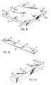
- anode memebers A1 to A5 each of which consists of a bar of Kovar having a series of holes 19 passing therethrough from one planar face to its opposite planar face as illustrated in Figure 9.
- the pitch of the holes 19 in an anode member corresponds to the spacing between the cathode members in the cathode grid and the spacing of the anode members in the anode grid corresponds to the pitch of the cathode holes 18 in a cathode member so that each cathode hole 18 is aligned with an anode hole 19 at the crossing point of the anode and cathode conductors in which those particular holes appear.
- a slab 20 of glass Sandwiched between the grid of cathode members and the grid of anode members is a slab 20 of glass which has rows and columns of holes 21 therein extending from one major planar face to its opposite major planar face, as illustrated in Figure 8.
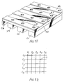
- the rows and columns of holes are spaced such that when the slab is sandwiched between the grid of cathode members and the grid of anode members, as shown in Figure 11, each aligned cathode and anode hole at the crossing point of an anode and cathode member is also aligned with a hole in the slab of insulating material 20.
- the holes 21 in the insulating slab 20 permit communication between appropriate ones of the cathode and anode holes 18 and 19 but impede communication between each cathode hole and other than the anode holes with which it is directly aligned. Thus the tendency for so-called "long path" discharges to take place is reduced.
- a phosphor screen comprising of a layer of phosphor material 22 on the inside of part of an enclosing envelope which is formed as a faceplate 23.
- a transparent layer of conductive material (somewhat akin to the transparent metal layer of the phosphor screen of a conventional cathode ray tube device) between the phosphor layer 22 and the faceplate 23.
- the envelope in this case is of glass and encloses the anode and cathode members together, of course, with the interposed slab of insulating material 20.
- the envelope has a gas filling of helium and, as illustrated only in Figure 7, each cathode member C is entirely covered with an electrically isolating layer 24 of glass, except within the holes 18.
- each cathode member C is entirely covered with an electrically isolating layer 24 of glass, except within the holes 18.
- all surfaces of the cathode members which would otherwise be exposed to the helium gas filling are isolated therefrom.
- all surfaces at cathode potential are so isolated from the gas filling.
- the wall and base surfaces of the holes 18 are entirely free from glass.
- the cathode and anode holes 18 and 21 are of circular cross-section with a diameter of 5 mm.
- the helium gas filling is at a pressure of 2 mB.
- the distance separating the grid of cathode members from the grid of anode members i.e. the thickness of the slab 20
- the distance separating the grid of anode members from the phosphor layer 22 is in the region of 0.5 to 2 cm.
- grid 25 shown in Figure 7 is located between the grid of anode members A and the phosphor layer 22.
- the purpose of this grid is to modulate the intensity or energy of the electron beams arriving at the phosphor.
- the overall intensity or energy of the electrons beams may be modulated or adjusted by appropriate alterations to the anode to cathode discharge current as determined by the voltage applied between the cathode and anode members.
- a grid 26 is embedded in the slab 20, as shown in Figures 13 and 14, and may comprise a gauze or as metal plate having holes which correspond to the anode and cathode holes, as illustrated in Figure 15.
- cathode heaters are employed in the device illustrated, the cathodes being cold cathodes, and no cathode material such as barium is employed.
- another embodiment of the invention includes a cathode member 27 of Kovar having a hole 28 of about 5 mm diameter in its front surface and being enclosed in a glass envelope 29 which also contains helium gas at a pressure of about 2 mB and has a layer of phosphor on its inner surface to form a screen 30.
- the surfaces of the cathode member 27, except the side wall and base of the hole 28, are covered in a glass layer 31, which electrically insulates the cathode member 27 from the helium gas filling. Electrical connection to the cathode member 27 is made via a pin 32 which is sheathed with a layer 33 of glass.
- An anode member 34 is located between the front surface of the cathode member 27 and the phosphor screen 30, being about 2 cm from the cathode member 27, and 2 cm from the screen 30.
- the anode member 34 is also offset from the axis X-X of the hole 28, being about 2 cm to the right as shown.
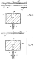
- the intensity of the spot may be varied by modulating the voltage applied to a grid electrode 35, shown in this embodiment to be positioned between the screen 30 and the anode member 34, although it could be located between the anode and cathode members 34 and 27.
- a cathode member 36 of Kovar has a hole 37 in its front surface and is coated with an electrically insulating layer of glass 38.
- the cathode member 36 is contained within a glass envelope 39 having on its inner surface a layer of phosphor which acts as a screen 40, and enclosing helium gas at 2 mB pressure.
- the cathode member 36 is electrically connected via a pin 41, which is also coated in glass 42, forming a stem.
- a Kovar anode member 43 is located behind the front surface of the cathode member 36 and is positioned co-axially with it about the pin 41.
- a modulating grid may also be included, and/or modulation may be carried out by varying the potential difference applied.
- the hole 37 has a diameter of about 5 mm and the front surface of the cathode member 36 may be between a few millimetres and a few centimetres from the screen 40.
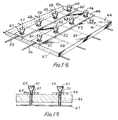
- a plurality of Kovar strips are arranged parallel to each other on a glass slab 46.
- Each of the strips has a plurality of apertures through it, only four of which, 47, 48, 49 and 50; 51, 52, 53 and 54 are shown for each strip.
- Each strip forms an anode member, electrical signals being applied to them via rods 55 and 56.
- Cathode members 57 to 64 are of Kovar and have stems extending through the apertures in the strips 44 and 45, there being one cathode member to each aperture, and passing through the glass slab 46.
- the surfaces of each cathode member, including the connecting pin comprising its stem, are coated in glass layers 65 and 66 except for the side wall and base of the single hole in each ones front surface.
- the ends of the cathode members 57 to 64 on the side of the glass slab 46 other than the anode strips 44 and 45 are connected via rods 67, 68, 69 and 70, such that one cathode member associated with one strip is electrically connected to a cathode member associated with each of the other strips, giving a crossing relationship between the cathode and anode members.
- rods 67, 68, 69 and 70 such that one cathode member associated with one strip is electrically connected to a cathode member associated with each of the other strips, giving a crossing relationship between the cathode and anode members.
- a display By placing the structure within an envelope filled with helium at 2 mB pressure, and having a phosphor screen on its inner surface, a display may be produced.
- the front surfaces of the cathode members 57 to 64 may be as litle as 5 mm from the surface of the screen, and a potential difference between the anode and cathode members of 1.5 kV would be required.
- a thorated tungsten cathode member 71 has a stem 72 via which electrical connection is made, and is covered with a layer 73 of electrically insulating glass which also extends to the stem 72.
- An anode member 74 surrounds and is coaxial with the stem 72.
- the cathode member 71 has a front surface 75 in which is formed a blind hole 76 of circular cross-section, being 5 mm deep and having a diameter of about 1.5 mm, and having surfaces which are free of the layer 73 of glass.
- the front surface 73 is inclined with respect to the hole 76 such that the longitudinal axis of the hole 76, shown as broken line 77, is oblique to the normal 78 of the front surface 75 at that point, the angle between them being about 3O o .
- the cathode and anode arrangement is enclosed within a glass envelope which also contains a gas filling of deuterium at about 2 mB pressure.
- a thorated tungsten cathode member 80 is connected to stem 81 and is contained within an envelope (not shown) together with a deuterium gas filling at about 2 mB pressure and an anode member 82, which is coaxial with and surrounds the stem 81.
- the cathode member 80 and stem 81 are coated with a layer 83 of glass which electrically insulates them from the deuterium gas filling.
- a plurality of holes 84 are formed in a front surface 85 of the cathode member 80, each of them being of circular cross-section with a diameter of about 1.5 mm and a depth of 5 mm and having surfaces which are free of the layer 83 of glass.
- the front surface 85 is curved, for example, it may be parabolically or spherically shaped, rather than the flat surface 75 shown in Figure 20.
- holes 84 are illustrated as being disposed mutually parallel, they could be arranged in some other way, since their attitude does not affect the directions of the electrons beams which are formed during operation.
- Apparatus according to the invention in which the surface is curved to produce such focussing might find application in an electron beam welder, for example, in which case the piece being welded may also be for example contained within the envelope. It might also find application in the production of a point source of soft X-rays, having a wavelength of about 6.1O -1O m, for use in spectroscopy for example, or to generate a point source of incandescent black body radiation.
- a thyratron in accordance with the invention includes a glass envelope 87, containing a gas filling, an anode 88, a screen grid 89 and control grids 9O and 91, such as might be found in a conventional thyratron.
- the cathode instead of the conventionally provided heated cathode, the cathode comprises a cathode member 92 of tungsten having a plurality of holes 93 in itsfront surface, facing the anode 88.
- the surface of the cathode member 92 is entirely covered with a glass layer 94 except for the walls and bases of the holes 93.
- a suitably high voltage is applied between the anode 88 and the cathode member 92 such that an electron beam is formed extensive in a direction away from each hole.
- the gas filling becomes ionized and a conduction path is established between the anode 88 and cathode member 92.
- another thyratron in accordance with the invention includes a glass envelope 95 containing a gas filling, an anode 96, a screen grid 97 and control grids 98 and 99. It also includes a conventional heated cathode, comprising a hollow cylinder 1OO of thermionic material and a heater filament 101.
- Two cathode members 102 and 103 are located within the glass envelope 95. Each has a hole 104 and 105 in its front surface and is coated with a glass layer 106 and 107. The longitudinal axes of the holes 104 and 105 are oblique to the front surfaces of the cathode members 102 and 103.
- the cathode members 102 and 103 also have stem portions 108 and 109 which are surrounded by coaxial anode members 110 and 111 respectively.
- the thermionic material 100 is heated by the heater filament 101 causing electrons to be emitted from its surface.
- the emitted electrons ionize that part of the gas filling between the controls grids 98 and 99 and the cathode to establish a primary discharge.
- a positive voltage pulse is applied to the control grids 98 and 99, allowing the discharge to penetrate through them to initiate the main discharge, and thus to render the thyratron conducting.
- a voltage may be applied between the cathode members 102 and 103 and the cathode members 110 and 111 respectiovely, such that electrons beams are formed extensive of the holes 104 and 105 and normal to the front surfaces of the cathode members 102 and 103, their path being shown by broken lines 112 and 113.
- These beams may be formed simultaneously with, or shortly before or after, the application of the voltage pulse to the controlgrids 98 and 99.
- the beams are arranged to pass through apertures in the control grids 98 and 99 and penetrate into the volume beyond them, to ionize the gas filling.
- the cathode members could be located elsewhere within the envelope 95 if it is desired to promote ionization in other regions of the thyratron, and of course only one, or more than two cathode members could be used.
- another thyratron includes a glass envelope 114, gas filling, an anode 115, a screen grid 116 and control grids 117 and 118.
- the thyratron includes a thermionic cathode 119 having thermionic material 12O carried by a substrate 121 of high thermal conductivity which may be nickel, for example.
- a cathode member 122 of tungsten is positioned on the substrate side of the cathode 12O.
- the cathode member 122 has a plurality of holes 123 in its front surface which is concave.
- the surface of the cathode member 122, except for the walls and bases of the holes 123, are covered with a layer 124 of glass.
- An anode member 125 surrounds the cathode member 122.
- a voltage is applied between the anode member 125 and the cathode member 122 such that a beam of electrons is formed extensive of each hole.
- the curved surface of the block 122 gives a focussing effect, and the electrons are directed to impinge on the substrate 121, their kinetic energy being converted into heat. Heat is conducted to the thermionic material 12O causing electrons to be emitted to produce ionization of the gas filling.
- a cathode member is formed by inserting a tungsten cylindrical rod 126 into a hollow tube 127 of an electrically insulating material, such as a ceramic or galss.
- Figure 26 illustrates another cathode member in which a tungsten rod 128 is inserted into a hollow metal tube 129, which may also be of tungsten, and a ceramic tube 13O is fitted over the metal tube 129. Any metal surfaces which would be exposed in use to a gas filling may then be covered with an insulating layer.
- cathode members of this type no drilling is required, as it is with those previously described.
- a device in accordance with the invention comprises within an envelope (not shown) which also contains a gas filling, a cylindrical cathode member 131 having a stem portion 132 via which electrical connection is made to the cathode member 131.
- the cathode member 131 has a front surface 132 of circular transverse cross-section which is of a 'dished' or frusto-conical configuration, the front surface being inclined such that the length of the cathode member 131 along its axis Z-Z increases from its centre to its circumference. Other surface configuration may of course be employed if desired.
- a hole 133 is located in the centre of the front surface 132 and is coaxial with axis Z-Z of the cathode member 131.
- the surfaces of the cathode member 131 and the stem portion 132 are covered with a layer 134 of electrically insulating glass,and an anode member 135 surrounds and is coaxial with the stem portion 132.
- the front surface is flat then a beam is produced which, although it is highly collimated, tends to diverge to some extent because of, for example, scattering processes. By using a front surface having a small degree of dishing, this tendency may be counteracted.
Landscapes
- Cathode-Ray Tubes And Fluorescent Screens For Display (AREA)
Description
- This invention relates to apparatus for forming electron beams, and to apparatus requiring the formation of electron beams, such as, for example, display devices and thyratrons.
- US-A-4 196 938 describes a glow discharge chamber electrode which includes a metal body covered in dielectric except for an emitting zone.
- GB-A-1 145 013 is concerned with a glow discharge device in which an electrode arrangement is used to focus and direct electrons produced by a glow discharge.
- GB-A-603 088 discloses a cold cathode device in which cratering of the cathode is reduced by the inclusion of a bore in the cathode surface.
- The present invention seeks to provide improved apparatus for forming an electron beams.
- According to the invention there is provided apparatus for forming an electron beam comprising, within an envelope, an anode member; a cathode member of electrically conductive material; means for applying a voltage between the anode member and cathode member; and a gas filling, and wherein, except for part of a front surface of said cathode member, substantially the whole of the surface of said cathode member which would otherwise be exposed to the gas filling within said envelope is covered with an electrically insulating material, the gas pressure, voltage and electrode arrangement being such that, upon the application of the voltage between said anode member and said cathode member,a discharge is produced which is characterized by the formation of an electron beam extensive in a direction away from said part of said front surface.
- Preferably, said part is a hole in the said front surface, the whole arrangement being such that upon the application of a suitably high voltage between said anode member and said cathode member a highly directional electron beam is formed extensive in a direction away from said hole.
- The anode member may be located in front of the front surface of the cathode member.
- Preferably a control grid electrode is included through which operation the electron beam passes, enabling the intensity or energy of the electron beam to be modulated.
- Preferably the apparatus includes a plurality of elongate cathode members arranged in a grid formation, and a plurality of elongate anode members arranged in a grid formation with said grid of anode members superimposed over said grid of cathode members, but spaced therefrom, with said anode members in crossing relationship with said cathode members to form a matrix, each of said cathode members having a series of holes entering into its surface facing said grid of anode members and each of said anode members having a series of holes passing therethrough, with each hole in an anode member aligned with a hole in a different one of the cathode members, and all surfaces of said cathode members, except for surfaces within said holes in said cathode members, which would otherwise be exposed to said gas filling are isolated therefrom by electrically insulating material, and the whole arrangement being such that by applying a high potential between one of said anode members and one of said cathode members an electron beam is formed at the crossing point of said last-mentioned two members, said electron beam being extensive in the space betwen the mouth of the hole in the cathode member at said crossing point and said anode member, said beam being arranged to penetrate through the corresponding hole in said addressed anode member.
- It will be appreciated that by suitably addressing selected ones of said anode and cathode members an electron beam may be created which, by varying the selection of anode and cathode members addressed may be caused to be animated.
- Preferably, insulating material is interposed between said grid of cathode members and said grid of anode members, which insulating material has passages therethrough aligned with said holes in said cathode and anode members whereby to permit communication between one cathode hole and the appropriate anode hole but impede communication between that cathode hole and any other anode hole.
- Preferably, said last-mentioned interposed insulating material is provided in the form of a slab having holes extending between its major surfaces and forming the said passages.
- A control grid electrode may be located on the side of the grid of anode members other than that on which the grid of cathode members is located, or alternatively it may be located between the grid of cathode members and the grid of anode members, and where insulating material is interposed between the cathode and anode grids the control grid electrode may be embedded in the interposed insulating material.
- The anode member may be to one side of the axis of the electron beam formed in operation, such that said beam passes by said anode. It has been found by the inventors that the electron beam may be formed along the axis of the hole even though the anode member is displaced to the side of its path.
- The anode member is located behind said front surface of the cathode member, and again in this configuration the electron beam may be formed along the axis of the hole, rather than along the shortest path between the anode and cathode members.
- Preferably the anode member is co-axial with the cathode member. Preferably a grid is included through which in operation the electron beam passes, enabling it to be modulated in intensity or energy, although of course, this may be achieved by varying the high voltage between the anode and cathode members.
- Preferably there are included a plurality of elongate anode members, each having apertures therein; and a plurality of stemmed cathode members, each having a hole in the front surface thereof and arranged such that its stem extends through one of said apertures, such that each anode member is located behind the front surfaces of cathode members whose stems pass through apertures in said anode member, whereby by applying a high potential between an anode member and one of the cathode members extending through an aperture therein an electron beam is formed extensive in a direction away from the hole in said one of the cathode members.
- As previously described where the grid of anode members are located in front of the grid of cathode members, by addressing selected cathode and anode members an electron beam may be formed in a desired location, or number of such beams formed simultaneously if cathode members may be individually addressed.
- Preferably a cathode member extending through an aperture in one anode member is electrically connected to another cathode member extending through an aperture in another anode member and also preferably a connector connecting two cathode members is spaced from the anode members by electrically insulating material.
- Preferably where the apparatus in accordance with this invention is included in a display device a phosphor layer is included and is aranged so that when an electron beam is formed it impinges upon a spot upon said layer whereby to excite the same and preferably said envelope has a portion formed as a faceplate on the interior of which said phosphor layer is provided.
- According to a feature of this invention a video signal reproducing apparatus includes apparatus as described above.
- According to a feature of the invention,
a cathode ray tube apparatus comprises a plurality of elongate cathode members arranged in a grid formation, a plurality of elongate anode members arranged in a grid formation with said grid of anode members superimposed over said grid of cathode members, but space therefrom, with said anode members in crossing relationship with said cathode members to form a matrix, each of said cathode members having a plurality of holes entering into its surface facing said grid of anode members and each of said anode members having a plurality of holes passing therethrough, with each hole in an anode member aligned with a hole in a different one of the cathode members and, superimposed over said grid of anode members on the side thereof remote from said grid of cathode members, a phosphor screen, the two grids being enclosed within an envelope having a gas filling from which all surfaces of said cathode members, except for surfaces within said holes in said cathode members, which would otherwise be exposed to said gas filling are isolated therefrom by electrically insulating material, and the whole arrangement being such that by applying a high potential between one of said anode members and one of said cathode members an electron beam is formed at the crossing point of said last-mentioned two members, said electron beam being extensive in the space between the mouth of the hole in the cathode member at said crossing point and said anode member, said beam penetrating through the corresponding hole in said addressed anode member to impinge upon a spot upon said phosphor whereby to excite the same. - The longitudinal axis of said hole may be oblique to the normal of said front surface, and the electron beam is formed normal to said front surface of said hole. The inventors discovered that, when the hole is arranged with its longitudinal axis inclined to the normal of the front surface, an electron beam is not formed parallel to the aforesaid axis as might be expected but is in fact, surprisingly, formed in a direction normal to the front surface. Where in this specification the term "normal" is used, it should be taken to include "substantially normal". Apparatus utilising this principle may be useful where, for example, space is restricted and it would not be possible to employ a device in which the hole is arranged normal to the surface of the cathode. Also manufacture of the device is facilitated since only the direction of the front surface need be accurately machined.
- Such apparatus may include a plurality of holes in said front surface, at least one of said holes having its longitudinal axis oblique to the normal of said front surface at that hole, such that upon the application of said suitably high voltage electron beams are formed extensive normal to said front surface at and in a direction away from respective holes. Since the configuration of the front surface was found by the inventors to determine the direction of electron beams produced, a desired pattern of electron beams or concentration of electron beams may be achieved without costly machining. For example, if a plurality of beams which are mutually parallel are required the holes need not be drilled in precise relationship to each other, as might have been thought, as only the front surface need be made flat. Of course the front surface can be curved if more complex patterns are required, and because of leniency in the disposition of the holes the cathode member may be more conveniently shaped for a desired application.
- Preferably, the cathode member of electrically conductive material has a front surface which is curved; and, except for a plurality of discrete parts of the said front surface, at least substantially the whole of the surface of said cathode member which would otherwise be exposed to the gas filling within said envelope is covered with an electrically insulating material, the whole arrangement being such that upon the application of a suitably high voltage between said anode member and said cathode member electron beams are formed extensive normal to said front surface at and in a direction away from respective parts.
- It is preferred that, where there are a plurality of electron beams formed, the front surface is curved such that they are focussed or concentrated at a point or small region. This is a particularly useful configuration providing apparatus suitable for inclusion in an electron beam welder, or as a point source of soft X-rays or incandescent black body radiation.
- In a preferred embodiment, there is included a layer of phosphor material on a viewable screen arranged such that upon the application of said suitably high voltage the electron beam impinges upon said phosphor layer and so excites the same.
- According to a feature of this invention a display apparatus comprises, within an envelope, a layer of phosphor material on a viewable screen; remote from said phosphor layer, a metallic cathode member having a hole formed in a front surface thereof; between said cathode member and said phosphor layer, an apertured anode electrode; and a gas filling, and wherein, except within said hole, at least substantially the whole of the surface of said cathode member which would otherwise be exposed to the gas filling within said envelope is covered with an electrically insulating material, the whole arrangement being such that upon the application of a suitably high voltage between said anode member and said cathode member an electron beam is formed extensive in the space between the mouth of the hole in said cathode member and said anode member, and is arranged to penetrate through an aperture in said anode member to impinge upon said phosphor layer and so excite the same.
- Preferably said envelope has a portion formed as a faceplate upon the inner surface of which said phosphor layer is provided.
- The apparatus may include a modulating grid provided to affect the strength or intensity of the electron beam impinging upon said phosphor layer.
- Said modulating grid may be a perforated grid or gauze provided either between said anode member and said phosphor layer or between said anode member and said cathode member. In other embodiments of the invention said modulating grid comprises a ring grid provided within the mouth of said hole in said cathode member. In this last mentioned case preferably an electrical connection for said grid is taken out, in insulated fashion through said cathode member in a direction away from said anode member, i.e. through the base of said cathode member.
- Where, as is preferable, electrical connection to said cathode member is provided for by means of an electrical connector connected to the base of said cathode member, said last mentioned connector is preferably in the form of a hollow cylinder with an electrical connector for said grid passing, in insulated fashion, therethrough.
- There may be provided a single hole in said cathode member with a corresponding single aperture in said anode member but alternatively a plurality of holes may be provided in said cathode member with a corresponding plurality of holes in said anode member. Where a plurality of holes and apertures are provided these may be in ring formation, with or without a centrally disposed hole and aperture.
- According to a feature of invention thyratron apparatus comprises, within an envelope, an anode member; a cathode member of electrically conductive material and having a hole in a front surface thereof; and a gas filling, and wherein, except within said hole, at least substantially the whole of the surface of said cathode member which would otherwise be exposed to the gas filling within said envelope is covered with an electrically insulating material, the whole arrangement being such that upon the application of a suitably high voltage between said anode member and said cathode member an electron beam is formed extensive in a direction away from said hole.
- Preferably said cathode member has a plurality of holes in the front surface thereof, such that upon application of a suitably high voltage electron beams are formed extensive in a direction away from respective holes, and it is preferred that said front surface is curved, such that some focussing of the electron beams to a point may be obtained. Also it is preferred, where the front surface is curved, that at least one of said holes has its longitudinal axis oblique to the normal of said front surface at that hole. The cathode member may form the cathode of a thyratron, or advantageously thermionic material may be included and arranged such that when an electron beam or beams are formed they heat the same. This heating may be direct or indirect. For example, a substrate carrying the thermionic material may be exposed to the electron beam or beams and heat transmitted to the thermionic material by conduction.
- Alternatively, when the electron beam is formed, it may be arranged to ionize the gas filling in a localised region, and so improve operating characteristics of a thyratron, and advantageously the longitudinal axis of the hole is oblique to the nornmal of said front surface at the hole, enabling the cathode member to be accommodated in a restricted space. Of course, more than one such cathode member may be employed.
- The front surface may be shaped to focus said electron beam. Thus even where only one hole is employed the electron beam may be focussed. Each point of the surface around the mouth of the hole and at its edge may be thought of as directing components of the electron beam normal to the surface at respective points. Thus by providing the surface with a certain configuration, for example a convex shape or advantageously a frusto-conical configuration, with the hole being centrally located, a desired degree of focussing may be obtained. For example, the electron beam may be focussed to a point or it could be focussed merely enough to aid in further collimation of the electron beam.
- Generally the, or each hole in a cathode member is blind, and preferably of circular cross-section.
- Preferably said insulating material insulating surfaces of said cathode member, or plurality of cathode members, from said gas filling is glass, but where said cathode member, or members, is of an anodisable metal, such as aluminium or titanium, the insulating material may be anodisation.
- Preferably said cathode and anode members are of Kovar but other metals or alloys may be used, such as aluminiumm copper or tungsten, or of molybdenum, tantalum or other refractory metals for high current use.
- Generally said envelope is of glass or quartz.
- Preferably the side wall and base surfaces of each hole is entirely free of a covering of electrically insulating material.
- A number of gases, or mixture of gases, may be used for said gas filling including helium and/or argon and/or deuterium and/or neon. The hole size and voltages applied are related to the type of gas employed. Typically, hole sizes for argon are 0.2 to 0.1 of the size of those for helium, giving the possibility of more compact devices.
- Preferably said gas filling is at a pressure of between 0.5 and 2.5 mB.
- Normally the higher voltage utilised to address the anode and cathode members is from 1 to 5 kV and preferably between 1 and 2.5 kV.
- The invention is further described by way of example with reference to the accompanying drawings in which:
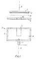
- Figure 1 is a schematic cross-section of one simple electronic display device in accordance with the present invention;
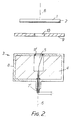
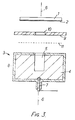
- Figures 2 and 3 illustrate modifications of the device illustrated in Figure 1, like references being used for like parts in Figures 1 to 3;
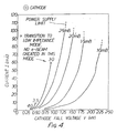
- Figures 4 and 5 are explanatory graphs;
- Figure 6 shows, in longitudinal cross-section, another example of an electron beam device in accordance with the present invention;
- Figure 7 is a schematic cross-section through a flat screen cathode ray display device in accordance with the present invention;
- Figure 8 illustrates in perspective part of the insulating
slab 20 of Figure 7; - Figure 9 illustrates, part broken away, one elongate anode member A used in the device of Figure 7;
- Figure 10 illustrates, part broken away, one elongate cathode member C utilised in Figure 7;
- Figure 11 is a perspective view, part broken away, of an assembly of cathode and anode members with the slab of insulating material shown in Figure 8 sandwiched therebetween;
- Figure 12 is a schematic diagram illustrating the operation of the device illustrated in Figures 7 to 11;
- Figure 13 is a schematic cross-section through another flat screen cathode ray device in accordance with the present invention;
- Figure 14 illustrates in perspective part of the device of Figure 13;
- Figure 15 illustrates in perspective part of the device of Figure 13; with like references being used for like parts;
- Figure 16 is a schematic cross-section of a display device in accordance with the invention;
- Figure 17 is a schematic cross-section of another display device in acordance with the invention;
- Figure 18 is a perspective view, part broken away, and
- Figure 19 a cross-sectional view, of yet another device in accordance with the invention;
- Figure 20 shows a longitudinal section of a further apparatus in accordance with the invention;
- Figure 21 is a longitudinal section of another apparatus in accordance with the invention;
- Figure 22 illustrates a thyratron in accordance with the invention;
- Figure 23 illustrates another thyratron in accordance with the invention;
- Figure 24 shows yet another thyratron in accordance with the invention;
- Figure 25 illustrates a cathode member in accordance with the invention;
- Figure 26 shows another cathode member; and
- Figure 27 illustrates another device in accordance with the invention.
- Referring to Figure 1, a device comprises a quartz envelope of which only one
portion 1 is shown. Theenvelope portion 1 is provided as a faceplate having on its interior alayer 2 of phosphor material similar to that used in conventional cathode ray display tubes. Associated with thephosphor layer 2 is a transparent metal layer (not shown but somewhat akin to the transaparent metal layer forming part of the screen of a conventional cathode ray tube) between thelayer 2 and the faceplate. The faceplate formed by theportion 1 of the envelope of the device is transparent. - Within the envelope and at the end thereof opposite to the
faceplate portion 1, is acathode member 3 which comprises ablock 4 of Kovar having ablind hole 5 formed therein, in this case by drilling coaxially with the axis ofcylindrical symmetry 6 of the device. The open mouth of thehole 5 faces thephosphor layer 2. In the base of theblock 4, adjacent the blind end of thehole 5, a connectingpin 7 is inserted so as to enable electrical connection to be made to theKovar block 4. - All of the external surfaces of the
Kovar cathode block 4, with the exception of the wall and base surfaces of theblind hole 5, which would otherwise be exposed to a gas filling within the envelope of the device are covered by electrically isolating material represented at 8. In this example, the insulatingmaterial 8 is glass. - Between the
cathode 3 and thephosphor layer 2 is ananode electrode 9 which has acircular hole 10 passing therethrough.Circular hole 10 is coaxially aligned with theblind hole 5 within theKovar block 4. - It will be noted that the
cathode 3 is devoid of a heater as such, or any electron emissive cathode material, such as barium. - The envelope of the tube is filled with helium at a pressure of between 0.2 and 10 mB.
- As so far described the device is in its simplest form. For the moment it will be assumed that
grid 11, shown between theanode electrode 9 and thephosphor layer 2, is absent. - Provided that the dimensions of the cathode and
anode holes anode 9 to thecathode 3 is suitably chosen, a type of electrical discharge will be established between theanode 9 and thecathode 3 which results in the formation of an electron beam along theaxis 6 of the coaxially aligned anode and cathode holes when a potential difference in the range of from several hundred volts to several thousand volts is established between theanode 9 and theblock 4 ofcathode 3. Within limits, the electron beam acquires energy approximately equal to the anode to cathode potential difference and so extends into the region beyond theanode hole 10 to impinge, finally, upon thephosphor layer 2 thus exciting it. - Thus, in operation, whenever a potential as aforesaid is established between
anode 9 and block 4 ofcathode 3, the resulting electron beam causes a spot to appear on thescreen 1 due to excitation of thephosphor layer 2. Whilst the aforementioned dimensions and spacing may be arrived at empirically, in the particular example illustrated in Figure 1, the cathode and anode holes were of 5 mm diameter. With a gas filling of helium at a pressure of 2 mB and a potential difference betweenanode 9 andcathode 3 of approximately 1.5 kV, the device was found to operate with a spacing between the plane of theanode 9 and the surface of thephosphor layer 2 of up to a few centimetres, and a spacing between theanode 9 and thecathode 3 of at least 3 mm. With the above-mentioned potential difference of 1.5 kV the current drawn from the cathode, was of the order of 15 mA. - Reverting to the aforementioned grid 11 - by introducing a control grid, modulation of the intensity or energy of the electron beam arriving at the surface of the
phosphor layer 2 may be achieved by varying a potential applied to thegrid 11. Alternatively or additionally varying the potential between theanode 9 and thecathode 3 will produce or enhance a modulation effect but, of course, it is much less convenient to apply modulation at high potential. - Referring to Figure 2, the essential difference between the device shown in Figure 2 and the device shown in Figure 1 resides in the fact that a mesh grid such as 11 in Figure 1 is not provided betwen the
anode 9 and thephosphor layer 2. Instead, a ring grid 11' is provided within the mouth of theblind hole 5 in theKovar block 4. Electrical connection is made to the ring grid 11' by means of a connector passing out through the base of theKovar block 4. In fact, instead of apin 7 making contact with theblock 4 the contact, here referenced 7' is cylindrical with the connecting lead for the grid 11' passing coaxially therethrough in insulated fashion. Although not shown in Figure 2, insulating material would be provided to support the connecting lead for thegrid 11 within the cylindrical connector 7'. - Referring to Figure 3, in this case, compared to Figure 1, the position of the
grid 11 is changed. Instead of providing this betweenanode 9 and thephosphor layer 2 it is provided between theanode 9 and thecathode 3. In some cases this may be preferred since a relatively lower voltage is required compared to that required with the grid in the position shown in Figure 1. - The graph of Figure 4 shows the relationship between beam current I and cathode fall voltage V (i.e. the voltage applied between anode and cathode) for different gas filling pressures, for a device as described above having cathode and anode holes of 5 mm in diameter.
- In any of the embodiments described above with reference to Figures 1, 2 and 3, instead of a single cathode hole and a single anode hole a plurality of blind holes may be provided in the
Kovar block 4 with each cathode hole being coaxially aligned with a corresponding hole passing through theanode member 9. Typically in such a case, the holes will be arranged in a ring formation, with or without cathode and anode holes on-centre. THe effect achieved using a plurality of cathode and anode holes in a simple device as illustrated in Figures 1 to 3, is that the areas of excitation thus created in thephosphor layer 2 tend to merge to produce a larger illuminated spot (or other prescribed pattern as determined by the pattern of holes on the faceplate 1) than would otherwise be the case. - The graph of Figure 5 shows parameters for this last-mentioned case corresponding to those shown in the graph of Figure 4 for this embodiment shown in Figure 1.
- One application for a device as described above is in large area displays such as those sometimes found in public places in order to impart information, e.g. in airport terminals or sports areas. By arranging devices such as those described above in rows and columns and addressing individual devices appropriately, letters and words - and even graphics - may be produced.
- Referring to Figure 6, another device in accordance with the invention includes a
glass envelope 12 which is of generally circular cross-section and has a transversely extending side-arm 13 about mid-way along its length. Ananode member 14 extends through the end wall of the side-arm 13 and into the main part of the volume enclosed by theenvelope 12. - A
cathode member 15 passes through an end wall of theenvelope 12. It has a stem portion 15A and anenlarged end 15B with ablind hole 16 of circular cross-section in its front surface. All of the surfaces of thecathode member 15 contained within theenvelope 12, except for the side wall and base surfaces of thehole 16, are coated with a layer ofglass 17. Theenvelope 12 contains helium at a pressure of 2 mB. - In operation, a potential difference of about 1 kV is applied across the anode and
cathode members hole 16. - The
envelope 12 has a length of about 7 cm and a diameter of about 3.5 cm. - The anode and
cathode members hole 16 is 5 mm, with a depth (i.e. axial length) of 3 mm. - Referring to Figures 7 to 11 a display device comprises a plurality of elongate cathode members C1 to C4 arranged parallel to one another to form a grid. Each cathode member, as shown in Figure 10, comprises a bar of Kovar having at regular intervals along its length blind holes 18. The
holes 18 extend into the same planar surface of the cathode member. Each cathode member is provided with an electrical connector (not shown) by means of which it may be individually addressed. - Superimposed above the grid of cathode members is a grid of parallel elongate anode memebers A1 to A5 each of which consists of a bar of Kovar having a series of
holes 19 passing therethrough from one planar face to its opposite planar face as illustrated in Figure 9. The pitch of theholes 19 in an anode member corresponds to the spacing between the cathode members in the cathode grid and the spacing of the anode members in the anode grid corresponds to the pitch of the cathode holes 18 in a cathode member so that eachcathode hole 18 is aligned with ananode hole 19 at the crossing point of the anode and cathode conductors in which those particular holes appear. - Sandwiched between the grid of cathode members and the grid of anode members is a
slab 20 of glass which has rows and columns ofholes 21 therein extending from one major planar face to its opposite major planar face, as illustrated in Figure 8. The rows and columns of holes are spaced such that when the slab is sandwiched between the grid of cathode members and the grid of anode members, as shown in Figure 11, each aligned cathode and anode hole at the crossing point of an anode and cathode member is also aligned with a hole in the slab of insulatingmaterial 20. Thus, theholes 21 in the insulatingslab 20 permit communication between appropriate ones of the cathode and anode holes 18 and 19 but impede communication between each cathode hole and other than the anode holes with which it is directly aligned. Thus the tendency for so-called "long path" discharges to take place is reduced. - Superimposed over the grid of anode members is a phosphor screen comprising of a layer of
phosphor material 22 on the inside of part of an enclosing envelope which is formed as afaceplate 23. Associated with thelayer 22 of phosphor material is a transparent layer of conductive material (somewhat akin to the transparent metal layer of the phosphor screen of a conventional cathode ray tube device) between thephosphor layer 22 and thefaceplate 23. The envelope in this case is of glass and encloses the anode and cathode members together, of course, with the interposed slab of insulatingmaterial 20. - The envelope has a gas filling of helium and, as illustrated only in Figure 7, each cathode member C is entirely covered with an electrically isolating
layer 24 of glass, except within theholes 18. Thus, save for the wall and base surfaces of theholes 18 all surfaces of the cathode members which would otherwise be exposed to the helium gas filling are isolated therefrom. In fact, save for the interior surfaces of theholes 18 as aforesaid, all surfaces at cathode potential are so isolated from the gas filling. In this particular case the wall and base surfaces of theholes 18 are entirely free from glass. In this particular example the cathode and anode holes 18 and 21 are of circular cross-section with a diameter of 5 mm. The helium gas filling is at a pressure of 2 mB. The distance separating the grid of cathode members from the grid of anode members (i.e. the thickness of the slab 20) is a few millimetres whilst the distance separating the grid of anode members from thephosphor layer 22 is in the region of 0.5 to 2 cm. - If now, and referring particularly to Figure 12, a 1.5 kV potential difference is established between cathode member C2 and anode member A4 than en electron beam will be formed in the region of the crossing point of members C2 and A4 which beam extends from out of the mouth of the
cathode hole 18 at the crossing point through the corresponding hole in the insulatingslab 20 to penetrate through the correspondinganode hole 19 in anode members A4 and impinge upon the phosphor screen to form a spot as represented at S in Figure 12. By addressing different combinations of anode members and cathode members corrresponding spots may be caused to appear on the screen at any of the crossing points and by suitably changing the combination of crossing points selected an animated display may be achieved. - No mention has so far been made of
grid 25 shown in Figure 7 as located between the grid of anode members A and thephosphor layer 22. The purpose of this grid, if provided, is to modulate the intensity or energy of the electron beams arriving at the phosphor. - Alternatively, with or without the
grid 25, the overall intensity or energy of the electrons beams may be modulated or adjusted by appropriate alterations to the anode to cathode discharge current as determined by the voltage applied between the cathode and anode members. - In another embodiment a
grid 26 is embedded in theslab 20, as shown in Figures 13 and 14, and may comprise a gauze or as metal plate having holes which correspond to the anode and cathode holes, as illustrated in Figure 15. - It will be noted particularly the absence of any form of conventional electron gun. No cathode heaters are employed in the device illustrated, the cathodes being cold cathodes, and no cathode material such as barium is employed.
- With reference to Figure 16, another embodiment of the invention includes a
cathode member 27 of Kovar having ahole 28 of about 5 mm diameter in its front surface and being enclosed in aglass envelope 29 which also contains helium gas at a pressure of about 2 mB and has a layer of phosphor on its inner surface to form ascreen 30. The surfaces of thecathode member 27, except the side wall and base of thehole 28, are covered in aglass layer 31, which electrically insulates thecathode member 27 from the helium gas filling. Electrical connection to thecathode member 27 is made via apin 32 which is sheathed with alayer 33 of glass. - An
anode member 34 is located between the front surface of thecathode member 27 and thephosphor screen 30, being about 2 cm from thecathode member screen 30. Theanode member 34 is also offset from the axis X-X of thehole 28, being about 2 cm to the right as shown. - When a 1.5 kV potential difference is established between the
cathode member 27 and theanode member 34, an electron beam is formed along the axis X-X of the hole, even though theanode member 34 is offset from that axis. The electron beam impinges on thephosphor screen 30 to form a spot. - The intensity of the spot may be varied by modulating the voltage applied to a
grid electrode 35, shown in this embodiment to be positioned between thescreen 30 and theanode member 34, although it could be located between the anode andcathode members - A further embodiment of the invention is illustrated schematically in Figure 17. A
cathode member 36 of Kovar has ahole 37 in its front surface and is coated with an electrically insulating layer of glass 38. Thecathode member 36 is contained within aglass envelope 39 having on its inner surface a layer of phosphor which acts as ascreen 40, and enclosing helium gas at 2 mB pressure. Thecathode member 36 is electrically connected via apin 41, which is also coated inglass 42, forming a stem. In this embodiment aKovar anode member 43 is located behind the front surface of thecathode member 36 and is positioned co-axially with it about thepin 41. - When in operation a potential difference of 1.5 kV is applied between the cathode and
anode members hole 37 and impinges on thescreen 40. - As in the previously described embodiments, a modulating grid may also be included, and/or modulation may be carried out by varying the potential difference applied.
- The
hole 37 has a diameter of about 5 mm and the front surface of thecathode member 36 may be between a few millimetres and a few centimetres from thescreen 40. - Yet another embodiment of the invention is now described with reference to Figures 18 and 19. A plurality of Kovar strips, only two of which 44 and 45 are shown, are arranged parallel to each other on a
glass slab 46. Each of the strips has a plurality of apertures through it, only four of which, 47, 48, 49 and 50; 51, 52, 53 and 54 are shown for each strip. Each strip forms an anode member, electrical signals being applied to them viarods -
Cathode members 57 to 64 are of Kovar and have stems extending through the apertures in thestrips glass slab 46. The surfaces of each cathode member, including the connecting pin comprising its stem, are coated in glass layers 65 and 66 except for the side wall and base of the single hole in each ones front surface. - The ends of the
cathode members 57 to 64 on the side of theglass slab 46 other than the anode strips 44 and 45 are connected viarods - By placing the structure within an envelope filled with helium at 2 mB pressure, and having a phosphor screen on its inner surface, a display may be produced.
- The front surfaces of the
cathode members 57 to 64 may be as litle as 5 mm from the surface of the screen, and a potential difference between the anode and cathode members of 1.5 kV would be required. - With reference to Figure 20, a thorated
tungsten cathode member 71 has a stem 72 via which electrical connection is made, and is covered with alayer 73 of electrically insulating glass which also extends to the stem 72. Ananode member 74 surrounds and is coaxial with the stem 72. - The
cathode member 71 has afront surface 75 in which is formed ablind hole 76 of circular cross-section, being 5 mm deep and having a diameter of about 1.5 mm, and having surfaces which are free of thelayer 73 of glass. Thefront surface 73 is inclined with respect to thehole 76 such that the longitudinal axis of thehole 76, shown as brokenline 77, is oblique to the normal 78 of thefront surface 75 at that point, the angle between them being about 3Oo. - The cathode and anode arrangement is enclosed within a glass envelope which also contains a gas filling of deuterium at about 2 mB pressure.
- In operation, when a suitably high voltage, say 2 kV, is established between the anode and the
cathode members hole 76 and normal to thefront surface 75. If, as illustrated awall 79, which might be for example the wall of the envelope or some other obstruction, is present, this could restrict the space available to the arrangement. By giving a suitable incline to thefront surface 75 thehole 76 can have a depth which might not be possible if itslongitudinal axis 77 were arranged to be parallel to the normal 78 to thefront surface 75. - With reference to Figure 21, a thorated
tungsten cathode member 80 is connected to stem 81 and is contained within an envelope (not shown) together with a deuterium gas filling at about 2 mB pressure and ananode member 82, which is coaxial with and surrounds thestem 81. - The
cathode member 80 and stem 81 are coated with alayer 83 of glass which electrically insulates them from the deuterium gas filling. - A plurality of
holes 84 are formed in afront surface 85 of thecathode member 80, each of them being of circular cross-section with a diameter of about 1.5 mm and a depth of 5 mm and having surfaces which are free of thelayer 83 of glass. Thefront surface 85 is curved, for example, it may be parabolically or spherically shaped, rather than theflat surface 75 shown in Figure 20. - In operation, when a voltage of about 2 kV is applied between the cathode and
anode members 80 and 82 a plurality of electron beams are formed extensive normal to thefront surface 85 at and in diretions away from respective holes, and come to a focus at apoint 86 which is located according to the configuration of thefront surface 85. - Although the
holes 84 are illustrated as being disposed mutually parallel, they could be arranged in some other way, since their attitude does not affect the directions of the electrons beams which are formed during operation. - Apparatus according to the invention in which the surface is curved to produce such focussing might find application in an electron beam welder, for example, in which case the piece being welded may also be for example contained within the envelope. It might also find application in the production of a point source of soft X-rays, having a wavelength of about 6.1O-1Om, for use in spectroscopy for example, or to generate a point source of incandescent black body radiation.
- With reference to Figure 22, a thyratron in accordance with the invention includes a
glass envelope 87, containing a gas filling, ananode 88, a screen grid 89 and control grids 9O and 91, such as might be found in a conventional thyratron. However, instead of the conventionally provided heated cathode, the cathode comprises acathode member 92 of tungsten having a plurality ofholes 93 in itsfront surface, facing theanode 88. The surface of thecathode member 92 is entirely covered with aglass layer 94 except for the walls and bases of theholes 93. When the thyratron is required to become conducting a suitably high voltage is applied between theanode 88 and thecathode member 92 such that an electron beam is formed extensive in a direction away from each hole. The gas filling becomes ionized and a conduction path is established between theanode 88 andcathode member 92. - Referring to Figure 23, another thyratron in accordance with the invention includes a
glass envelope 95 containing a gas filling, ananode 96, a screen grid 97 andcontrol grids heater filament 101. - Two
cathode members glass envelope 95. Each has ahole glass layer holes cathode members cathode members stem portions 108 and 109 which are surrounded bycoaxial anode members 110 and 111 respectively. - During operation of the thyratron, the
thermionic material 100 is heated by theheater filament 101 causing electrons to be emitted from its surface. The emitted electrons ionize that part of the gas filling between thecontrols grids control grids cathode members cathode members 110 and 111 respectiovely, such that electrons beams are formed extensive of theholes cathode members broken lines control grids - The cathode members could be located elsewhere within the
envelope 95 if it is desired to promote ionization in other regions of the thyratron, and of course only one, or more than two cathode members could be used. - With reference to Figure 24, another thyratron includes a glass envelope 114, gas filling, an
anode 115, ascreen grid 116 andcontrol grids thermionic cathode 119 having thermionic material 12O carried by asubstrate 121 of high thermal conductivity which may be nickel, for example. Acathode member 122 of tungsten is positioned on the substrate side of the cathode 12O. Thecathode member 122 has a plurality ofholes 123 in its front surface which is concave. The surface of thecathode member 122, except for the walls and bases of theholes 123, are covered with alayer 124 of glass. Ananode member 125 surrounds thecathode member 122. - In operation, a voltage is applied between the
anode member 125 and thecathode member 122 such that a beam of electrons is formed extensive of each hole. The curved surface of theblock 122 gives a focussing effect, and the electrons are directed to impinge on thesubstrate 121, their kinetic energy being converted into heat. Heat is conducted to the thermionic material 12O causing electrons to be emitted to produce ionization of the gas filling. - With reference to Figure 25, a cathode member is formed by inserting a tungsten
cylindrical rod 126 into ahollow tube 127 of an electrically insulating material, such as a ceramic or galss. - Figure 26 illustrates another cathode member in which a
tungsten rod 128 is inserted into ahollow metal tube 129, which may also be of tungsten, and a ceramic tube 13O is fitted over themetal tube 129. Any metal surfaces which would be exposed in use to a gas filling may then be covered with an insulating layer. By employing cathode members of this type no drilling is required, as it is with those previously described. - With reference to Figure 27, a device in accordance with the invention comprises within an envelope (not shown) which also contains a gas filling, a
cylindrical cathode member 131 having astem portion 132 via which electrical connection is made to thecathode member 131. Thecathode member 131 has afront surface 132 of circular transverse cross-section which is of a 'dished' or frusto-conical configuration, the front surface being inclined such that the length of thecathode member 131 along its axis Z-Z increases from its centre to its circumference. Other surface configuration may of course be employed if desired. Ahole 133 is located in the centre of thefront surface 132 and is coaxial with axis Z-Z of thecathode member 131. The surfaces of thecathode member 131 and thestem portion 132 are covered with alayer 134 of electrically insulating glass,and ananode member 135 surrounds and is coaxial with thestem portion 132. - When a voltage is applied between the
cathode member 131 and theanode member 135 an electron beam is formed extensive of thehole 133. The beam is formed in a direction normal to thefront surface 132. Since at the edge of thehole 133 thefront surface 132 is inclined, components of the beam at points around the edge of thehole 133 are directed towards the axis Z-Z, such that the beam is brought to a focus F. The position of the focus F depends on the amount of inclination of the front surface. Such a device may thus produce a lens-like action, without the need for electron lens. - If the front surface is flat then a beam is produced which, although it is highly collimated, tends to diverge to some extent because of, for example, scattering processes. By using a front surface having a small degree of dishing, this tendency may be counteracted.
Claims (61)
- Apparatus for forming an electron beam comprising, within an envelope, an anode member (9); a cathode member (3) of electrically conductive material; means for applying a voltage between the anode member (9) and cathode member (3); and a gas filling, and wherein, except for part of a front surface of said cathode member, substantially the whole of the surface of said cathode member which would otherwise be exposed to the gas filling within said envelope is covered with an electrically insulating material (8), the gas pressure, voltage and electrode arrangement being such that, upon the application of the voltage between said anode member (9) and said cathode member (3), a discharge is produced which is characterized by the formation of an electron beam extensive in a direction away from said part of said front surface.
- Apparatus as claimed in claim 1 wherein said part is a hole (5) in the said front surface, the whole arrangement being such that upon the application of a suitably high voltage between said anode member (9) and said cathode member (3) a highly directional electron beam is formed extensive in a direction away from said hole.
- Apparatus as claimed in claim 2 and wherein the anode member (9) is located in front of the front surface of the cathode member (3).
- Apparatus as claimed in claim 3 and including a control grid electrode (11) through which in operation the electron beam passes.
- Apparatus as claimed in claim 3 or 4 and including a plurality of elongate cathode members (C1 to C4) arranged in a grid formation, and a plurality of elongate anode members (A1 to A4) arranged in a grid formation with said grid of anode members superimposed over said grid of cathode members, but spaced therefrom, with said anode members in crossing relationship with said cathode members to form a matrix, each of said cathode members having a series of holes (18) entering into its surface facing said grid of anode members and each of said anode members having a series of holes (19) passing therethrough, with each hole in an anode member aligned with a hole in a different one of the cathode members, and all surfaces of said cathode members, except for the surfaces within said holes in said cathode members, which would otherwise be exposed to said gas filling are isolated therefrom by electrically insulating material (24), and the whole arrangement being such that by applying a high potential between one of said anode members and one of said cathode members an electron beam is formed at the crossing point of said last-mentioned two members, said electron beam being extensive in the space between the mouth of the hole in the cathode member at said crossing point and said anode member, said beam being arranged to penetrate through the corresponding hole in said addressed anode member.
- Apparatus as claimed in claim 5 and wherein insulating material (20) is interposed between said grid of cathode members and said grid of anode members, which insulating materal has passages therethrough aligned with said holes in said cathode and anode members whereby to permit communication between one cathode hole and appropriate anode hole but impede communication between that cathode hole and any other anode hole.
- Apparatus as claimed in claim 6 and wherein said interposed insulating material is provided in the form of a slab having holes (21) extending beween its major surfaces and forming the said passages.
- Apparatus as claimed in claim 5, 6 or 7 and including a control grid electrode (25) located on the side of the grid of anode members other than that on which the grid of cathode members is located.
- Apparatus as claimed in claim 5, 6 or 7 and wherein a control grid electrode (26) is located between the grid of cathode members and the grid of anode members.
- Apparatus as claimed in claim 9 when dependent on claim 6 or 7 and wherein the grid electrode is embedded in the interposed insulating material.
- Apparatus as claimed in claim 2 and wherein the anode member (14) is located to one side of the axis of the electron beam formed in operation.
- Apparatus as claimed in claim 2 and wherein the anode member (43) is located behind said front surface of the cathode member (36).
- Apparatus as claimed in claim 12 and wherein the anode member (43) is co-axial with the cathode member (36).
- Apparatus as claimed in claim 12 or 13 and including a grid electrode through which in operation the electron beam passes.
- Apparatus as claimed in claim 12, 13 or 14 and wherein there are included a plurality of elongate anode members (44,45), each having apertures (47 to 54) therein; and a plurality of stemmed cathode members (57 to 64), each having a hole in the front surface thereof and arranged such that its stem extends through one of said apertures, such that each anode member is located behind the front surfaces of cathode members whose stems pass through apertures in said anode member, whereby by applying a high potential between an anode member and one of the cathode members extending through an aperture therein an electron beam is formed extensive in a direction away from the hole in said one of the cathode members.
- Apparatus as claimed in claim 15 and wherein a cathode member extending through an aperture in one anode member is electrically connected to another cathode member extending through an aperture in another anode member.
- Apparatus as claimed in claim 16 and wherein a connector connecting two cathode members is spaced from the anode members by electrically insulating material (46).
- Apparatus as claimed in any preceding claim and including a phosphor layer (22) arranged so that when an electron beam is formed it impinges upon a spot upon said layer whereby to excite the same.
- Apparatus as claimed in claim 18 and wherein said envelope has a portion formed as a faceplate on the interior of which said phosphor layer is provided.
- A video signal reproducing apparatus including apparatus as claimed in any preceding claim.
- Cathode ray tube apparatus comprising apparatus as claimed in claim 5 and including, superimposed over said grid of anode members on the side thereof remote from said grid of cathode members, a phosphor screen (22), such that, in operation, said beam penetrates through the corresponding hole in said addressed anode member to impinge upon a spot upon said phosphor screen whereby to excite the same.
- Apparatus as claimed in claim 2 and wherein the longitudinal axis (77) of said hole (76) is oblique to the normal (78) of said front surface, and the electron beam is formed normal to said front surface at said hole.
- Apparatus as claimed in claim 22 and including a plurality of holes (84) in said front surface, at least one of said holes having its longitudinal axis oblique to the normal of said front surface at that hole, such that upon the application of said suitably high voltage, electron beams are formed extensive normal to said front surface at and in a direction away from, respective holes.
- Apparatus as claimed in claim 23 and wherein said front surface (85) is curved.
- Apparatus as claimed in claim 1 or 2 wherein the front surface of the cathode member is curved (85), and, except for a plurality of discrete parts of the said front surface, substantially the whole of the surface of said cathode member which would otherwise be exposed to the gas filling within said envelope is covered with an electrically insulating material (83), the whole arrangement being such that upon the application of a suitably high voltage between said anode member and said cathode member electron beams are formed extensive normal to said front surface at and in a direction away from respective parts.
- Apparatus as claimed in claim 24 or 25 and wherein said front surface (85) is curved such that the electron beams formed are focussed at a point.
- Apparatus as claimed in claim 22, 23, 24, 25 or 26 and wherein said anode member (82) co-axially surrounds and is behind said front surface of said cathode member.
- Apparatus as claimed in claim 2 and including a layer (2) of phosphor material on a viewable screen arranged such that upon the application of said suitably high voltage the electron beam impinges upon said phosphor layer (2) and so excites the same.
- Apparatus as claimed in claim 28 and wherein said anode member (9) has an aperture (10) therein and is located between said cathode member (3) and said phosphor layer (2), said electron beam being arranged to penetrate through said aperture.
- Apparatus as claimed in claim 29 and wherein the hole in said cathode member and said aperture in said anode member are coaxially aligned.
- Apparatus as claimed in claim 28, 29 or 30 and wherein said envelope (1) has a portion formed as a faceplate upon the inner surface of which said phosphor layer (2) is provided.
- Apparatus as claimed in any of claims 28 to 31 including a modulating grid (11) provided to affect the strength or intensity of the electron beam impinging upon said phosphor layer.
- Apparatus as claimed in claim 32 and wherein said modulating grid (11) is a perforated grid or gauze provided between said anode member and said phosphor layer.
- Apparatus as claimed in claim 32 and wherein said modulating grid or gauze is provided between said anode member and said cathode member.
- Apparatus as claimed in claim 32 and wherein said modulating grid comprises a ring grid (11') provided within the mouth of said hole (5) in said cathode member.
- Apparatus as claimed in claim 35 and wherein an electrical connection for said grid is taken out, in insulated fashion, through said cathode member in a direction away from said anode member.
- Apparatus as claimed in any of claims 28 to 36 wherein electrical connection to said cathode member is provided for by means of a first electrical connector connected to the base of said cathode member.
- Apparatus as claimed in claim 37 and wherein said first electrical connector is preferably in the form of a hollow cylinder.
- Apparatus as claimed in claim 38 and wherein, where said modulating grid comprises a ring grid provided within the mouth of said hole in said cathode member and an electrical connection for said grid is taken out, in insulated fashion, through said cathode member in a direction away from said anode member, a second electrical connector for said grid passes through said hollow cylinder.
- Apparatus as claimed in any of claims 28 to 39 wherein a plurality of holes (18) are provided in said cathode member (C) and a corresponding plurality of holes (19) are provided in said anode member (A).
- Display apparatus comprising apparatus as claimed in claim 1 or 2 and including within the envelope, a layer of phosphor material on a viewable screen; the cathode member being remote from said phosphor layer (22) and the anode electrode being apertured and located between said cathode member and said phosphor layer and, in operation, the electron beam being arranged to penetrate through an aperture in said anode member to impinge upon said phosphor layer and so excite the same.
- Thyratron apparatus comprising apparatus as claimed in claim 1 or 2.
- Apparatus as claimed in claim 42 and wherein said cathode member (92) has a plurality of holes (93) in the front surface thereof, such that upon application of a suitably high voltage, electron beams are formed extensive in a direction away from respective holes.
- Apparatus as claimed in claim 43 and wherein said front surface is curved.
- Apparatus as claimed in claim 44 and wherein at least one of said holes (123) has its longitudinal axis oblique to the normal of said front surface at that hole.
- Apparatus as claimed in any of claims 42 to 45 and including thermionic material (120) arranged such that when an electron beam, or beams are formed they heat the same.
- Apparatus as claimed in claim 42 and wherein, when said electron beam (112,113) is formed it is arranged to ionize the gas filling in a localised region.
- Apparatus as claimed in claim 47 and wherein the longitudinal axis of said hole (104,105) is oblique to the normal of said front surface at the hole.
- Apparatus as claimed in claim 2 and wherein said front surface (132) is shaped to focus said electron beam.
- Apparatus as claimed in claim 2 or 49 and wherein said front surface is substantially frusto-conical, the hole (133) being centrally located.
- Apparatus as claimed in any of claims 2 to 50 and wherein the or each hole (5) in a cathode member is blind.
- Apparatus as claimed in any of claims 2 to 51 and wherein the or each hole (5) in a cathode member is of circular cross-section.
- Apparatus as claimed in any of claims 2 to 52 and wherein the side wall and base surfaces of the or each hole in a cathode member is entirely free of a covering of electrically insulating material.
- Apparatus as claimed in any preceding claim and wherein said insulating material (8) insulating surfaces of said cathode member or plurality of cathode members from said gas filling is glass.
- Apparatus as claimed in any preceding claim and wherein said cathode member (3), or plurality of cathode members, is of Kovar (Trade Mark).
- Apparatus as claimed in any preceding claim and wherein said anode member (9), or plurality of anode members, is of Kovar (Trade Mark).
- Apparatus as claimed in any preceding claim, and wherein said envelope (1) is of glass.
- Apparatus as claimed in any preceding claim and wherein the said gas filling is helium.
- Apparatus as claimed in any preceding claim and wherein said gas filling is at a pressure of between 0.5 and 2.5 mB.
- Apparatus as claimed in any preceding claim and wherein the high voltage applied between the anode member and the cathode member is between 1 and 2.5 kV.
- Apparatus as claimed in any preceding claim and wherein said cathode member is of thorated tungsten.
Priority Applications (1)
| Application Number | Priority Date | Filing Date | Title |
|---|---|---|---|
| AT84308798T ATE79979T1 (en) | 1983-12-20 | 1984-12-17 | ELECTRON BEAM GENERATOR. |
Applications Claiming Priority (8)
| Application Number | Priority Date | Filing Date | Title |
|---|---|---|---|
| GB8333880 | 1983-12-20 | ||
| GB8333879 | 1983-12-20 | ||
| GB8333880 | 1983-12-20 | ||
| GB8333879 | 1983-12-20 | ||
| GB8413791 | 1984-05-30 | ||
| GB848413791A GB8413791D0 (en) | 1983-12-20 | 1984-05-30 | Forming electron beams |
| GB8431116 | 1984-12-10 | ||
| GB08431116A GB2153140B (en) | 1983-12-20 | 1984-12-10 | Apparatus for forming electron beams |
Publications (3)
| Publication Number | Publication Date |
|---|---|
| EP0146383A2 EP0146383A2 (en) | 1985-06-26 |
| EP0146383A3 EP0146383A3 (en) | 1987-04-01 |
| EP0146383B1 true EP0146383B1 (en) | 1992-08-26 |
Family
ID=27449524
Family Applications (1)
| Application Number | Title | Priority Date | Filing Date |
|---|---|---|---|
| EP84308798A Expired EP0146383B1 (en) | 1983-12-20 | 1984-12-17 | Apparatus for forming electron beams |
Country Status (3)
| Country | Link |
|---|---|
| US (1) | US4698546A (en) |
| EP (1) | EP0146383B1 (en) |
| DE (1) | DE3485897T2 (en) |
Families Citing this family (20)
| Publication number | Priority date | Publication date | Assignee | Title |
|---|---|---|---|---|
| US4825446A (en) * | 1986-06-14 | 1989-04-25 | English Electric Valve Company Limited | Laser apparatus having cathode bore directing electron beam onto anode |
| GB8614541D0 (en) * | 1986-06-14 | 1986-07-23 | English Electric Valve Co Ltd | Electron beam apparatus |
| GB2194673B (en) * | 1986-08-30 | 1990-10-24 | English Electric Valve Co Ltd | Apparatus for forming an electron beam sheet |
| EP0259045A3 (en) * | 1986-08-30 | 1989-10-25 | English Electric Valve Company Limited | Gas discharge devices |
| US5686789A (en) * | 1995-03-14 | 1997-11-11 | Osram Sylvania Inc. | Discharge device having cathode with micro hollow array |
| US6016027A (en) * | 1997-05-19 | 2000-01-18 | The Board Of Trustees Of The University Of Illinois | Microdischarge lamp |
| JP4907760B2 (en) * | 2000-11-15 | 2012-04-04 | 浜松ホトニクス株式会社 | Gas discharge tube |
| US6563257B2 (en) | 2000-12-29 | 2003-05-13 | The Board Of Trustees Of The University Of Illinois | Multilayer ceramic microdischarge device |
| US7112918B2 (en) * | 2002-01-15 | 2006-09-26 | The Board Of Trustees Of The University Of Illinois | Microdischarge devices and arrays having tapered microcavities |
| US6843897B2 (en) * | 2002-05-28 | 2005-01-18 | Applied Materials, Inc. | Anode slime reduction method while maintaining low current |
| US6855235B2 (en) * | 2002-05-28 | 2005-02-15 | Applied Materials, Inc. | Anode impedance control through electrolyte flow control |
| US20050092602A1 (en) * | 2003-10-29 | 2005-05-05 | Harald Herchen | Electrochemical plating cell having a membrane stack |
| US7511426B2 (en) * | 2004-04-22 | 2009-03-31 | The Board Of Trustees Of The University Of Illinois | Microplasma devices excited by interdigitated electrodes |
| US7385350B2 (en) * | 2004-10-04 | 2008-06-10 | The Broad Of Trusstees Of The University Of Illinois | Arrays of microcavity plasma devices with dielectric encapsulated electrodes |
| US7573202B2 (en) * | 2004-10-04 | 2009-08-11 | The Board Of Trustees Of The University Of Illinois | Metal/dielectric multilayer microdischarge devices and arrays |
| US7297041B2 (en) * | 2004-10-04 | 2007-11-20 | The Board Of Trustees Of The University Of Illinois | Method of manufacturing microdischarge devices with encapsulated electrodes |
| US7477017B2 (en) * | 2005-01-25 | 2009-01-13 | The Board Of Trustees Of The University Of Illinois | AC-excited microcavity discharge device and method |
| US12397363B2 (en) | 2011-03-31 | 2025-08-26 | Norsk Titanium As | Method and arrangement for building metallic objects by solid freeform fabrication |
| GB2489493B (en) | 2011-03-31 | 2013-03-13 | Norsk Titanium Components As | Method and arrangement for building metallic objects by solid freeform fabrication |
| EP3481579A1 (en) | 2016-07-08 | 2019-05-15 | Norsk Titanium AS | Method and arrangement for building metallic objects by solid freeform fabrication with two welding guns |
Family Cites Families (19)
| Publication number | Priority date | Publication date | Assignee | Title |
|---|---|---|---|---|
| NL67662C (en) * | 1943-11-08 | |||
| GB763670A (en) * | 1953-08-14 | 1956-12-12 | Standard Telephones Cables Ltd | Improvements in or relating to thermionic cathodes |
| BE531122A (en) * | 1953-08-14 | |||
| US3262008A (en) * | 1963-11-12 | 1966-07-19 | Bendix Corp | Bistable device |
| SE321533B (en) * | 1965-04-12 | 1970-03-09 | Asea Ab | |
| GB1357535A (en) * | 1970-10-06 | 1974-06-26 | Emi Ltd | Spectroscopic lamps |
| NL7016929A (en) * | 1970-11-19 | 1972-05-24 | ||
| GB1404897A (en) * | 1973-04-05 | 1975-09-03 | Oki Electric Industry Co Ltd | Cold cathode discharge type display devcies and method for the production thereof |
| US3967150A (en) * | 1975-01-31 | 1976-06-29 | Varian Associates | Grid controlled electron source and method of making same |
| FR2352390A1 (en) * | 1976-05-21 | 1977-12-16 | Thomson Csf | LOW ENERGY ELECTRON DISPLAY SYSTEM WITH MEMORIZATION, AND FLAT SCREEN DEVICES FOR DATA DISPLAY AND TELEVISION |
| GB1568506A (en) * | 1978-03-09 | 1980-05-29 | English Electric Valve Co Ltd | Laser arrangements |
| US4196938A (en) * | 1978-06-07 | 1980-04-08 | Blokin Vladimir I | Gas-discharge chamber electrode and electrode system using same |
| GB2023922B (en) * | 1978-06-19 | 1982-11-24 | Lunev E | And others gas discharge electrodes |
| DE3067141D1 (en) * | 1979-08-16 | 1984-04-26 | Tokyo Shibaura Electric Co | Flat display device |
| JPS5769645A (en) * | 1980-10-17 | 1982-04-28 | Fujitsu Ltd | Gas discharge panel |
| JPS57119436A (en) * | 1981-01-16 | 1982-07-24 | Nec Corp | Impregnated type cathode |
| JPS57208040A (en) * | 1981-06-18 | 1982-12-21 | Mitani Denshi Kogyo Kk | Graph display apparatus |
| JPS5830038A (en) * | 1981-08-17 | 1983-02-22 | Sony Corp | Discharge display unit |
| NL8200875A (en) * | 1982-03-04 | 1983-10-03 | Philips Nv | DEVICE FOR RECORDING OR PLAYING IMAGES AND SEMICONDUCTOR DEVICE FOR USE IN SUCH A DEVICE. |
-
1984
- 1984-12-17 EP EP84308798A patent/EP0146383B1/en not_active Expired
- 1984-12-17 DE DE8484308798T patent/DE3485897T2/en not_active Expired - Fee Related
- 1984-12-18 US US06/683,035 patent/US4698546A/en not_active Expired - Fee Related
Also Published As
| Publication number | Publication date |
|---|---|
| EP0146383A3 (en) | 1987-04-01 |
| EP0146383A2 (en) | 1985-06-26 |
| DE3485897D1 (en) | 1992-10-01 |
| US4698546A (en) | 1987-10-06 |
| DE3485897T2 (en) | 1993-01-07 |
Similar Documents
| Publication | Publication Date | Title |
|---|---|---|
| US4698546A (en) | Apparatus for forming electron beams | |
| AU2003235984B2 (en) | Gas discharge tube | |
| US3334269A (en) | Character display panel having a plurality of glow discharge cavities including resistive ballast means exposed to the glow discharge therein | |
| GB2153140A (en) | Apparatus for forming electron beams | |
| US3743879A (en) | Cold cathode display panel having a multiplicity of gas cells | |
| JP3292682B2 (en) | Gas discharge lamp filled with deuterium, hydrogen, mercury, metal halide or rare gas | |
| US4322659A (en) | Gas-discharge devices and display panels | |
| CA1278017C (en) | X-ray source | |
| US4213072A (en) | Gas discharge display device including web shaped spacing elements | |
| GB2074783A (en) | Mounting of a heat-shielded cathode in an electron gun | |
| CA1048182A (en) | Laser driven plasma display | |
| US4904900A (en) | Glow discharge lamp | |
| US5021708A (en) | Cathode for emission of electrons and electron tube with a cathode of this type | |
| EP0125859A1 (en) | Element | |
| US3099762A (en) | Cathode ray tube using replaceable cathode | |
| US2786957A (en) | Emissive cathodes | |
| EP0009962B1 (en) | Display arrangements | |
| KR100371040B1 (en) | Thin film display device | |
| US3821584A (en) | Gas filled display device having mercury inlet shield | |
| US4825446A (en) | Laser apparatus having cathode bore directing electron beam onto anode | |
| US4523124A (en) | Cathode-ray tube having multiplate cathode unit | |
| JPS6134837A (en) | Device for forming electron beam | |
| US3684909A (en) | Display panel having particle source | |
| US4758766A (en) | Gas discharge devices utilizing electron injection for gas ionization | |
| US2136292A (en) | Electric discharge device |
Legal Events
| Date | Code | Title | Description |
|---|---|---|---|
| PUAI | Public reference made under article 153(3) epc to a published international application that has entered the european phase |
Free format text: ORIGINAL CODE: 0009012 |
|
| AK | Designated contracting states |
Designated state(s): AT BE CH DE FR IT LI LU NL SE |
|
| PUAL | Search report despatched |
Free format text: ORIGINAL CODE: 0009013 |
|
| AK | Designated contracting states |
Kind code of ref document: A3 Designated state(s): AT BE CH DE FR IT LI LU NL SE |
|
| 17P | Request for examination filed |
Effective date: 19870706 |
|
| 17Q | First examination report despatched |
Effective date: 19880428 |
|
| RAP1 | Party data changed (applicant data changed or rights of an application transferred) |
Owner name: EEV LIMITED |
|
| GRAA | (expected) grant |
Free format text: ORIGINAL CODE: 0009210 |
|
| AK | Designated contracting states |
Kind code of ref document: B1 Designated state(s): AT BE CH DE FR IT LI LU NL SE |
|
| PG25 | Lapsed in a contracting state [announced via postgrant information from national office to epo] |
Ref country code: SE Free format text: THE PATENT HAS BEEN ANNULLED BY A DECISION OF A NATIONAL AUTHORITY Effective date: 19920826 Ref country code: NL Effective date: 19920826 Ref country code: LI Effective date: 19920826 Ref country code: IT Free format text: LAPSE BECAUSE OF FAILURE TO SUBMIT A TRANSLATION OF THE DESCRIPTION OR TO PAY THE FEE WITHIN THE PRESCRIBED TIME-LIMIT;WARNING: LAPSES OF ITALIAN PATENTS WITH EFFECTIVE DATE BEFORE 2007 MAY HAVE OCCURRED AT ANY TIME BEFORE 2007. THE CORRECT EFFECTIVE DATE MAY BE DIFFERENT FROM THE ONE RECORDED. Effective date: 19920826 Ref country code: CH Effective date: 19920826 Ref country code: BE Effective date: 19920826 Ref country code: AT Effective date: 19920826 |
|
| REF | Corresponds to: |
Ref document number: 79979 Country of ref document: AT Date of ref document: 19920915 Kind code of ref document: T |
|
| REF | Corresponds to: |
Ref document number: 3485897 Country of ref document: DE Date of ref document: 19921001 |
|
| REG | Reference to a national code |
Ref country code: CH Ref legal event code: PL |
|
| ET | Fr: translation filed | ||
| PG25 | Lapsed in a contracting state [announced via postgrant information from national office to epo] |
Ref country code: LU Free format text: LAPSE BECAUSE OF NON-PAYMENT OF DUE FEES Effective date: 19921231 |
|
| NLV1 | Nl: lapsed or annulled due to failure to fulfill the requirements of art. 29p and 29m of the patents act | ||
| PLBE | No opposition filed within time limit |
Free format text: ORIGINAL CODE: 0009261 |
|
| STAA | Information on the status of an ep patent application or granted ep patent |
Free format text: STATUS: NO OPPOSITION FILED WITHIN TIME LIMIT |
|
| 26N | No opposition filed | ||
| PG25 | Lapsed in a contracting state [announced via postgrant information from national office to epo] |
Ref country code: FR Effective date: 19930831 |
|
| PG25 | Lapsed in a contracting state [announced via postgrant information from national office to epo] |
Ref country code: DE Effective date: 19930901 |
|
| REG | Reference to a national code |
Ref country code: FR Ref legal event code: ST |