EP0143005B1 - Digital data converting methods and apparatus - Google Patents
Digital data converting methods and apparatus Download PDFInfo
- Publication number
- EP0143005B1 EP0143005B1 EP84308148A EP84308148A EP0143005B1 EP 0143005 B1 EP0143005 B1 EP 0143005B1 EP 84308148 A EP84308148 A EP 84308148A EP 84308148 A EP84308148 A EP 84308148A EP 0143005 B1 EP0143005 B1 EP 0143005B1
- Authority
- EP
- European Patent Office
- Prior art keywords
- converted
- signal
- words
- bits
- coded
- Prior art date
- Legal status (The legal status is an assumption and is not a legal conclusion. Google has not performed a legal analysis and makes no representation as to the accuracy of the status listed.)
- Expired - Lifetime
Links
Images


Classifications
-
- H—ELECTRICITY
- H03—ELECTRONIC CIRCUITRY
- H03K—PULSE TECHNIQUE
- H03K7/00—Modulating pulses with a continuously-variable modulating signal
-
- H—ELECTRICITY
- H03—ELECTRONIC CIRCUITRY
- H03M—CODING; DECODING; CODE CONVERSION IN GENERAL
- H03M7/00—Conversion of a code where information is represented by a given sequence or number of digits to a code where the same, similar or subset of information is represented by a different sequence or number of digits
- H03M7/14—Conversion to or from non-weighted codes
-
- G—PHYSICS
- G11—INFORMATION STORAGE
- G11B—INFORMATION STORAGE BASED ON RELATIVE MOVEMENT BETWEEN RECORD CARRIER AND TRANSDUCER
- G11B20/00—Signal processing not specific to the method of recording or reproducing; Circuits therefor
- G11B20/10—Digital recording or reproducing
- G11B20/14—Digital recording or reproducing using self-clocking codes
- G11B20/1403—Digital recording or reproducing using self-clocking codes characterised by the use of two levels
- G11B20/1423—Code representation depending on subsequent bits, e.g. delay modulation, double density code, Miller code
- G11B20/1426—Code representation depending on subsequent bits, e.g. delay modulation, double density code, Miller code conversion to or from block codes or representations thereof
Definitions
- This invention relates to digital data converting methods and apparatus.
- the methods and apparatus are suitable, for example, for use where an audio signal is pulse code modulated and then recorded.
- Apparatus in which an analog signal such as an audio signal is converted into a pulse code modulated (PCM) signal, magnetically recorded using a rotary head without forming guard-bands, and then reproduced.
- PCM pulse code modulated
- Such known apparatus in addition to a differentiated output characteristic of the magnetic recording and a low frequency cross-talk component generated from adjacent tracks, low frequency components are cut off by a rotary transformer, so the low frequency components of the audio signal cannot be reproduced with high fidelity.
- NRZI non-return to zero, inverted
- the modulated signal when consecutive digital zeroes appear, the modulated signal is not inverted during the period occupied by the digital zeroes, and the frequency of the modulated signal becomes low. Thus, the DC and the low frequency components are increased.
- bits (B 1 , B 2 , B 3 , B 4 , B 5 , B 6 , B 7 , B s ) of digital information in a base digital signal are converted to ten bits (P 1 , P 2 , P 3 , P 4 , P 5 , P s , P 7 , P s , Pg, P 10 ).
- Eight bits (B 1 , B 2 , B 3 , B 4 , B s , B s , B 7 , B 8 ) can be combined in 256(2 S ) different ways.
- T max /T min 4 (where T max is the maximum internal between levelal :ransistions and T min is the minimum interval between level transitions), a condition is required such that in n the NRZI-coding, the number of consecutive digital zeroes is less than three, or in the converted signal the number of consecutive bits of the same level is less than four.
- Table I shows the possible combinations of ten digital bits in the NRZI code for which the DC component is zero, but in which there are no more than three digital zeroes in a row (either internally of each 10-bit word or at the boundary between two such words):
- Table I shows that there are numerous possible combinations that will satisfy the constraints. For example, if up to three digital zeroes are permitted at the beginning of each word, then no digital zeroes can be permitted at the end of any word. In that case, Table I shows the total of the possible combinations is:
- the following table illustrates the number of possible 10-bit combinations, which begin with no more than two digital zeroes and end with no more than one digital zero, having a DC component of 0, -2 and +2 when NRZI-coded.
- the low frequency spectrum of the modulation wave tends to decrease more if the combination alternately using the combination with +2 and -2 DC component is used more frequently than the combinations with a zero DC component. Accordingly, 125 combinations with a pair of +2 and -2 DC components are used and the remaining 131 combinations with a zero DC component are used for 256 combinations of eight bit, by which 125 combinations and 131 combinations are made corresponding respectively to 256 combinations of eight bits.
- the pair may be selected such that DC component can be controlled only by changing the first bit (the second bit and the following bits in combinations of a pair are formed as the same level). Therefore, of the possible combinations in, for example, Table II, the combinations with +2 and -2 DC components and the first bit beginning with "0": are used. And, it is possible that 124 combinations and the combinations with a zero DC component, in this case, 132 combinations are made corresponding respectively to 256 combinations of eight bits. Then, each time the combination with ⁇ 2 DC components appears, the first bit of the combination is converted in such a manner that the DC component becomes positive and negative alternately.
- the DC component of each bit is generally called a digital sum variation (DSV), which is one of the evaluation methods.
- DSV digital sum variation
- DSV variance a parameter which is generally referred to as DSV variance.
- FIG. 5 of the accompanying drawings shows an example of an apparatus which is capable of conversion in accordance with the above converting system.
- the apparatus comprises an input terminal 1, an 8-bit shift register 2 which accepts information of eight bits, a conversion logic circuit 3 which uses, for example, a programmable logic array (PLA), and a clock terminal 4. Then, information applied to the input terminal 1 is transferred eight bits at a time through the shift register 2 in response to a pulse which is applied to the clock terminal 4 at the data bit rate, and the information of eight bits (B i , B 2 , B 3 , B 4 , B 5 , B o , B 7 , B s ) is supplied to the conversion logic circuit 3.
- PDA programmable logic array
- An identifying circuit 5 identifies whether the first bit is variable or fixed, namely, in this case, whether the DC component of the combination is "0" or +2.
- the identifying circuit 5 consists of, for example, exclusive-OR (hereinafter simply referred to as EOR) circuits 5a to 5c and an exclusive-NOR (hereinafter simply referred to as ENOR) circuit 5d.
- EOR exclusive-OR
- ENOR exclusive-NOR
- the circuits 5a to 5d carry out modulo addition of the even-numbered bits of the output from the conversion logic circuit 3. In other words, the identifying circuit 5 detects whether the number of digital zeroes of the even-numbered bits is even or odd.
- the identifying circuit 5 identifies that the combination has ⁇ 2 DC components and produces high level "1" at its output side, namely, the output side of the ENOR circuit 5d. That is, the identifying circuit 5 carries out all EOR logic operations of the even-numbered bit outputs of the output of the conversion logic circuit 3. In this case, when the even-numbered bit is "1", the level transition is carried out in this portion so that the DC components of this bit and the immediately preceding bit become 0. While, when the even-numbered bit is "0", there exist ⁇ 2 DC components. Further, when there are two digital zeroes, the DC component becomes 0 to ⁇ 4. In like manner, when there are three digital zeroes, the DC component be becomes ⁇ 2 or ⁇ 6.
- the whole of the DC component of ten bits is restricted to 0 or -2. Accordingly, by detecting whether the number of digital zeroes of the above even-numbered bit is even or odd, it is possible to identify whether the DC component is 0 or ⁇ 2.
- the output of the identifying circuit 5 is supplied to one input terminal of an AND circuit 6, and the AND circuit 6 is supplied at its other input terminal with an output from a detecting circuit 8 which is provided at the output side of the shift register 7 for detecting the DC component (DSV) of each combination.
- the detecting circuit 8 supplied the high level output to the input side of the AND circuit 6 when the DC component DSV' up to the preceding combination is, for example, -1.
- the output of the AND circuit 6 is supplied to one input terminal of an EOR circuit 11 which inverts the first bit level.
- To the other input terminal of the EOR circuit 11 is supplied the first bit P 1 of ten bits from the conversion logic circuit 3. Accordingly, when the output of the AND circuit 6 if "0", the first bit P 1 is not inverted in level and fed as it is to the shift register 7, while even when the output of the AND circuit 6 is "1", the first bit P 1 is inverted in polarity and fed to the shift register 7.
- an EOR circuit 9 and a D-type flip-flop circuit 10 constitute an NRZI-modulating circuit.
- the detecting circuit 8 includes an up-down counter 8a, and the counter 8a is driven by a clock frequency to count only the even-numbered bits. Further, the up-down counter 8a is controlled by the output from the EOR circuit 9, so the DC component is detected. Since the output of the up-down counter 8a is always delayed by two bits, the EOR circuits 8b and 8c are provided to correct the count value of the counter 8a by the last two bits.
- AND circuits 8d and 8e and a NOR circuit 8f are used initially to set the DC component DSV to -1 or +1.
- the DSV of the NRZI-modulated wave is counted by the counter 8a at every one or two bits, if the state of the DSV is taken as DSV is less than or equal to 3 in the range of DSV, there exist many DC components such as -3, -2, -1,0, +1, +2 and +3. Accordingly, the DSV is initially set to -1 or +1 by the AND circuits 8d and 8e and the NOR circuit 8f.
- the positive or negative polarity of the DC component is detected, and this detected signal and the signal from the identifying circuit 5 are supplied to the AND circuit 6 which then produces a control signal for controlling the level of the first bit of the output.
- the conversion logic circuit 3 is arranged to produce it to be any one of them as unified.
- the conversion logic circuit 3 produces the output which is unified such that the DC component is -2
- the conversion logic circuit 3 produces the output which is unified such that the DC component is -2
- the converted combination has -2 DC component and the evaluation of DSV' variance with -1
- the first bit thereof is inverted by the EOR circuit 11 (at this time, the output of the AND circuit 6 is high level) and a combination having +2 DC component is then produced. Since the output of the identifying circuit 5 is low level and the output of the AND circuit 6 is also low level for the combination with a zero DC component, it is directly produced without the first bit being inverted in level by the EOR circuit 11.
- a timing detector circuit 12 detects the timing of the pulse which is supplied to the clock terminal 4 at the data bit rate, and the timing signal from the timing detector circuit 12 is supplied to a load terminal LD of the shift register 7 at every 8-bit data.
- the content or data converted to the form of 10-bit data and latched in the shift register 7 is sequentially read out therefrom on the basis of a clock signal with frequency 5/4 times the clock frequency of the input signal supplied thereto from a clock terminal 13.
- the signal thus read out from the shift register 7 is supplied to and NRZI-coded by the NRZI-modulating circuit which comprises the EOR circuit 9 and the flip-flop circuit 10, and is then fed to an output terminal 14.
- the circuit for detecting whether the combination has zero DC component of +2 DC component is required so that the circuit arrangement becomes complicated.
- ROM read-only memory
- the ROM causes the circuit arrangement to become large, and when this ROM is formed in an integrated circuit, the ROM occupies a large pattern area and consumes much power.
- a detecting circuit is required to detect whether or not the first bit of the pair of the two combinations having the equal zero DC component is variable. This makes the circuit arrangement more complicated.
- a pair of two combinations are not limited to ones in which bits succeeding the second bit are equal, but are selected from one having a small DSV variance, although the DSV variance can be made smaller, it is unavoidable that the circuit arrangement becomes more and more complicated.
- a pair of two combinations are not limited to one in which bits succeeding the second bit are equal, but are selected from ones having a small DSV variance, although the DSV variance can be made smaller, it is unavoidable that the circuit arrangement becomes more and more complicated.
- Table III shows 102 possible combinations each of which forms a pair having a zero DC component and has a different first bit, and 154 possible combinations each of which forms a pair having ⁇ 2 DC components and has a different first bit.
- DSV +1
- DSV +2
- Figure 6 of the accompanying drawings shows examples of 356 possible combinations (codes) which are selected on the basis of Table III, in which they are not corresponded to the data.
- Figure 6 shows that a pair of two combinations should be selected only by controlling, for example, the first bit.
- DV designated the variance of DSV
- P designates the number of level transitions (even number is 0 and odd number is 1) in each code
- Q designates the DC component information (corresponding to the DSV of the code just after being converted) of the code just after being converted.
- a pair of codes from numbers 1 to 102 having zero DC component are used individually.
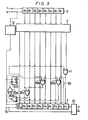
- Figure 7 schematically illustrates an example of an apparatus which carries out the conversion in accordance with this converting method.
- like parts corresponding to those in Figure 5 have the same references and will not be described in detail.
- the first bit of all the possible combinations is made variable so that a circuit for detecting whether the first bit is variable or fixed, namely, the circuit 5 as shown in Figure 5 which detects whether the combination is the combination having zero DC component (the first bit is fixed) or or the combination having the +2 DC components (the first bit is variable) or the like is not necessary.
- the output of the detecting circuit 8 which detects the DC component (DSV) is directly supplied to one input terminal of the EOR circuit 11.
- Other arrangements are formed similarly to Figure 5.
- the content or data of the shift register 7 is read out therefrom in response to the clock signal from the clock terminal 13, supplied through the EOR circuit 9 to the flip-flop circuit 10 and then developed at the output terminal 14 as the signal which is NRZI-coded.
- the detecting circuit 8 which detects the DC component becomes complicated in construction and becomes expensive in manufacturing cost.
- a digital signal into a non-return to zero, inverted-coded signal comprising the steps of:
- apparatus for converting a digital signal into a non-return to zero, inverted-coded signal comprising the steps of:
- this embodiment uses the identifying or detecting circuit 5 as used in the example shown in Figure 5.
- a T-type flip-flop circuit for example, is used as the flip- flop circuit 10.
- reference P o designates odd and/or even parity for P and Pe.
- the DC component is 0, while the detecting information Pe is 1, the DC component is ⁇ 2.
- P o P + Pe
- Pe represents the parity indicative of the number of "O”s
- P represents the parity indicative of "1”
- n in the m/n-conversion is taken as even number
- P may be the parity indicative of the number of "0"s. Accordingly, it is possible to say that P which is the odd and/or even parity of Pe and P is the parity indicative of the number of "0"s. That is, transmission information of the DC component is inverted, and then transmitted if the odd and/or even parity indicative of the number of "0"s at the odd-numbered bit of the combination is one.
- a detecting circuit 20 for detecting the DC component which comprises an EOR circuit 20a to which the first and third bits of ten bits of each combination are supplied, an EOR circuit 20b to which the fifth and seventh bits are supplied, an EOR circuit 20c to which the output from the EOR circuit 20b and the ninth bit are supplied, an ENOR circuit 20d to which the outputs from the EOR circuits 20a and 20c are supplied, and EOR circuit 20e which is supplied at one input terminal with the output from the ENOR circuit 20d, and a D-type flip-flop circuit 20f to which the output from the EOR circuit 20e is supplied.
- the output Q of the flip-flop circuit 20f is supplied to the other inputer terminal of the EOR circuit 20e, while the inverted output Q thereof is supplied to the other input terminal of the AND circuit 6.
- the EOR circuits 20a to 20c take the parities of the odd-numbered bits. In this case, since the number of odd-numbered bits is five if the number n is taken as ten, such parity is finally inverted by the ENOR circuit 20d as the parity indicative of the number of "0"s.
- the detecting circuit 20 produces the high level output when the DC component DSV' is -1.
- the identifying circuit 5 produces the high level output when the DC component is -2 so that the AND circuit 6 produces the signal "1" when the outputs of both the identifying circuit 5 and detecting circuit 20 are high level. Then, the output from the AND circuit 6 is supplied to one input terminal of the EOR circuit 11. At this time, the EOR circuit 11 inverts the first bit of the ten bits suppplied to the other input terminal thereof from the conversion logic circuit 3, and then supplies the first bit of the shift register 7.
- DSV' may be either 1 or -1 at the beginning of the modulation. Accordingly, as shown in Figures 5 and 7, the circuit which uses the AND circuits 8d and 8e and the NOR circuit 8f initially to set the DC component DSV to +1 or -1 is not required.
- FIG 9 schematically illustrates another embodiment of the present invention.
- the combination having zero DC component is used similarly to the combination having ⁇ 2 DC component in the state that all of the first bits are converted.
- the detecting circuit 5 which is used in Figure 8. Accordingly, in this case, only the detecting circuit for detecting the DC component is required, and hence the detecting signal circuit 20 used in Figure 8 is employed.
- the output of the detecting circuit 20, namely, the inverted output ⁇ of the flip-flop circuit 20f is directly supplied to one input terminal of the EOR circuit 11.
- this embodiment it is possible to achieve substantially similar action and effect to those of the first embodiment.
- this embodiment requires no identifying circuit 5 as compared with the first embodiment, so that the circuit arrangement can be simplified.
- the combination converted as mentioned above can be demodulated by a suitable demodulating circuit.
Abstract
Description
- This invention relates to digital data converting methods and apparatus. The methods and apparatus are suitable, for example, for use where an audio signal is pulse code modulated and then recorded.
- Apparatus is known in which an analog signal such as an audio signal is converted into a pulse code modulated (PCM) signal, magnetically recorded using a rotary head without forming guard-bands, and then reproduced. In such known apparatus, in addition to a differentiated output characteristic of the magnetic recording and a low frequency cross-talk component generated from adjacent tracks, low frequency components are cut off by a rotary transformer, so the low frequency components of the audio signal cannot be reproduced with high fidelity.
- Accordingly, in the above apparatus, which is required to have a narrow record and playback frequency band and a small low frequency component, it is effective to modulate a record signal into the area of the low frequency and direct current (DC) components by a modulating system having a small frequency spectrum component. The so-called non-return to zero, inverted (NRZI) modulation system is an example of such a modulation system. In the NRZI system, a signal is inverted at level "1" in the data signal, but is not inverted at level "0" therein.
- However, in the NRZI modulation system, when consecutive digital zeroes appear, the modulated signal is not inverted during the period occupied by the digital zeroes, and the frequency of the modulated signal becomes low. Thus, the DC and the low frequency components are increased.
- Therefore, it has been proposed to divide the PCM digital information into groups of bits of a predetermined number and to convert the respective groups of bits into groups of a large number, thereby avoiding the occurrence of a large number of consecutive digital zeroes.
- We have previously proposed such an information converting system as follows.
- In this converting system, eight bits (B1, B2, B3, B4, B5, B6, B7, Bs) of digital information in a base digital signal are converted to ten bits (P1, P2, P3, P4, P5, Ps, P7, Ps, Pg, P10). Eight bits (B1, B2, B3, B4, Bs, Bs, B7, B8) can be combined in 256(2S) different ways.
- With ten bits (P1, P2, P3, P4, P5, Ps, P7, Ps, Pg, Pio), in order to avoid a DC component (or charge) in the signal after the NRZI modulation, it is sufficient that five bits in ten bits are positive "1" and five bits are negative "0". In order to establish Tmax/Tmin = 4 (where Tmax is the maximum internal between levelal :ransistions and Tmin is the minimum interval between level transitions), a condition is required such that in n the NRZI-coding, the number of consecutive digital zeroes is less than three, or in the converted signal the number of consecutive bits of the same level is less than four.
- With the above constraints, the following Table I shows the possible combinations of ten digital bits in the NRZI code for which the DC component is zero, but in which there are no more than three digital zeroes in a row (either internally of each 10-bit word or at the boundary between two such words):

- Table I shows that there are numerous possible combinations that will satisfy the constraints. For example, if up to three digital zeroes are permitted at the beginning of each word, then no digital zeroes can be permitted at the end of any word. In that case, Table I shows the total of the possible combinations is:

- From all of the combinations in Table I, the maximum total is achieved if no more than two digital zeroes are permitted at the beginning of a 10-bit converted word and no more than one digital zero is permitted at the end. In that case, the total is:

- Since there are 256 possible 8-bit words of original data, 63 additional 10-bit combinations are required to represent all of the original data. Thus, it is necessary to use 10-bit combinations for which the DC component is not zero.
- The following table illustrates the number of possible 10-bit combinations, which begin with no more than two digital zeroes and end with no more than one digital zero, having a DC component of 0, -2 and +2 when NRZI-coded.

- From Table II, it is clear that the number of possible combinations in which the DC component is -2 is:


- To calculate the DC components for Table 11, it was assumed that the last bit of the next-preceding 10- bit combination was at the low level "0", as shown in Figures 1A to 1C of the accompanying drawings. If Table II were constructed by assuming that the level of the last bit of the preceding word was high "1", then "-2" and "2" columns would be interchanged as shown in Figures 2A and 2B.
- Further, the low frequency spectrum of the modulation wave tends to decrease more if the combination alternately using the combination with +2 and -2 DC component is used more frequently than the combinations with a zero DC component. Accordingly, 125 combinations with a pair of +2 and -2 DC components are used and the remaining 131 combinations with a zero DC component are used for 256 combinations of eight bit, by which 125 combinations and 131 combinations are made corresponding respectively to 256 combinations of eight bits.
- As the combinations with the pair of +2 and -2 DC components, the pair may be selected such that DC component can be controlled only by changing the first bit (the second bit and the following bits in combinations of a pair are formed as the same level). Therefore, of the possible combinations in, for example, Table II, the combinations with +2 and -2 DC components and the first bit beginning with "0":

- That is, as shown in Figures 3A and 3B of the accompanying drawings, when the combinations with ±2 DC components appears, the number of level transistions P (the number of digital ones) from the second bit is counted, in which until the following combination with ±2 DC components appears, if the number of level transitions is even, the first bit (shown by an inverted delta) is converted to digital one as shown in Figure 3A, while if the number of level transitions is odd, the first bit remains as digital zero as shown in Figure 3B.
- Thus, even if ±2 DC components appear, they are cancelled out by ±2 DC components of the succeeding combination and hence regardless of any consecutive digital components, the DC component becomes zero.
- The DC component of each bit is generally called a digital sum variation (DSV), which is one of the evaluation methods. Let it be considered that a combination is formed of a 10-bit pattern with zero DC component as, for example, shown in Figure 4A of the accompanying drawings. When transition of DSV begins with DSV = 1, the change of the DSV of such a combination is as shown by a solid line in Figure 4B of the accompanying drawings.
- If the width between the maximum and minimum values of the DSV is small, the DSV has a small DC component and the low frequency component is reduced. As one of the evaluation methods, there is further known a parameter which is generally referred to as DSV variance. The DSV variance can be obtained by squaring and averaging the DSV values at every bit, and it is desired that the DSV variance is as small as possible. While the level of DSV = 0 is defined as an average value of the DSV value of every bit, the level of DSV regarding the waveform of the combination (code) which has been NRZI-coded is defined as DSV max = -DSV min. Accordingly, in this case, it is convenient that the DSV at the boundary between the respective combinations is taken as +1 or -1 and the intermediate value between DSV max and DSV min is defined as DSV = 0.
- Therefore, let us consider the above converting method by using the evaluation method of DSV variance. In the combination as, for example, shown in Fiugre 4A, when the evaluation of DSV variance begins with DSV = +1, the transistion of DSV changes along the solid line shown in Figure 4B as described above and the DSV variance at that time becomes 1.7. While, when the evaluation of the DSV variance begins with DSV = -1, the transition of DSV changes as shown by a broken line in Figure 4B, and the DSV variance at that time becomes 6.9. That is, combinations of the same bit pattern are made to have different DC characteristics depending on the initial setting of DSV. Particularly in this case, when the evaluation of DSV variance begins with DSV = -1, the DSV variance becomes large, which is not preferable.
- Figure 5 of the accompanying drawings shows an example of an apparatus which is capable of conversion in accordance with the above converting system. The apparatus comprises an
input terminal 1, an 8-bit shift register 2 which accepts information of eight bits, aconversion logic circuit 3 which uses, for example, a programmable logic array (PLA), and aclock terminal 4. Then, information applied to theinput terminal 1 is transferred eight bits at a time through theshift register 2 in response to a pulse which is applied to theclock terminal 4 at the data bit rate, and the information of eight bits (Bi, B2, B3, B4, B5, Bo, B7, Bs) is supplied to theconversion logic circuit 3. - An identifying
circuit 5 identifies whether the first bit is variable or fixed, namely, in this case, whether the DC component of the combination is "0" or +2. The identifyingcircuit 5 consists of, for example, exclusive-OR (hereinafter simply referred to as EOR)circuits 5a to 5c and an exclusive-NOR (hereinafter simply referred to as ENOR)circuit 5d. In the identifyingcircuit 5, thecircuits 5a to 5d carry out modulo addition of the even-numbered bits of the output from theconversion logic circuit 3. In other words, the identifyingcircuit 5 detects whether the number of digital zeroes of the even-numbered bits is even or odd. If it is 0 (even), the identifyingcircuit 5 identifies that the combination has ±2 DC components and produces high level "1" at its output side, namely, the output side of theENOR circuit 5d. That is, the identifyingcircuit 5 carries out all EOR logic operations of the even-numbered bit outputs of the output of theconversion logic circuit 3. In this case, when the even-numbered bit is "1", the level transition is carried out in this portion so that the DC components of this bit and the immediately preceding bit become 0. While, when the even-numbered bit is "0", there exist ±2 DC components. Further, when there are two digital zeroes, the DC component becomes 0 to ±4. In like manner, when there are three digital zeroes, the DC component be becomes ±2 or ±6. In other words, if the number of digital zeroes is even, the DC component becomes 0, ±4, ±8,.... while if it is odd, the DC component becomes ±2, ±6, ±10,..... On the other hand, the whole of the DC component of ten bits is restricted to 0 or -2. Accordingly, by detecting whether the number of digital zeroes of the above even-numbered bit is even or odd, it is possible to identify whether the DC component is 0 or ±2. - The output of the identifying
circuit 5 is supplied to one input terminal of an ANDcircuit 6, and the ANDcircuit 6 is supplied at its other input terminal with an output from a detectingcircuit 8 which is provided at the output side of theshift register 7 for detecting the DC component (DSV) of each combination. The detectingcircuit 8 supplied the high level output to the input side of the ANDcircuit 6 when the DC component DSV' up to the preceding combination is, for example, -1. - The output of the AND
circuit 6 is supplied to one input terminal of anEOR circuit 11 which inverts the first bit level. To the other input terminal of theEOR circuit 11 is supplied the first bit P1 of ten bits from theconversion logic circuit 3. Accordingly, when the output of the ANDcircuit 6 if "0", the first bit P1 is not inverted in level and fed as it is to theshift register 7, while even when the output of the ANDcircuit 6 is "1", the first bit P1 is inverted in polarity and fed to theshift register 7. - Further, in Figure 5, an
EOR circuit 9 and a D-type flip-flop circuit 10 constitute an NRZI-modulating circuit. - The detecting
circuit 8 includes an up-down counter 8a, and thecounter 8a is driven by a clock frequency to count only the even-numbered bits. Further, the up-down counter 8a is controlled by the output from theEOR circuit 9, so the DC component is detected. Since the output of the up-down counter 8a is always delayed by two bits, theEOR circuits counter 8a by the last two bits. - In the detecting
circuit 8, ANDcircuits circuit 8f are used initially to set the DC component DSV to -1 or +1. When the DSV of the NRZI-modulated wave is counted by thecounter 8a at every one or two bits, if the state of the DSV is taken as DSV is less than or equal to 3 in the range of DSV, there exist many DC components such as -3, -2, -1,0, +1, +2 and +3. Accordingly, the DSV is initially set to -1 or +1 by the ANDcircuits circuit 8f. - Thus, the positive or negative polarity of the DC component is detected, and this detected signal and the signal from the identifying
circuit 5 are supplied to the ANDcircuit 6 which then produces a control signal for controlling the level of the first bit of the output. - As to the combination of DC component in which it is a combination with zero DC component and a combination with ±2 DC components, the
conversion logic circuit 3 is arranged to produce it to be any one of them as unified. When theconversion logic circuit 3 produces the output which is unified such that the DC component is -2, if the converted combination has -2 DC component and the evaluation of DSV' variance with -1, the first bit thereof is inverted by the EOR circuit 11 (at this time, the output of the ANDcircuit 6 is high level) and a combination having +2 DC component is then produced. Since the output of the identifyingcircuit 5 is low level and the output of the ANDcircuit 6 is also low level for the combination with a zero DC component, it is directly produced without the first bit being inverted in level by theEOR circuit 11. - A
timing detector circuit 12 detects the timing of the pulse which is supplied to theclock terminal 4 at the data bit rate, and the timing signal from thetiming detector circuit 12 is supplied to a load terminal LD of theshift register 7 at every 8-bit data. - As described above, the content or data converted to the form of 10-bit data and latched in the
shift register 7 is sequentially read out therefrom on the basis of a clock signal withfrequency 5/4 times the clock frequency of the input signal supplied thereto from aclock terminal 13. The signal thus read out from theshift register 7 is supplied to and NRZI-coded by the NRZI-modulating circuit which comprises theEOR circuit 9 and the flip-flop circuit 10, and is then fed to anoutput terminal 14. - In the case of the circuit arrangement in which PLA is used for the
conversion logic circuit 3 as described above, the circuit for detecting whether the combination has zero DC component of +2 DC component is required so that the circuit arrangement becomes complicated. This poses no problem when a read-only memory (ROM) is used as theconversion logic circuit 3. However, the ROM causes the circuit arrangement to become large, and when this ROM is formed in an integrated circuit, the ROM occupies a large pattern area and consumes much power. Further, in order to make the DSV variance small, it is desired that two combinations having zero DC component are paired as much as possible, and that one of the pair having a smaller DSV variance is used on the basis of whether the DSV is +1 or -1. In this case, a detecting circuit is required to detect whether or not the first bit of the pair of the two combinations having the equal zero DC component is variable. This makes the circuit arrangement more complicated. - Further, if a pair of two combinations are not limited to ones in which bits succeeding the second bit are equal, but are selected from one having a small DSV variance, although the DSV variance can be made smaller, it is unavoidable that the circuit arrangement becomes more and more complicated.
- Further, if a pair of two combinations are not limited to one in which bits succeeding the second bit are equal, but are selected from ones having a small DSV variance, although the DSV variance can be made smaller, it is unavoidable that the circuit arrangement becomes more and more complicated.
- Therefore, a converting system has been considered which uses no detecting circuit.
- In this converting system, when the combination in which DC component is zero is used, all the first bits thereof are converted similarly to the combination in which the DC component is ±2. To this end, even when the first bit is inverted, possible combination must be formed in 2 x2m different ways, or the 8/10- conversion scheme must have 2 x 256 possible combinations. It is therefore assumed that Tma, = 5T' (T' = Tmin = Tw (window margin of detecting window)). Then, the number of the usable combinations is 512 or above.
- The following Table III shows the number of possible combinations of 10-bit iformation which can satisfy the condition of T max = 5T'. In this case, to satisfy the condition of T max = 5T', in NRZI code, the number of consecutive digital zeroes must never exceed four, or the same consecutive levels of digital signal after being modulated must never exceed five bits. Therefore, the bits must begin with at most two digital zeroes and also end with at most two digital zeroes.

- In Table lll, the information or word beginning with "100... ", if the first bit thereof is inverted, becomes "000...", so that three consecutive digital zeroes are permitted at the beginning thereof. There is then a risk that four or more consecutive digital zeroes will occur at the boundary between the consecutive combinations, thus such combinations cannot be used in this converting method. As a result, if these 55 (3 + 18 +34) combinations are removed from all the possible combinations in Table III, 512 combinations are left, which is just twice the number of possible combinations of 28 = 256.
- Accordingly, 256 possible combinations each of which forms a pair with a different first bit can be made corresponding to 256 possible combinations of 8-bit data. In this connection, Table III shows 102 possible combinations each of which forms a pair having a zero DC component and has a different first bit, and 154 possible combinations each of which forms a pair having ±2 DC components and has a different first bit.
- Upon conversion, the pair of combinations are selected by detecting which of DSV = +1 or -1 make the DSV variance small. As described above in connection with Figure 4, when the DC component is -2, the evaluation of DSV variance begins with DSV = +1, while the DC component is +2, the evaluation of DSV variance begins with DSV = -1.
- Figure 6 of the accompanying drawings (formed of Figures 6A to 6E) shows examples of 356 possible combinations (codes) which are selected on the basis of Table III, in which they are not corresponded to the data. Figure 6 shows that a pair of two combinations should be selected only by controlling, for example, the first bit. In Figure 6, reference Q' designates the DC component information (corresponding to the preceding DSV = DSV') of the code (combination) before being converted, DV designated the variance of DSV, P designates the number of level transitions (even number is 0 and odd number is 1) in each code, and Q designates the DC component information (corresponding to the DSV of the code just after being converted) of the code just after being converted. When the example of the circuit arrangement shown in Figure 5 uses the code of combinations in Figure 6, a pair of codes from
numbers 1 to 102 having zero DC component are used individually. - Figure 7 schematically illustrates an example of an apparatus which carries out the conversion in accordance with this converting method. In Figure 7, like parts corresponding to those in Figure 5 have the same references and will not be described in detail.
- In the example shown in Figure 7, upon conversion, the first bit of all the possible combinations is made variable so that a circuit for detecting whether the first bit is variable or fixed, namely, the
circuit 5 as shown in Figure 5 which detects whether the combination is the combination having zero DC component (the first bit is fixed) or or the combination having the +2 DC components (the first bit is variable) or the like is not necessary. - Therefore, in this example, the output of the detecting
circuit 8 which detects the DC component (DSV) is directly supplied to one input terminal of theEOR circuit 11. Other arrangements are formed similarly to Figure 5. - The
conversion logic circuit 3 produces its output with the first bit unified such that the preceding DSV' becomes -1 or +1. Accordingly, let it be assumed that DSV' = +1 be unified for the first bit. Then, when the converted combination begins with DSV' = -1, it is sufficient that the high level output of the detectingcircuit 8 is supplied to theERO circuit 11, in which the first bit thereof is inverted in level and then supplied to theshift register 7. - Accordingly, similarly to the above, the content or data of the
shift register 7 is read out therefrom in response to the clock signal from theclock terminal 13, supplied through theEOR circuit 9 to the flip-flop circuit 10 and then developed at theoutput terminal 14 as the signal which is NRZI-coded. - As mentioned above, without using the detecting circuit 5 (and the AND circuit 6) as shown in Figure 5, it is possible to carry out the eight to ten conversion.
- However, in the case of the prior circuit as mentioned above, since the waveform NRZI-coded in each combination is used to count the DC component, the detecting
circuit 8 which detects the DC component becomes complicated in construction and becomes expensive in manufacturing cost. - The methods and apparatus as discussed above are generally as disclosed in our European patent specification EP-A1-0 143 553 (EPC Article 54(3)).
- According to the present invention there is provided a method of converting a digital signal into a non-return to zero, inverted-coded signal, the method comprising the steps of:
- a) dividing a basic digital signal into a series of basic words, each word having m bits of data;
- b) converting said basic words into converted words, each of said converted words having n bits of data, wherein n is greater than m + 1, the series of converted words comprising a predetermined maximum number of consecutive digital zeroes;
- c) said converted words comprising primary combinations of n bits having a DC component equal to zero when NRZI-coded, and pairs of secondary combinations of n bits having a DC component with a magnitude of two when NRZI-coded, the DC component of the combinations of each being of opposite polarity, and the pairs being chosen to differ only in the first bit of data thereof;
- d) generating a control signal in response to the digital sum variation in the series of converted words preceding the respective word to be converted in response to the detection of a primary or a secondary combination, by forming a first signal indicating if the number of digital zeroes in the respective word to be converted is even, and comparing said first signal with the preceding control signal for generating the respective control signal;
- e) selectively inverting the first bit of data of a secondary combination in response to said control signal; and
- f) generating from said converted words said NRZI-coded signal.
- According to the present invention there is also provided a method of converting a digital signal into a non-return to zero, inverted-coded signal, the method comparing the steps of:
- a) dividing a basic digital signal into a series of basic words, each word having m bits of data;
- b) converting said basic words into converted words, each of said converted words having n bits of data, wherein n is greater than m + 1, the series of converted words comprising a predetermined maximum number of consecutive digital zeroes;
- c) said converted words comprising primary pairs of combinations of n bits having a DC component equal to zero when NRZI-coded, and pairs of secondary combinations of n bits having a DC component with a magnitude of two when NRZI-coded, the DC component of the combinations of each being of opposite polarity, and the primary and secondary combinations of each pair being chosen to differ only in the first bit of data thereof;
- d) generating a control signal in response to the digital sum variation in the series of converted words preceding the respective word to be converted, by forming a first signal indicating if the number of digital zeroes in the respective word to be converted is even, and comparing said first signal with the preceding control signal for generating the respective control signal;
- e) selectively inverting the first bit of data of a secondary combination in response to said control signal; and
- f) generating from said converted words said NRZI-coded signal.
- According to the present invention there is also provided apparatus for converting a digital signal into a non-return to zero, inverted-coded signal, the method comprising the steps of:
- a) means for dividing a basic digital signal into a series of basic words, each word having m bits of data;
- b) means for converting said basic words into converted words, each of said converted words having n bits of data, wherein n is greater than m + 1, the series of converted words comprising a predetermined maximum number of consecutive digital zeroes;
- c) said converted words comprising primary combinations of n bits having a DC component equal to zero when NRZI-coded, and pairs of secondary combinations of n bits having a DC component with a magnitude of two when NRZI-coded, the DC component of the combinations of each being of opposite polarity, and pairs being chosen to differ only in the first bit of data thereof;
- d) means for generating a control signal in response to the digital sum variation in the series of converted words preceding the respective word to be converted and in response to the detection of ai primary or a secondary combination, by forming a first signal indicating if the number of digital zeroes in the respective word to be converted is even, and comparing said first signal with the preceding control signal for generating the respective control signal;
- e) means for selectively inverting the first bit of data of a secondary combination in response to said control signal; and
- f) means for generating from said converted words said NRZI-coded signal.
- According to the present invention there is also provided apparatus for converting a digital signal into a non-return to zero, inverted-coded signal, the method comparing the steps of:
- a) means for dividing a basic digital signal into a series of basic words, each word having m bits of data;
- b) means for converting said basic words into converted words, each of said converted words having n bits of data, wherein n is greater than m + 1, the series of converted words comprising a predetermined maximum number of consecutive digital zeroes;
- c) said converted words comprising primary pairs of combinations of n bits having a DC component equal to zero when NRZI-coded, and pairs of secondary combinations of n bits having a DC component with a magnitude of two when NRZI-coded, the DC component of the combinations of each being of opposite polarity, and the primary and secondary combinations of each pair being chosen to differ only in the first bit of data thereof;
- d) means for generating a control signal in response to the digital sum variation in the series of converted words preceding the respective word to be converted, by forming a first signal indicating if the number of digital zeroes in the respective word to be converted is even, and comparing said first signal with the preceding control signal for generating the respective control signal;
- e) means for selectively inverting the first bit of data of a secondary combination in response to said control signal; and
- f) means for generating from said converted words said NRZI-coded signal.
- The invention will now be described by way of example with reference to the accompanying drawings, throughout which like parts are referred to by like references, and in which:
- Figures 1Ato 1 C respectively illustrate possible 10-bit combinations of an NRZI-coded converted digital signal;
- Figure 2A illustrates a 10-bit combination of an NRZI-coded converted digital signal;
- Figure 2B illustrates the 10-bit combination shown in Figure 2A with the first bit thereof inverted from a digital zero to a digital one;
- Figures 3A and 3B respectively illustrate converted digital signals;
- Figures 4A and 4B respectively illustrate a converted digital signal and variation of the DSV of the converted digital signal;
- Figure 5 schematically illustrates an apparatus for generating an n-bit NRZI-coded converted digital signal from an m-bit base digital signal;
- Figure 6 (formed of Figures 6A to 6E) is a diagram showing different 10-bit patterns;
- Figure 7 schematically illustrates an apparatus for generating an n-bit NRZI-coded converted digital signal from an m-bit base digital signal;
- Figure 8 schematically illustrates an embodiment of information converting apparatus according to the present invention; and
- Figure 9 schematically illustrates another embodiment of information converting apparatus according to the present invention.
- The embodiment of Figure 8 comprises a circuit arrangement corresponding to the example of the conversion for T max = 4T' which is based on Table II, namely, the example of the circuit shown in Figure 5. Accordingly, in Figure 8, like parts corresponding to those in Figure 5 are marked with the same references and will not be described in detail.
- As described above, in the case of T max = 4T', there exist combinations having zero DC component (or charge) (the first bit is fixed) and ±2 DC components (the first bit is variable) so that they must be discriminated from each other. Accordingly, this embodiment uses the identifying or detecting
circuit 5 as used in the example shown in Figure 5. In this case, a T-type flip-flop circuit, for example, is used as the flip-flop circuit 10. - For this embodiment, an explanation will be given for a case in which the DC component of a present combination for the succeeding combination can be calculated only by checking the parity of odd and/or even of an odd-numbered bit of the combination, without using the NRZI-coded waveform.
- As described above, to detect whether the DC component of the combination is 0 or ±2, the even-numbered bit of the combination is taken into consideration. Then, if the number of digital zeroes is even, the DC component is 0 (DC = 0), while if it is odd, the DC component is regarded as ±2 (DC = ±2). In this case, let it be assumed that the detection information is Pe. And so, if Pe = 0, then the DC component is 0, while if Pe = 1, the DC components is ±2. Then, if the
conversion logic circuit 3 produces its output of combination having the DC component DSV' = ±1 up to that time, when Pe = 1, the combination may be restricted as that with the -2 DC component. Accordingly, when Pe = 1 and DSV = -1, the first bit of the combination is inverted in level to be the combination having 2 DC component. - Next, from the combination of n bits which were inverted in level as required, namely, 10-bit combinations in this case, the DC component is calculated for the succeeding combination. Let us assume that the parity of odd and/or even of the n-bit combination is P. Then, for zero DC component, if P = 0, DSV = DSV' is established, while if P = 1, DSV = -DSV' is established. On the other hand, for the DC component of ±2, if P = 0, DSV = -DSV', while if P = 1, DSV = DSV'. The reason for this is as follows. -When the DC component is 0, the DSV is not changed, so that DSV = DSV' is established. However, since the last bit of the NRZI-coded waveform in the waveform in the combination of P = 1 is the opposite level to the last bit of the preceding combination, if the DSV is defined assuming that the level of the last bit of the preceding combination is low level, that last bit of the present combination is high level, so that such level becomes the low level for the succeeding combination. In consequence, it is necessary to invert the code of the DC component information.
- For the DC component of ±2, if P = 0, the state of the DC component is changed and the range in which the DC component is changed is limited from +1 to -1 or -1 to +1 so that DSV = -DSV' is finally established. On the other hand, when P = 1 is established, the level of the last bit is different from the level of the last bit of the preceding combination so that DSV = DSV' is finally established.
- To summarize the above facts, only when the DC component is 0 and P = 1 and the DC component is ±2 and P = 0, it is sufficient for the DC component information that the DC component information of the preceding combination is inverted. The following Table IV shows the above in summarized form.

- In Table IV, reference Po designates odd and/or even parity for P and Pe. When the detecting information Pe is 0, the DC component is 0, while the detecting information Pe is 1, the DC component is ±2. Thus, under the condition that the modulo addition of P and Pe is expressed as Po (Po = P + Pe), when Po is 1, the level of the DC component DSV is inverted.
- Further, Pe represents the parity indicative of the number of "O"s, although P represents the parity indicative of "1", if n in the m/n-conversion is taken as even number, P may be the parity indicative of the number of "0"s. Accordingly, it is possible to say that P which is the odd and/or even parity of Pe and P is the parity indicative of the number of "0"s. That is, transmission information of the DC component is inverted, and then transmitted if the odd and/or even parity indicative of the number of "0"s at the odd-numbered bit of the combination is one.
- Therefore, in this embodiment, there is provided a detecting
circuit 20 for detecting the DC component, which comprises an EOR circuit 20a to which the first and third bits of ten bits of each combination are supplied, anEOR circuit 20b to which the fifth and seventh bits are supplied, anEOR circuit 20c to which the output from theEOR circuit 20b and the ninth bit are supplied, anENOR circuit 20d to which the outputs from theEOR circuits 20a and 20c are supplied, andEOR circuit 20e which is supplied at one input terminal with the output from theENOR circuit 20d, and a D-type flip-flop circuit 20f to which the output from theEOR circuit 20e is supplied. The output Q of the flip-flop circuit 20f is supplied to the other inputer terminal of theEOR circuit 20e, while the inverted output Q thereof is supplied to the other input terminal of the ANDcircuit 6. - The EOR circuits 20a to 20c take the parities of the odd-numbered bits. In this case, since the number of odd-numbered bits is five if the number n is taken as ten, such parity is finally inverted by the
ENOR circuit 20d as the parity indicative of the number of "0"s. When its value is 1, the output of the flip-flop circuit 20f is inverted by theEOR circuit 20e at the next stage. In other words, the preceding DC component information is inverted in level and then supplied to the flip-flop circuit 20f. Then, in order that when DSV' = -1, namely, the signal level is "0", the signal level "1" is supplied, the inverted outputQ is derived from the flip-flop circuit 20f and then fed to the other input terminal of the ANDcircuit 6. - Consequently, the detecting
circuit 20 produces the high level output when the DC component DSV' is -1. - On the other hand, as mentioned above, the identifying
circuit 5 produces the high level output when the DC component is -2 so that the ANDcircuit 6 produces the signal "1" when the outputs of both the identifyingcircuit 5 and detectingcircuit 20 are high level. Then, the output from the ANDcircuit 6 is supplied to one input terminal of theEOR circuit 11. At this time, theEOR circuit 11 inverts the first bit of the ten bits suppplied to the other input terminal thereof from theconversion logic circuit 3, and then supplies the first bit of theshift register 7. - As set forth above, in this embodiment, without using the NRZI-coded waveform, merely by checking the odd and/or even parity of the odd-numbered bits of each combination, it is possible to calculate the DC component for the succeeding combination so that the circuit arrangement can be simplified.
- Since there exist two states of -1 DC component and +1 DC component ("0" and "1" in signal level), DSV' may be either 1 or -1 at the beginning of the modulation. Accordingly, as shown in Figures 5 and 7, the circuit which uses the AND
circuits circuit 8f initially to set the DC component DSV to +1 or -1 is not required. - Figure 9 schematically illustrates another embodiment of the present invention. This embodiment corresponds to the example of the conversion of T max = 5T' based on Table III, namely, the example of the circuit shown in Figure 7. Accordingly, in Figure 9, like parts corresponding to those in Figure 7 are marked with the same reference and will not be described in details.
- As described above, in the case of Tmax = 5T', the combination having zero DC component is used similarly to the combination having ±2 DC component in the state that all of the first bits are converted. As a result, it is not necessary to use the detecting
circuit 5 which is used in Figure 8. Accordingly, in this case, only the detecting circuit for detecting the DC component is required, and hence the detectingsignal circuit 20 used in Figure 8 is employed. In that case, the output of the detectingcircuit 20, namely, the inverted output Ö of the flip-flop circuit 20f is directly supplied to one input terminal of theEOR circuit 11. - Also in this case, if the output from the
logic conversion circuit 3 is produced unified in the combination having, for example, DSV = +1, when the converted combination begins with DSV = 1, the high level output is supplied from the detectingcircuit 20 to theEOR circuit 11, in which the first bit thereof is inverted and then fed to theshift register 7. - As described above, according to this embodiment, it is possible to achieve substantially similar action and effect to those of the first embodiment. In particular, this embodiment requires no identifying
circuit 5 as compared with the first embodiment, so that the circuit arrangement can be simplified. - In embodiments of this invention, the combination converted as mentioned above can be demodulated by a suitable demodulating circuit.
- While in the above embodiments the case of T max = 4T' and Tmax = 5T' are described, the invention is not limited to the above cases, but can be applied to other combinations including a combination in which at least the DC component is controlled to be less than ±2, for example, a combination which can be controlled to be combined with a combination having zero DC component and whose DC component is fixed.
Claims (10)
Priority Applications (1)
| Application Number | Priority Date | Filing Date | Title |
|---|---|---|---|
| AT84308148T ATE58270T1 (en) | 1983-11-24 | 1984-11-23 | PROCEDURE AND ARRANGEMENT FOR DIGITAL DATA CONVERSION. |
Applications Claiming Priority (2)
| Application Number | Priority Date | Filing Date | Title |
|---|---|---|---|
| JP58221235A JPS60113366A (en) | 1983-11-24 | 1983-11-24 | Information conversion system |
| JP221235/83 | 1983-11-24 |
Publications (3)
| Publication Number | Publication Date |
|---|---|
| EP0143005A2 EP0143005A2 (en) | 1985-05-29 |
| EP0143005A3 EP0143005A3 (en) | 1987-04-01 |
| EP0143005B1 true EP0143005B1 (en) | 1990-11-07 |
Family
ID=16763583
Family Applications (1)
| Application Number | Title | Priority Date | Filing Date |
|---|---|---|---|
| EP84308148A Expired - Lifetime EP0143005B1 (en) | 1983-11-24 | 1984-11-23 | Digital data converting methods and apparatus |
Country Status (9)
| Country | Link |
|---|---|
| US (1) | US4577180A (en) |
| EP (1) | EP0143005B1 (en) |
| JP (1) | JPS60113366A (en) |
| KR (1) | KR930005644B1 (en) |
| AT (1) | ATE58270T1 (en) |
| AU (1) | AU564002B2 (en) |
| CA (1) | CA1227871A (en) |
| DE (1) | DE3483562D1 (en) |
| ES (1) | ES8607648A1 (en) |
Families Citing this family (16)
| Publication number | Priority date | Publication date | Assignee | Title |
|---|---|---|---|---|
| US4833471A (en) * | 1984-03-26 | 1989-05-23 | Canon Kabushiki Kaisha | Data processing apparatus |
| US4775985A (en) * | 1987-04-06 | 1988-10-04 | Sony Corporation | Method of dc-free 8/9 nrz coding using a unique sync word pattern |
| JP2508491B2 (en) * | 1987-09-28 | 1996-06-19 | ソニー株式会社 | Data playback device |
| US4967289A (en) * | 1987-09-30 | 1990-10-30 | Sony Corporation | PCM signal recording apparatus |
| JPH01107373A (en) * | 1987-10-21 | 1989-04-25 | Sony Corp | Data reproducing device |
| GB8912471D0 (en) * | 1989-05-31 | 1989-07-19 | Int Computers Ltd | Data transmission code |
| JPH0362621A (en) * | 1989-07-31 | 1991-03-18 | Ricoh Co Ltd | Data modulation system |
| EP0416930B1 (en) * | 1989-09-08 | 1997-11-12 | Fujitsu Limited | Encoding and decoding circuit for run-length-limited coding |
| DE4011894A1 (en) * | 1990-04-12 | 1991-10-17 | Thomson Brandt Gmbh | TRANSMISSION PROCESS FOR A BINARY SIGNAL |
| EP0593173B1 (en) * | 1992-10-16 | 1998-11-11 | Matsushita Electric Industrial Co., Ltd. | Apparatus for recording digital signals by controlling frequency characteristics of digital signals |
| JP3528929B2 (en) * | 1993-09-22 | 2004-05-24 | ソニー株式会社 | Magnetic recording device |
| PL342427A1 (en) * | 1998-12-21 | 2001-06-04 | Koninkl Philips Electronics Nv | Apparatus for encoding n-bit source words into corresponding m-bit channel words and decoding m-bit channel words into corresponding n-bit source ones |
| US6492918B1 (en) * | 1999-09-30 | 2002-12-10 | Stmicroelectronics, Inc. | Code word having data bits and code bits and method for encoding data |
| DE102006056903B4 (en) * | 2006-12-02 | 2008-07-17 | Semikron Elektronik Gmbh & Co. Kg | Method for digital communication between two functional blocks of a power electronic component |
| JP6197249B2 (en) * | 2014-07-30 | 2017-09-20 | 日立建機株式会社 | Power transmission device for vehicle |
| CN104682922A (en) * | 2014-12-02 | 2015-06-03 | 国家电网公司 | High-speed RZ/NRZ conversion device and NRZ/RZ conversion device |
Citations (1)
| Publication number | Priority date | Publication date | Assignee | Title |
|---|---|---|---|---|
| EP0143553A1 (en) * | 1983-10-27 | 1985-06-05 | Sony Corporation | Methods of and apparatus for digital data conversion |
Family Cites Families (8)
| Publication number | Priority date | Publication date | Assignee | Title |
|---|---|---|---|---|
| GB1250908A (en) * | 1968-12-13 | 1971-10-27 | ||
| US4001811A (en) * | 1972-01-28 | 1977-01-04 | General Motors Corporation | Method and apparatus for coding and decoding digital information |
| NL7707540A (en) * | 1977-07-07 | 1979-01-09 | Philips Nv | DEVICE FOR CODING SIGNALS DISTRIBUTED OVER A NUMBER OF CHANNELS. |
| JPS5619506A (en) * | 1979-07-23 | 1981-02-24 | Sony Corp | Code converting method |
| JPS5665311A (en) * | 1979-10-27 | 1981-06-03 | Nippon Telegr & Teleph Corp <Ntt> | Magnetic recording and reproduction system for digital information |
| US4352129A (en) * | 1980-02-01 | 1982-09-28 | Independent Broadcasting Authority | Digital recording apparatus |
| NL186790C (en) * | 1980-07-14 | 1991-02-18 | Philips Nv | METHOD FOR CODING A SERIES OF BLOCKS OF BILINGUAL DATA BITS IN A SERIES OF BLOCKS OF DUAL CHANNEL BITS, AND USING MODULATOR, DEMODULATOR AND RECORD CARRIER IN THE METHOD |
| JPS57195308A (en) * | 1981-05-26 | 1982-12-01 | Sony Corp | Block coding method |
-
1983
- 1983-11-24 JP JP58221235A patent/JPS60113366A/en active Granted
-
1984
- 1984-11-20 CA CA000468199A patent/CA1227871A/en not_active Expired
- 1984-11-20 US US06/673,374 patent/US4577180A/en not_active Expired - Lifetime
- 1984-11-23 KR KR1019840007359A patent/KR930005644B1/en not_active IP Right Cessation
- 1984-11-23 AU AU35831/84A patent/AU564002B2/en not_active Expired
- 1984-11-23 EP EP84308148A patent/EP0143005B1/en not_active Expired - Lifetime
- 1984-11-23 AT AT84308148T patent/ATE58270T1/en not_active IP Right Cessation
- 1984-11-23 DE DE8484308148T patent/DE3483562D1/en not_active Expired - Lifetime
- 1984-11-23 ES ES537900A patent/ES8607648A1/en not_active Expired
Patent Citations (1)
| Publication number | Priority date | Publication date | Assignee | Title |
|---|---|---|---|---|
| EP0143553A1 (en) * | 1983-10-27 | 1985-06-05 | Sony Corporation | Methods of and apparatus for digital data conversion |
Also Published As
| Publication number | Publication date |
|---|---|
| CA1227871A (en) | 1987-10-06 |
| KR930005644B1 (en) | 1993-06-23 |
| ES537900A0 (en) | 1986-05-16 |
| ATE58270T1 (en) | 1990-11-15 |
| KR850005061A (en) | 1985-08-19 |
| JPS60113366A (en) | 1985-06-19 |
| AU564002B2 (en) | 1987-07-30 |
| AU3583184A (en) | 1985-05-30 |
| EP0143005A3 (en) | 1987-04-01 |
| EP0143005A2 (en) | 1985-05-29 |
| US4577180A (en) | 1986-03-18 |
| JPH0519226B2 (en) | 1993-03-16 |
| ES8607648A1 (en) | 1986-05-16 |
| DE3483562D1 (en) | 1990-12-13 |
Similar Documents
| Publication | Publication Date | Title |
|---|---|---|
| EP0143553B1 (en) | Methods of and apparatus for digital data conversion | |
| EP0143005B1 (en) | Digital data converting methods and apparatus | |
| KR100263689B1 (en) | Modulating method, modulating device anddemodulating device | |
| EP0144449B1 (en) | Method and apparatus of modulating digital data and of demodulating | |
| US7046736B2 (en) | Method and apparatus for modulating and demodulating data into a variable-length code and providing a sync signal to the train of codes | |
| EP0673028B1 (en) | Recording medium, signal recording apparatus thereof, and signal reproducing apparatus thereof | |
| KR100384312B1 (en) | Recording media, digital modulation / demodulation devices and digital modulation / demodulation methods | |
| JP3394127B2 (en) | Digital data transmission method | |
| EP0123563A2 (en) | Converting digital signals | |
| EP0557130B1 (en) | Data conversion method and recording/reproducing apparatus using the same | |
| JPH0452020B2 (en) | ||
| EP0059224A1 (en) | System for coding and decoding binary data | |
| KR950006085B1 (en) | Code modulation system | |
| US4549167A (en) | Method of encoding and decoding binary data | |
| EP1087532B1 (en) | Digital modulation method, digital modulation circuit, digital demodulation circuit and digital demodulation method | |
| US4617553A (en) | Enhanced Miller code | |
| US4502036A (en) | Encoding and decoding systems for binary data | |
| GB2067055A (en) | Methods of converting binary digital information | |
| US6172622B1 (en) | Demodulating device, demodulating method and supply medium | |
| US4881076A (en) | Encoding for pit-per-transition optical data recording | |
| EP0602966A2 (en) | Information recording and/or reproduction apparatus | |
| JP3011436B2 (en) | Digital signal modulation method | |
| KR970010524B1 (en) | Digital modulation method and apparatus thereof | |
| KR0144965B1 (en) | Error correction method of efm decoding | |
| JP2898132B2 (en) | Digital modulation method and apparatus |
Legal Events
| Date | Code | Title | Description |
|---|---|---|---|
| PUAI | Public reference made under article 153(3) epc to a published international application that has entered the european phase |
Free format text: ORIGINAL CODE: 0009012 |
|
| AK | Designated contracting states |
Designated state(s): AT BE CH DE FR GB IT LI NL |
|
| PUAL | Search report despatched |
Free format text: ORIGINAL CODE: 0009013 |
|
| AK | Designated contracting states |
Kind code of ref document: A3 Designated state(s): AT BE CH DE FR GB IT LI NL |
|
| 17P | Request for examination filed |
Effective date: 19870821 |
|
| 17Q | First examination report despatched |
Effective date: 19890523 |
|
| GRAA | (expected) grant |
Free format text: ORIGINAL CODE: 0009210 |
|
| AK | Designated contracting states |
Kind code of ref document: B1 Designated state(s): AT BE CH DE FR GB IT LI NL |
|
| REF | Corresponds to: |
Ref document number: 58270 Country of ref document: AT Date of ref document: 19901115 Kind code of ref document: T |
|
| PG25 | Lapsed in a contracting state [announced via postgrant information from national office to epo] |
Ref country code: BE Effective date: 19901130 |
|
| REF | Corresponds to: |
Ref document number: 3483562 Country of ref document: DE Date of ref document: 19901213 |
|
| ET | Fr: translation filed | ||
| ITF | It: translation for a ep patent filed |
Owner name: SOCIETA' ITALIANA BREVETTI S.P.A. |
|
| BERE | Be: lapsed |
Owner name: SONY CORP. Effective date: 19901130 |
|
| PLBE | No opposition filed within time limit |
Free format text: ORIGINAL CODE: 0009261 |
|
| STAA | Information on the status of an ep patent application or granted ep patent |
Free format text: STATUS: NO OPPOSITION FILED WITHIN TIME LIMIT |
|
| 26N | No opposition filed | ||
| ITTA | It: last paid annual fee | ||
| PGFP | Annual fee paid to national office [announced via postgrant information from national office to epo] |
Ref country code: AT Payment date: 20011113 Year of fee payment: 18 |
|
| PGFP | Annual fee paid to national office [announced via postgrant information from national office to epo] |
Ref country code: NL Payment date: 20011129 Year of fee payment: 18 |
|
| PGFP | Annual fee paid to national office [announced via postgrant information from national office to epo] |
Ref country code: CH Payment date: 20011214 Year of fee payment: 18 |
|
| REG | Reference to a national code |
Ref country code: GB Ref legal event code: IF02 |
|
| PG25 | Lapsed in a contracting state [announced via postgrant information from national office to epo] |
Ref country code: AT Free format text: LAPSE BECAUSE OF NON-PAYMENT OF DUE FEES Effective date: 20021123 |
|
| PG25 | Lapsed in a contracting state [announced via postgrant information from national office to epo] |
Ref country code: LI Free format text: LAPSE BECAUSE OF NON-PAYMENT OF DUE FEES Effective date: 20021130 Ref country code: CH Free format text: LAPSE BECAUSE OF NON-PAYMENT OF DUE FEES Effective date: 20021130 |
|
| PG25 | Lapsed in a contracting state [announced via postgrant information from national office to epo] |
Ref country code: NL Free format text: LAPSE BECAUSE OF NON-PAYMENT OF DUE FEES Effective date: 20030601 |
|
| REG | Reference to a national code |
Ref country code: CH Ref legal event code: PL |
|
| NLV4 | Nl: lapsed or anulled due to non-payment of the annual fee |
Effective date: 20030601 |
|
| PGFP | Annual fee paid to national office [announced via postgrant information from national office to epo] |
Ref country code: FR Payment date: 20031110 Year of fee payment: 20 |
|
| PGFP | Annual fee paid to national office [announced via postgrant information from national office to epo] |
Ref country code: GB Payment date: 20031119 Year of fee payment: 20 |
|
| PGFP | Annual fee paid to national office [announced via postgrant information from national office to epo] |
Ref country code: DE Payment date: 20031204 Year of fee payment: 20 |
|
| PG25 | Lapsed in a contracting state [announced via postgrant information from national office to epo] |
Ref country code: GB Free format text: LAPSE BECAUSE OF EXPIRATION OF PROTECTION Effective date: 20041122 |
|
| REG | Reference to a national code |
Ref country code: GB Ref legal event code: PE20 |