EP0142766B1 - A method for making logic circuits - Google Patents
A method for making logic circuits Download PDFInfo
- Publication number
- EP0142766B1 EP0142766B1 EP84113322A EP84113322A EP0142766B1 EP 0142766 B1 EP0142766 B1 EP 0142766B1 EP 84113322 A EP84113322 A EP 84113322A EP 84113322 A EP84113322 A EP 84113322A EP 0142766 B1 EP0142766 B1 EP 0142766B1
- Authority
- EP
- European Patent Office
- Prior art keywords
- series circuits
- binary
- channel transistors
- forming
- inputs
- Prior art date
- Legal status (The legal status is an assumption and is not a legal conclusion. Google has not performed a legal analysis and makes no representation as to the accuracy of the status listed.)
- Expired - Lifetime
Links
Images


Classifications
-
- H—ELECTRICITY
- H03—ELECTRONIC CIRCUITRY
- H03K—PULSE TECHNIQUE
- H03K19/00—Logic circuits, i.e. having at least two inputs acting on one output; Inverting circuits
- H03K19/02—Logic circuits, i.e. having at least two inputs acting on one output; Inverting circuits using specified components
- H03K19/08—Logic circuits, i.e. having at least two inputs acting on one output; Inverting circuits using specified components using semiconductor devices
- H03K19/094—Logic circuits, i.e. having at least two inputs acting on one output; Inverting circuits using specified components using semiconductor devices using field-effect transistors
- H03K19/0944—Logic circuits, i.e. having at least two inputs acting on one output; Inverting circuits using specified components using semiconductor devices using field-effect transistors using MOSFET or insulated gate field-effect transistors, i.e. IGFET
- H03K19/0948—Logic circuits, i.e. having at least two inputs acting on one output; Inverting circuits using specified components using semiconductor devices using field-effect transistors using MOSFET or insulated gate field-effect transistors, i.e. IGFET using CMOS or complementary insulated gate field-effect transistors
-
- H—ELECTRICITY
- H10—SEMICONDUCTOR DEVICES; ELECTRIC SOLID-STATE DEVICES NOT OTHERWISE PROVIDED FOR
- H10B—ELECTRONIC MEMORY DEVICES
- H10B20/00—Read-only memory [ROM] devices
Definitions
- This invention relates to a method of designing a logic circuit according to the preamble of claim 1.
- CMOS technology provides advantages over integrated semiconductor-technologies that use only N channel devices, which may be referred to as NMOS devices, or only P channel devices, which may be referred to as PMOS devices. Some of these advantages include speed and virtually no standby power.
- complex random logic circuits are either constructed from simple logic blocks or from AND/OR arrays which consume direct current power and are often slow and inefficient in the use of semiconductor surface area.
- a basic logic circuit comprising a matrix having a plurality of circuits of serially arranged P channel devices disposed between a power supply and an output terminal and having a plurality of circuits of serially arranged N channel devices disposed between the output terminal and a point of reference potential, such as ground, is taught in U.S. Patent US-A-3,252,011, filed by B. Zuk on March 16, 1964.
- This complementary MOS logic circuit for obtaining second logic signals corresponding to a large number of logic combinations derived from a group of first logic signals, wherein a plurality of series circuits each formed of a plurality of series circuits each formed of a plurality of series-connected first channel type IG-FET's and a plurality of series each formed of a plurality of series-connected second channel type IG-FET's are jointly connected to the output terminal of said complementary MOS type logic circuit.
- This complementary MOS logic circuit with IG-FET's does not meet the requirements for making high density circuits which produce any desired Boolean logic function at high speeds with a low power.
- a method for reducing an arbitrary Boolean logic function or expression to, e.g., static CMOS circuits by the use of a general matrix of P channel devices and N channel devices which are interconnected in accordance with the terms of Boolean logic expressions derived from a truth table. More specifically, a Boolean expression as a sum-of-products expression is derived from the 1 binary data outputs of a truth table having binary 0 and 1 inputs. This is accomplished by complementing, or barring, in the expression the inputs or literals which are a binary 1 when the output is 1 and leaving true or unbarred the inputs or literals that are a binary 0.
- each input of a given product term in the expression is applied as a voltage to the gate electrode of a P channel device, which devices are connected in series with one end tied to a source of potential and the other end of the series circuit connected to an output terminal.
- Each product term is arranged in parallel with other P channel device series circuits to form one half of a complete logic matrix circuit.
- a sum-of-products expression giving the binary 0 outputs of a truth table having binary 1's or 0's for an input is found.
- Each input of a given product term is applied as a voltage to the control gate of an N channel device, which devices are connected in series with one end tied to a potential reference point, such as ground, and the other end of the series circuit is connected to the output terminal.
- Each product term is arranged in parallel with other N channel device series circuits to form the other half of the logic matrix.
- Each of the two halves of the matrix can be minimized by factoring out the common literals in the sum-of-product expressions. Redundant P and N channel devices are eliminated and common nodes are tied together.
- Fig. 1 a basic schematic diagram within which the circuits produced by the present invention may be formed.
- the diagram includes a first switch 10, made of one or more PMOS devices, connected between a source of potential V H , which may have a potential of +5 volts, and an output terminal Q with input signals I P shown in vectorial form to indicate that a plurality of signals or terms may be applied to the input of the PMOS switch 10.
- the diagram also includes a second switch 12, made of one or more NMOS devices, connected between a point of reference potential, such as ground G, and the output terminal Q.
- Fig. 1 there is no static direct current (DC) power dissipated at any time.
- Fig. 2 illustrates a convenient arrangement of P channel devices or field effect transistors, each being identified by P, which may be used to form the PMOS switch or network 10 shown in Fig. 1.
- P P channel devices or field effect transistors
- N N channel devices or field effect transistors
- Fig. 2 illustrates a convenient arrangement of P channel devices or field effect transistors, each being identified by P, which may be used to form the PMOS switch or network 10 shown in Fig. 1.
- N channel devices or field effect transistors each being identified by N, which may be used to form the NMOS switch or network 12 is also shown in Fig. 2.
- Fig. 3 illustrates an arbitrary logic truth table having four input signals or literals A, B, C and D and an indication of the output signal Q, a binary 1 or 0, arranged in four rows and four columns, for the various combinations of inputs of the four literals A, B, C and D.
- the Boolean expression for this truth table may be found to be
- a Boolean logic expression Q P is derived using 1 binary data outputs having binary 1's and 0's as an input.
- the inputs or literals which are a binary 1 are complemented, or barred, when the output is a binary 1, with the inputs or literals which are a binary 0 remaining true or unbarred.
- a voltage representative of each input of a given product term of the expression is applied to the gate electrode of a P channel device P in the PMOS switch or network 10 which are connected in series with one end tied to the source of potential V H and the other end of the series circuit connected to the output terminal Q.
- Each product term is arranged as a series circuit between the potential source V H and the output terminal Q and in parallel with all other PMOS device series circuits representing other product terms of the expression.
- Fig. 4 of the drawings it can be seen that the inputs A , B, C and D of one term of the expression Q P are connected to the control gates of transistors 14, 16, 18 and 20, respectively, which are serially interconnected between the potential source V H and the output terminal Q. Furthermore, it can be seen that the input A of the other term of the expression Q P is connected to the control gate of transistor 22, while the inputs D , C and B of this other term are connected to the control gates of transistors 24, 26 and 28, respectively, each of which is connected serially with transistor 22 between the potential source V H and the output terminal Q, in accordance with the terms of the expression Q P indicated by formula (2) identified hereinabove.
- input A could be connected to the gate electrodes of three P channel devices P with each of the transistors 24, 26 and 28 being connected serially with a different transistor rather than with the common transistor 22 to form the PMOS switch or network 10, in accordance with the terms of expression Q P indicated by formula (1) identified hereinabove.
- the circuit arrangement for formula (2) is preferred.
- a Boolean logic expression Q N is derived using 0 binary data outputs having binary 1's and 0's as inputs.
- the inputs or literals which are binary 0 are complemented, or barred, when the output is a binary 0, with the inputs or literals which are a 1 remaining true or unbarred.
- the inputs A , B , C and D of one term of the expression Q N are connected to the control gates of transistors 30, 32, 34, and 36, respectively, which are serially interconnected between the point of reference potential G and the output terminal Q.
- the input A of the other term of the expression Q N is connected to the control gate of transistor 38, while the inputs D, C and B of this other term are connected to the control gates of transistors 40, 42 and 44, respectively, each of which is connected serially with transistor 38 between the point of reference potential G and the output terminal Q, in accordance with the terms of the expression Q N indicated by formula (4) identified hereinabove.
- input A could be connected to the gate electrode of three N channel devices N with each of the transistors 40, 42 and 44 being connected serially with a different transistor rather than with the common transistor 38 to form the NMOS switch or network 12, in accordance with the terms of expression Q N indicated by formula (3) identified hereinabove.
- the circuit formed in accordance with formula (4) is preferred.
- circuit of Fig. 4 was formed from expressions Q P and Q N , formulas (2) and (4), respectively, derived from the truth table in Fig. 3, it should be understood that other logic circuits may be designed in a similar manner from truth tables which differ from that of Fig. 3. Not only can the truth table of Fig. 3 have the input literals with different outputs, but the number of inputs may be fewer or greater than four, as desired. It can be seen that with four inputs or literals, as in the truth table of Fig. 3, there are four columns and four rows of P channel transistors P and four columns and four rows of N channel transistors N in Fig. 4, although many of these transistors are not used for the logic circuit formed in Fig. 4 and, therefore, are available for other circuits.
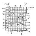
- FIG. 5 there is illustrated a layout or topological view of a portion of a semiconductor chip or wafer 46 in which the circuit of Fig. 4 is fabricated.
- the chip 46 includes a substrate 48 which may be made of P conductivity type silicon.
- An N well 50 is formed in the substrate 48 by, e.g., diffusion or implantation of arsenic.
- a first thin layer of silicon dioxide 52 is grown or deposited over the N well 50 and a second thin layer of silicon dioxide 54 is grown or deposited over substrate 48 outside of the N well 50 but adjacent thereto.
- a thick oxide layer 56 is grown or deposited by any known technique over the substrate 48 outside of the thin silicon dioxide layers 52 and 54.
- a plurality of parallely arranged conductive strips 58 are formed over the insulating layers 52, 54 and 56.
- a source/drain P conductivity type region 60 which may be made by implanting boron into N well 50 with the strips 58 acting as a shield for defining the channel regions of the PMOS devices or transistors, each of which includes two adjacent source/drain regions 60 separated by one of the strips 58 disposed over the transistor's channel region.
- a source/drain N conductivity type region 62 which may be made by implanting arsenic into the substrate 48 with the strips 58 acting as a shield for defining the channel regions of the NMOS devices or transistors, each of which includes two adjacent source/drain regions 62 separated by one of the strips 58 disposed over the transistor's channel region.
- a bus V H which may be made of metal, such as aluminum, and which is the source of potential for the logic circuit on chip 46 is formed over the P channel transistors 58, 60 and insulated from the polysilicon strips 58.
- a ground bus G which also may be made of metal is formed over the N channel transistors 58, 62 and insulated from the polysilicon strips 58.
- Metallic interconnecting strips 64 are also formed over the P and N channel transistors and are insulated from the polysilicon strips 58. Contacts to the source/drain regions 60 and 62 from the metal buses V H and G and the metallic strips 64 are indicated by an X.
- the transistors, including the control gates, of the logic circuit of Fig. 4 are indicated in Fig. 5 by the same reference characters.
- CMOS logic circuit forms a very compact CMOS logic circuit which is readily expandible and which adheres to an automated logic methodology. It is apparent that a finite matrix can be used as a program logic array which is programmable at the mask level. This implementation may be used for any CMOS technology.
- CMOS circuits also applies to static and dynamic NMOS circuits and to dynamic CMOS circuits.
- static NMOS circuits the P channel array or PMOS switch 10 is replaced by, e.g., a single N channel load device or transistor. Stacking is limited in this case due to ratioed constraints.
- Dynamic NMOS and CMOS circuits replace the P channel array 10 with pulsed or clocked load devices of either N or P channel type. Such arrays, however, are leakage and noise sensitive, and must be operated synchronously.
- the matrix 10 of Fig. 4 provides amplification, a full supply voltage being available at the output terminal Q. Additional amplification may be provided in the matrix if desired, to further improve speed.
Landscapes
- Engineering & Computer Science (AREA)
- Power Engineering (AREA)
- Physics & Mathematics (AREA)
- Computer Hardware Design (AREA)
- Computing Systems (AREA)
- General Engineering & Computer Science (AREA)
- Mathematical Physics (AREA)
- Logic Circuits (AREA)
- Metal-Oxide And Bipolar Metal-Oxide Semiconductor Integrated Circuits (AREA)
- Design And Manufacture Of Integrated Circuits (AREA)
Description
- This invention relates to a method of designing a logic circuit according to the preamble of
claim 1. - It is well known that the CMOS technology provides advantages over integrated semiconductor-technologies that use only N channel devices, which may be referred to as NMOS devices, or only P channel devices, which may be referred to as PMOS devices. Some of these advantages include speed and virtually no standby power.
- In static logic designs using only the N channel device technology, complex random logic circuits are either constructed from simple logic blocks or from AND/OR arrays which consume direct current power and are often slow and inefficient in the use of semiconductor surface area.
- A basic logic circuit comprising a matrix having a plurality of circuits of serially arranged P channel devices disposed between a power supply and an output terminal and having a plurality of circuits of serially arranged N channel devices disposed between the output terminal and a point of reference potential, such as ground, is taught in U.S. Patent US-A-3,252,011, filed by B. Zuk on March 16, 1964.
- In U.S. Patent US-A-4,069,426, filed by M. Hirasawa on October 5, 1976, there are taught more complex matrices with more parallel circuits having a higher number of devices for handling a variety of functions. Several logic charts, logic circuits and a truth table are disclosed. Furthermore, this patent discloses logic formulas, one of which relates to the P channel circuit and another which relates to the N channel circuit of a matrix.
- This complementary MOS logic circuit for obtaining second logic signals corresponding to a large number of logic combinations derived from a group of first logic signals, wherein a plurality of series circuits each formed of a plurality of series circuits each formed of a plurality of series-connected first channel type IG-FET's and a plurality of series each formed of a plurality of series-connected second channel type IG-FET's are jointly connected to the output terminal of said complementary MOS type logic circuit. This complementary MOS logic circuit with IG-FET's does not meet the requirements for making high density circuits which produce any desired Boolean logic function at high speeds with a low power.
- In "Electronic design" Volume 15, Number 19, 13 September 1967, pages 81-87 is a nanopower IC-logic with complementary MOS arrays described. In this publication is a method described how to design a logic circuit starting with a trues table which determines the logic functions for the performance of which the logic circuits should serve. The proposed circuits of this document do not solve the objective of this invention, particularly each circuit component or its input respectively can not be accessed individually.
- U.S. Patent US-A-3,945,000 filed by Y. Suzuki et al on July 30, 1974, discloses a logic matrix having all P channel devices formed in one area of a chip and all N channel devices formed in another area of the chip. Also, this patent discloses that the P channel devices are arranged according to a logic function of a certain expression, and the N channel devices are arranged according to a logic function of a different expression.
- U.S. Patent US-A-3,643,232, filed by J. S. Kilby on June 5, 1967, describes a semiconductor chip having a plurality of devices preformed within a semiconductor substrate and then selected devices are interconnected with metallic strips to form desired circuits.
- It is the object of this invention to provide a method of designing a logic circuit which produces any desired Boolean logic function at high speeds with low power and allows automation of logic chip designs from truth tables or logic expressions to the chip layout.
- The solutions of the object are characterized in
claims 1, 4 and 5. - In accordance with the teachings of this invention, a method is provided for reducing an arbitrary Boolean logic function or expression to, e.g., static CMOS circuits by the use of a general matrix of P channel devices and N channel devices which are interconnected in accordance with the terms of Boolean logic expressions derived from a truth table. More specifically, a Boolean expression as a sum-of-products expression is derived from the 1 binary data outputs of a truth table having binary 0 and 1 inputs. This is accomplished by complementing, or barring, in the expression the inputs or literals which are a
binary 1 when the output is 1 and leaving true or unbarred the inputs or literals that are a binary 0. Then each input of a given product term in the expression is applied as a voltage to the gate electrode of a P channel device, which devices are connected in series with one end tied to a source of potential and the other end of the series circuit connected to an output terminal. Each product term is arranged in parallel with other P channel device series circuits to form one half of a complete logic matrix circuit. - Similarly, for the other half of the matrix, a sum-of-products expression giving the binary 0 outputs of a truth table having binary 1's or 0's for an input is found. Each input of a given product term is applied as a voltage to the control gate of an N channel device, which devices are connected in series with one end tied to a potential reference point, such as ground, and the other end of the series circuit is connected to the output terminal. Each product term is arranged in parallel with other N channel device series circuits to form the other half of the logic matrix. Each of the two halves of the matrix can be minimized by factoring out the common literals in the sum-of-product expressions. Redundant P and N channel devices are eliminated and common nodes are tied together.
- The foregoing and other objects, features and advantages of the invention will be apparent from the following and more particular description of the preferred embodiments of the invention, as illustrated in the accompanying drawings.
- Fig. 1
- illustrates a basic schematic diagram within which the circuits produced by the present invention are formed,
- Fig. 2
- illustrates a P channel device array and an N channel device array which may be used in the schematic diagram of Fig. 1,
- Fig. 3
- illustrates an arbitrary logic truth table,
- Fig. 4
- illustrates a logic circuit formed by appropriately interconnecting the P and N channel devices of Fig. 2 which relates to the truth table of Fig. 3, and
- Fig. 5
- is a layout or topological view of a semiconductor chip in which the circuit of Fig. 4 is formed.
- Referring to the drawings in more detail, there is illustrated in Fig. 1 a basic schematic diagram within which the circuits produced by the present invention may be formed. The diagram includes a
first switch 10, made of one or more PMOS devices, connected between a source of potential VH, which may have a potential of +5 volts, and an output terminal Q with input signals IP shown in vectorial form to indicate that a plurality of signals or terms may be applied to the input of thePMOS switch 10. The diagram also includes asecond switch 12, made of one or more NMOS devices, connected between a point of reference potential, such as ground G, and the output terminal Q. The PMOS andNMOS switches PMOS switch 10 is open, theNMOS switch 12 is closed, as indicated in Fig. 1, and vice versa. Thus, it can be seen that in the type of circuit or network illustrated in Fig. 1, there is no static direct current (DC) power dissipated at any time. - Fig. 2 illustrates a convenient arrangement of P channel devices or field effect transistors, each being identified by P, which may be used to form the PMOS switch or
network 10 shown in Fig. 1. A similar arrangement of N channel devices or field effect transistors, each being identified by N, which may be used to form the NMOS switch ornetwork 12 is also shown in Fig. 2. - Fig. 3 illustrates an arbitrary logic truth table having four input signals or literals A, B, C and D and an indication of the output signal Q, a binary 1 or 0, arranged in four rows and four columns, for the various combinations of inputs of the four literals A, B, C and D. The Boolean expression for this truth table may be found to be

- In accordance with the teachings of this invention, from a truth table, such as the table of Fig. 3, a Boolean logic expression QP is derived using 1 binary data outputs having binary 1's and 0's as an input. The inputs or literals which are a
binary 1 are complemented, or barred, when the output is abinary 1, with the inputs or literals which are a binary 0 remaining true or unbarred. Thus, by referring to the truth table in Fig. 3, it can be seen that
- By using known algebraic theorems and by factoring out the common inputs in the sum-of-product expression,

- Having derived this Boolean expression, a voltage representative of each input of a given product term of the expression is applied to the gate electrode of a P channel device P in the PMOS switch or
network 10 which are connected in series with one end tied to the source of potential VH and the other end of the series circuit connected to the output terminal Q. Each product term is arranged as a series circuit between the potential source VH and the output terminal Q and in parallel with all other PMOS device series circuits representing other product terms of the expression. - By referring to Fig. 4 of the drawings, it can be seen that the inputs
A , B, C and D of one term of the expression QP are connected to the control gates oftransistors transistor 22, while the inputsD ,C andB of this other term are connected to the control gates oftransistors transistor 22 between the potential source VH and the output terminal Q, in accordance with the terms of the expression QP indicated by formula (2) identified hereinabove. It should be noted that input A could be connected to the gate electrodes of three P channel devices P with each of thetransistors common transistor 22 to form the PMOS switch ornetwork 10, in accordance with the terms of expression QP indicated by formula (1) identified hereinabove. However, since fewer transistors are used when forming the PMOS switch ornetwork 10 in accordance with the terms of expression QP indicated by formula (2), the circuit arrangement for formula (2) is preferred. - Further in accordance with the teachings of this invention, from the truth table in Fig. 3, a Boolean logic expression QN is derived using 0 binary data outputs having binary 1's and 0's as inputs. The inputs or literals which are binary 0 are complemented, or barred, when the output is a
binary 0, with the inputs or literals which are a 1 remaining true or unbarred. Thus, by again referring to the truth table in Fig. 3, it can be seen that
- By using known theorems and by factoring out the common inputs in the sum-of-product expression,

- With this Boolean expression QN having been derived from the truth table, a voltage representative of each input of a given product term is applied to the gate electrode of an N channel device N in NMOS switch or
network 12 which are connected in series with one end of the series circuit tied to the point of reference potential G and the other end connected to the output terminal Q. Each product term is arranged as a series circuit between the point of reference potential G and the output terminal Q and in parallel with all other NMOS device series circuits representing other product terms of the expression QN. - By again referring to Fig. 4 of the drawings, it can be seen that the inputs
A ,B ,C andD of one term of the expression QN are connected to the control gates oftransistors transistor 38, while the inputs D, C and B of this other term are connected to the control gates oftransistors transistor 38 between the point of reference potential G and the output terminal Q, in accordance with the terms of the expression QN indicated by formula (4) identified hereinabove. It should be noted that input A could be connected to the gate electrode of three N channel devices N with each of thetransistors common transistor 38 to form the NMOS switch ornetwork 12, in accordance with the terms of expression QN indicated by formula (3) identified hereinabove. Generally, since fewer devices are used, the circuit formed in accordance with formula (4) is preferred. - Although the circuit of Fig. 4 was formed from expressions QP and QN, formulas (2) and (4), respectively, derived from the truth table in Fig. 3, it should be understood that other logic circuits may be designed in a similar manner from truth tables which differ from that of Fig. 3. Not only can the truth table of Fig. 3 have the input literals with different outputs, but the number of inputs may be fewer or greater than four, as desired. It can be seen that with four inputs or literals, as in the truth table of Fig. 3, there are four columns and four rows of P channel transistors P and four columns and four rows of N channel transistors N in Fig. 4, although many of these transistors are not used for the logic circuit formed in Fig. 4 and, therefore, are available for other circuits.
- In Fig. 5, there is illustrated a layout or topological view of a portion of a semiconductor chip or
wafer 46 in which the circuit of Fig. 4 is fabricated. Thechip 46 includes asubstrate 48 which may be made of P conductivity type silicon. An N well 50 is formed in thesubstrate 48 by, e.g., diffusion or implantation of arsenic. A first thin layer ofsilicon dioxide 52 is grown or deposited over the N well 50 and a second thin layer ofsilicon dioxide 54 is grown or deposited oversubstrate 48 outside of the N well 50 but adjacent thereto. Athick oxide layer 56 is grown or deposited by any known technique over thesubstrate 48 outside of the thin silicon dioxide layers 52 and 54. A plurality of parallely arrangedconductive strips 58, preferably made of doped polysilicon, are formed over the insulatinglayers silicon dioxide layer 52 and adjacent to each side of eachstrip 58 is a source/drain Pconductivity type region 60 which may be made by implanting boron into N well 50 with thestrips 58 acting as a shield for defining the channel regions of the PMOS devices or transistors, each of which includes two adjacent source/drain regions 60 separated by one of thestrips 58 disposed over the transistor's channel region. Under the second thinsilicon dioxide layer 54 and adjacent to each side of eachstrip 58 is a source/drain Nconductivity type region 62 which may be made by implanting arsenic into thesubstrate 48 with thestrips 58 acting as a shield for defining the channel regions of the NMOS devices or transistors, each of which includes two adjacent source/drain regions 62 separated by one of thestrips 58 disposed over the transistor's channel region. A bus VH which may be made of metal, such as aluminum, and which is the source of potential for the logic circuit onchip 46 is formed over theP channel transistors N channel transistors drain regions metallic strips 64 are indicated by an X. The transistors, including the control gates, of the logic circuit of Fig. 4 are indicated in Fig. 5 by the same reference characters. - It can be seen that the structure of Fig. 5 forms a very compact CMOS logic circuit which is readily expandible and which adheres to an automated logic methodology. It is apparent that a finite matrix can be used as a program logic array which is programmable at the mask level. This implementation may be used for any CMOS technology.
- It should be understood that this methodology for rapidly preparing logic circuits from truth tables is valid for any random logic function and also for common logic building blocks such as NOR, NAND, AOI, XOR and multiplexers. The stacking of devices is limited only by performance. For several levels, the output may be buffered and amplified, if desired. The speed of operation of this circuit is enhanced by the processing of the input data in parallel and by its compactness. Static DC power is not dissipated at any time.
- It should also be understood that the methodology described hereinabove in connection with static CMOS circuits also applies to static and dynamic NMOS circuits and to dynamic CMOS circuits. For static NMOS circuits, the P channel array or
PMOS switch 10 is replaced by, e.g., a single N channel load device or transistor. Stacking is limited in this case due to ratioed constraints. Dynamic NMOS and CMOS circuits replace theP channel array 10 with pulsed or clocked load devices of either N or P channel type. Such arrays, however, are leakage and noise sensitive, and must be operated synchronously. - The
matrix 10 of Fig. 4 provides amplification, a full supply voltage being available at the output terminal Q. Additional amplification may be provided in the matrix if desired, to further improve speed.
Claims (8)
- Method of designing a logic circuit which satisfies the requirements of a truth table having a given number of binary input literals and binary output values which comprises the following steps:
forming inputs of first and second product terms of a first Boolean function QP from a truth table by complementing the binary input literals which are a "1" when the output value is a binary "1" and using the true binary input literal which is a "0" when the output value is a binary "1" by forming first and second series circuits respectively comprising a plurality of P channel transistors and connecting them in parallel between a voltage source and an output terminal and by applying a voltage representative of each input of said first and second product terms of said first Boolean function to control gates of said plurality of P channel transistors,
forming inputs of first and second product terms of a second Boolean function QN from said truth table by complementing the binary input literals which are a "0" when the output value is a binary "0" and using the true binary input literal which is a "1" when the output value is a binary "0" by forming third and fourth series circuits respectively comprising a plurality of N channel transistors and connecting them in parallel between said output terminal and a point of reference potential and by applying a voltage representative of each input of said first and second product term of said second Boolean function to control gates of said plurality of N channel transistors. - Method as set forth in claim 1,
characterized in, that one of said formed inputs is common to the first and second terms of said first Boolean function and that for said first and second series circuits a common P channel transistor is formed. - Method as set forth in claim 1,
characterized in, that one of said inputs is common to the first and second terms of said second Boolean function and that for said third and fourth series circuits a common N channel transistor is formed. - Method as set forth in claim 1,
characterized by
a voltage representative of each input of each product term of said first Boolean function which is applied to control gates of a plurality of P channel transistors interconnecting them to form a plurality of series circuits,
connecting said plurality of series circuits in a parallel arrangement between a voltage source and an output terminal,
applying a voltage representative of each input of each product term of said second Boolean function to control gates of a plurality of N channel transistors interconnected to form a plurality of series circuits, and
connecting said plurality of series circuits of N channel transistors in a parallel arrangement between said output terminal and a point of reference potential. - Method as set forth in claim 4, characterized by
forming a first matrix (10) of a plurality of P channel field effect transistors, and forming a second matrix (12) of a plurality of P channel field effect transistors is processed, where one of the inputs is common to two of said product terms of said first Boolean function and at least two of the series circuits of P or N channel transistors have a common P or N channel transistor respectively. - Method of designing a logic circuit as set forth in claims 1 or 4, characterized by
forming the first Boolean function QP to a form having a minimum number of inputs,
forming the inputs of a plurality of product terms of a second Boolean function QN from said truth table by complementing the binary input literals which are a 0 when the output value is a binary 0 and using the true binary input literals which are a 1 when the output value is a binary 0,
reducing said second Boolean function QN to a form having a minimum number of inputs,
applying a voltage representative of each of said minimum number of inputs of said first Boolean function QP to control gates of a plurality of P channel transistors interconnected to form a plurality of series circuits,
connecting the plurality of series circuits in a parallel arrangement between a voltage source and an output terminal,
applying a voltage representative of each of said minimum number of inputs of said second Boolean function QN to control gates of a plurality of N channel transistors interconnected to form a plurality of series circuits, and
connecting the plurality of series circuits of N channel transistors in parallel arrangement between said output terminal and a point of reference potential. - Method as set forth in claim 5, characterized by
forming said second matrix (12) of N channel transistors in a first region of a P type conductivity semiconductor substrate,
forming a N well in a second region of said substrate adjacent to said first region, and forming said first matrix (10) of P channel regions in said N well. - Method of designing a logic circuit as set forth in claim 6, characterized by
forming a plurality of series circuits of P channel transistors in parallel between a voltage source and an output terminal,
applying a voltage representative of each input of each product term of said reduced first function to the control gates of the P channel transistors of a respective one of said series circuits,
forming a second function having a plurality of product terms from said truth table, each of said terms having a number of inputs equal to said given number and being formed by complementing the binary input literals which are a 0 when the output value is a binary 0 and using the true binary input literal which is a 1 when the output value is a 0,
reducing said second function to a form having a minimum number of product terms,
forming a plurality of series circuits of N channel transistors in parallel between a point of reference potential and said output terminal, and
applying a voltage representative of each input of each product term of said reduced second function to the control gates of the N channel transistors of a respective one of said series circuits of N channel transistors.
Applications Claiming Priority (2)
| Application Number | Priority Date | Filing Date | Title |
|---|---|---|---|
| US06/554,148 US4591993A (en) | 1983-11-21 | 1983-11-21 | Methodology for making logic circuits |
| US554148 | 1983-11-21 |
Publications (3)
| Publication Number | Publication Date |
|---|---|
| EP0142766A2 EP0142766A2 (en) | 1985-05-29 |
| EP0142766A3 EP0142766A3 (en) | 1986-07-23 |
| EP0142766B1 true EP0142766B1 (en) | 1991-09-25 |
Family
ID=24212228
Family Applications (1)
| Application Number | Title | Priority Date | Filing Date |
|---|---|---|---|
| EP84113322A Expired - Lifetime EP0142766B1 (en) | 1983-11-21 | 1984-11-06 | A method for making logic circuits |
Country Status (4)
| Country | Link |
|---|---|
| US (1) | US4591993A (en) |
| EP (1) | EP0142766B1 (en) |
| JP (1) | JPS60117757A (en) |
| DE (1) | DE3485112D1 (en) |
Families Citing this family (24)
| Publication number | Priority date | Publication date | Assignee | Title |
|---|---|---|---|---|
| US4703435A (en) * | 1984-07-16 | 1987-10-27 | International Business Machines Corporation | Logic Synthesizer |
| US4700316A (en) * | 1985-03-01 | 1987-10-13 | International Business Machines Corporation | Automated book layout in static CMOS |
| JPH0668756B2 (en) * | 1985-04-19 | 1994-08-31 | 株式会社日立製作所 | Circuit automatic conversion method |
| US4792909A (en) * | 1986-04-07 | 1988-12-20 | Xerox Corporation | Boolean logic layout generator |
| US4745084A (en) * | 1986-11-12 | 1988-05-17 | Vlsi Technology, Inc. | Method of making a customized semiconductor integrated device |
| US4782249A (en) * | 1987-08-03 | 1988-11-01 | General Electric Company | Static CMOS programmable logic array |
| US4870598A (en) * | 1987-08-04 | 1989-09-26 | Texas Instruments Incorporated | Comprehensive logic circuit layout system |
| US5150309A (en) * | 1987-08-04 | 1992-09-22 | Texas Instruments Incorporated | Comprehensive logic circuit layout system |
| US5119313A (en) * | 1987-08-04 | 1992-06-02 | Texas Instruments Incorporated | Comprehensive logic circuit layout system |
| US4916627A (en) * | 1987-12-02 | 1990-04-10 | International Business Machines Corporation | Logic path length reduction using boolean minimization |
| US5173864A (en) * | 1988-08-20 | 1992-12-22 | Kabushiki Kaisha Toshiba | Standard cell and standard-cell-type integrated circuit |
| US4928160A (en) * | 1989-01-17 | 1990-05-22 | Ncr Corporation | Gate isolated base cell structure with off-grid gate polysilicon pattern |
| US5243538B1 (en) * | 1989-08-09 | 1995-11-07 | Hitachi Ltd | Comparison and verification system for logic circuits and method thereof |
| US5237513A (en) * | 1989-11-20 | 1993-08-17 | Massachusetts Institute Of Technology | Optimal integrated circuit generation |
| US5084824A (en) * | 1990-03-29 | 1992-01-28 | National Semiconductor Corporation | Simulation model generation from a physical data base of a combinatorial circuit |
| US5313119A (en) * | 1991-03-18 | 1994-05-17 | Crosspoint Solutions, Inc. | Field programmable gate array |
| US5524082A (en) * | 1991-06-28 | 1996-06-04 | International Business Machines Corporation | Redundancy removal using quasi-algebraic methods |
| US5416719A (en) * | 1992-12-17 | 1995-05-16 | Vlsi Technology, Inc. | Computerized generation of truth tables for sequential and combinatorial cells |
| JP3182036B2 (en) * | 1994-02-16 | 2001-07-03 | 松下電器産業株式会社 | Logic synthesis method and logic synthesis device |
| US5465055A (en) * | 1994-10-19 | 1995-11-07 | Crosspoint Solutions, Inc. | RAM-logic tile for field programmable gate arrays |
| US5629636A (en) * | 1994-10-19 | 1997-05-13 | Crosspoint Solutions, Inc. | Ram-logic tile for field programmable gate arrays |
| US6240542B1 (en) * | 1998-07-14 | 2001-05-29 | Lsi Logic Corporation | Poly routing for chip interconnects with minimal impact on chip performance |
| US7877711B2 (en) * | 2006-03-01 | 2011-01-25 | Nangate A/S | Methods of deriving switch networks |
| US8370115B2 (en) * | 2007-05-15 | 2013-02-05 | Broadcom Corporation | Systems and methods of improved boolean forms |
Citations (1)
| Publication number | Priority date | Publication date | Assignee | Title |
|---|---|---|---|---|
| EP0130363A2 (en) * | 1983-06-27 | 1985-01-09 | International Business Machines Corporation | Differential logic circuit implemented in complementary transistor technology |
Family Cites Families (7)
| Publication number | Priority date | Publication date | Assignee | Title |
|---|---|---|---|---|
| US3252011A (en) * | 1964-03-16 | 1966-05-17 | Rca Corp | Logic circuit employing transistor means whereby steady state power dissipation is minimized |
| US3643232A (en) * | 1967-06-05 | 1972-02-15 | Texas Instruments Inc | Large-scale integration of electronic systems in microminiature form |
| NL176029C (en) * | 1973-02-01 | 1985-02-01 | Philips Nv | INTEGRATED LOGIC CIRCUIT WITH COMPLEMENTARY TRANSISTORS. |
| JPS5620734B2 (en) * | 1973-07-31 | 1981-05-15 | ||
| JPS5244551A (en) * | 1975-10-06 | 1977-04-07 | Toshiba Corp | Logic circuit |
| US4356504A (en) * | 1980-03-28 | 1982-10-26 | International Microcircuits, Inc. | MOS Integrated circuit structure for discretionary interconnection |
| US4482810A (en) * | 1982-09-30 | 1984-11-13 | Storage Technology Partners | Electron beam exposure system |
-
1983
- 1983-11-21 US US06/554,148 patent/US4591993A/en not_active Expired - Lifetime
-
1984
- 1984-07-20 JP JP59149812A patent/JPS60117757A/en active Granted
- 1984-11-06 DE DE8484113322T patent/DE3485112D1/en not_active Expired - Fee Related
- 1984-11-06 EP EP84113322A patent/EP0142766B1/en not_active Expired - Lifetime
Patent Citations (1)
| Publication number | Priority date | Publication date | Assignee | Title |
|---|---|---|---|---|
| EP0130363A2 (en) * | 1983-06-27 | 1985-01-09 | International Business Machines Corporation | Differential logic circuit implemented in complementary transistor technology |
Non-Patent Citations (1)
| Title |
|---|
| Electro/80 Conference Record, May 13 - 15, 1980, Boston MA, Vol.5, p. 1-7 * |
Also Published As
| Publication number | Publication date |
|---|---|
| EP0142766A2 (en) | 1985-05-29 |
| EP0142766A3 (en) | 1986-07-23 |
| JPH0544853B2 (en) | 1993-07-07 |
| US4591993A (en) | 1986-05-27 |
| JPS60117757A (en) | 1985-06-25 |
| DE3485112D1 (en) | 1991-10-31 |
Similar Documents
| Publication | Publication Date | Title |
|---|---|---|
| EP0142766B1 (en) | A method for making logic circuits | |
| US7466163B2 (en) | Look-up table structure with embedded carry logic | |
| US7656190B2 (en) | Incrementer based on carry chain compression | |
| US7239174B2 (en) | Programmable interconnect structures | |
| US7285984B2 (en) | Look-up table structure with embedded carry logic | |
| US20060132175A1 (en) | Look-up table based logic macro-cells | |
| US5671397A (en) | Sea-of-cells array of transistors | |
| EP0809362A2 (en) | Logic circuit and its fabrication method | |
| US7336097B2 (en) | Look-up table structure with embedded carry logic | |
| EP0283655B1 (en) | A method of combining gate array and standard cell circuits on a common semiconductor chip | |
| EP0290857B1 (en) | A bias device for achieving voltage independent capacitance | |
| US4833347A (en) | Charge disturbance resistant logic circuits utilizing true and complement input control circuits | |
| US5814846A (en) | Cell apparatus and method for use in building complex integrated circuit devices | |
| EP0092176B1 (en) | Basic cell for integrated-circuit gate arrays | |
| EP1723723B1 (en) | Logic basic cell, logic basic cell array and logic device | |
| EP0117310B1 (en) | Transistor array arrangement | |
| US4652777A (en) | CMOS programmable logic array | |
| WU et al. | Invited paper A unified theory for MOS circuit design—switching network logic | |
| US4880754A (en) | Method for providing engineering changes to LSI PLAs | |
| US4952824A (en) | Ion implantation programmable logic device | |
| US5701021A (en) | Cell architecture for mixed signal applications | |
| US4870471A (en) | Complementary metal-oxide semiconductor integrated circuit device with isolation | |
| Tomisawa et al. | A 920 gate DSA MOS masterslice | |
| Rajender et al. | VLSI DESIGN | |
| GB2121601A (en) | Uncommitted logic integrated circuit array |
Legal Events
| Date | Code | Title | Description |
|---|---|---|---|
| PUAI | Public reference made under article 153(3) epc to a published international application that has entered the european phase |
Free format text: ORIGINAL CODE: 0009012 |
|
| 17P | Request for examination filed |
Effective date: 19841211 |
|
| AK | Designated contracting states |
Designated state(s): DE FR GB |
|
| PUAL | Search report despatched |
Free format text: ORIGINAL CODE: 0009013 |
|
| RHK1 | Main classification (correction) |
Ipc: H03K 19/173 |
|
| AK | Designated contracting states |
Kind code of ref document: A3 Designated state(s): DE FR GB |
|
| 17Q | First examination report despatched |
Effective date: 19871120 |
|
| GRAA | (expected) grant |
Free format text: ORIGINAL CODE: 0009210 |
|
| AK | Designated contracting states |
Kind code of ref document: B1 Designated state(s): DE FR GB |
|
| REF | Corresponds to: |
Ref document number: 3485112 Country of ref document: DE Date of ref document: 19911031 |
|
| ET | Fr: translation filed | ||
| PLBE | No opposition filed within time limit |
Free format text: ORIGINAL CODE: 0009261 |
|
| STAA | Information on the status of an ep patent application or granted ep patent |
Free format text: STATUS: NO OPPOSITION FILED WITHIN TIME LIMIT |
|
| 26N | No opposition filed | ||
| PGFP | Annual fee paid to national office [announced via postgrant information from national office to epo] |
Ref country code: GB Payment date: 19941013 Year of fee payment: 11 |
|
| PGFP | Annual fee paid to national office [announced via postgrant information from national office to epo] |
Ref country code: FR Payment date: 19941103 Year of fee payment: 11 |
|
| PGFP | Annual fee paid to national office [announced via postgrant information from national office to epo] |
Ref country code: DE Payment date: 19941201 Year of fee payment: 11 |
|
| PG25 | Lapsed in a contracting state [announced via postgrant information from national office to epo] |
Ref country code: GB Effective date: 19951106 |
|
| GBPC | Gb: european patent ceased through non-payment of renewal fee |
Effective date: 19951106 |
|
| PG25 | Lapsed in a contracting state [announced via postgrant information from national office to epo] |
Ref country code: FR Effective date: 19960731 |
|
| PG25 | Lapsed in a contracting state [announced via postgrant information from national office to epo] |
Ref country code: DE Effective date: 19960801 |
|
| REG | Reference to a national code |
Ref country code: FR Ref legal event code: ST |