EP0142555B1 - Dual band phased array using wideband elements with diplexer - Google Patents
Dual band phased array using wideband elements with diplexer Download PDFInfo
- Publication number
- EP0142555B1 EP0142555B1 EP84902183A EP84902183A EP0142555B1 EP 0142555 B1 EP0142555 B1 EP 0142555B1 EP 84902183 A EP84902183 A EP 84902183A EP 84902183 A EP84902183 A EP 84902183A EP 0142555 B1 EP0142555 B1 EP 0142555B1
- Authority
- EP
- European Patent Office
- Prior art keywords
- dual band
- waveguide
- diplexer
- waveguide device
- disposed
- Prior art date
- Legal status (The legal status is an assumption and is not a legal conclusion. Google has not performed a legal analysis and makes no representation as to the accuracy of the status listed.)
- Expired - Lifetime
Links
Images


Classifications
-
- H—ELECTRICITY
- H01—ELECTRIC ELEMENTS
- H01Q—ANTENNAS, i.e. RADIO AERIALS
- H01Q3/00—Arrangements for changing or varying the orientation or the shape of the directional pattern of the waves radiated from an antenna or antenna system
- H01Q3/26—Arrangements for changing or varying the orientation or the shape of the directional pattern of the waves radiated from an antenna or antenna system varying the relative phase or relative amplitude of energisation between two or more active radiating elements; varying the distribution of energy across a radiating aperture
- H01Q3/30—Arrangements for changing or varying the orientation or the shape of the directional pattern of the waves radiated from an antenna or antenna system varying the relative phase or relative amplitude of energisation between two or more active radiating elements; varying the distribution of energy across a radiating aperture varying the relative phase between the radiating elements of an array
-
- H—ELECTRICITY
- H01—ELECTRIC ELEMENTS
- H01P—WAVEGUIDES; RESONATORS, LINES, OR OTHER DEVICES OF THE WAVEGUIDE TYPE
- H01P5/00—Coupling devices of the waveguide type
- H01P5/08—Coupling devices of the waveguide type for linking dissimilar lines or devices
- H01P5/10—Coupling devices of the waveguide type for linking dissimilar lines or devices for coupling balanced with unbalanced lines or devices
- H01P5/103—Hollow-waveguide/coaxial-line transitions
-
- H—ELECTRICITY
- H01—ELECTRIC ELEMENTS
- H01Q—ANTENNAS, i.e. RADIO AERIALS
- H01Q13/00—Waveguide horns or mouths; Slot antennas; Leaky-waveguide antennas; Equivalent structures causing radiation along the transmission path of a guided wave
- H01Q13/06—Waveguide mouths
-
- H—ELECTRICITY
- H01—ELECTRIC ELEMENTS
- H01Q—ANTENNAS, i.e. RADIO AERIALS
- H01Q21/00—Antenna arrays or systems
- H01Q21/30—Combinations of separate antenna units operating in different wavebands and connected to a common feeder system
-
- H—ELECTRICITY
- H01—ELECTRIC ELEMENTS
- H01Q—ANTENNAS, i.e. RADIO AERIALS
- H01Q5/00—Arrangements for simultaneous operation of antennas on two or more different wavebands, e.g. dual-band or multi-band arrangements
Abstract
Description
- This invention is directed to waveguide array systems, in general, and to dual-band, wideband, shared aperture waveguide systems, in particular.
- There are many known methods, devices and systems associated with waveguide systems, in general, and radar systems, in particular. For the most part, the known systems and devices are directed to single band arrays which operate on only one frequency signal at a time. These signals may be in the microwave frequency range, e.g., 3.5 GHz or the like. Typically, the known systems are of a relatively narrow scan capability.
- Many of these systems include waveguide devices which are utilized with coaxial cables as the input or output means. In these types of systems, various types of transition devices are used to couple the waveguide to the cable.
- In most cases the radar systems include a single band device. That is, the system operates on only one frequency band. Thus, two (or more) array apertures are required in order to process multiple frequencies. In the past, this has caused the multi-frequency systems to have multiple apertures with the attendant increases in cost, weight, size and the like. Thus, these systems have been disadvantageous for utilization in many applications.
- Also, in the past, attempts have been made to provide systems wherein a single aperture has been shared by multiple antenna arrays. However, these prior systems were generally of poor quality due to interference and crosscoupling. The best known example of this technique was a twin-dielectric-slab-loaded waveguide array with each frequency band fed by a separate feeding probe as described by Mailloux et al (IEEE Transactions on Antennas and Propagation, Volume AP-27,
No 2, March 1979). However, the two signal bands are difficult to isolate and the impedance matching is difficult resuling in relatively high VSWR, e.g. 3:1 or greater. - Prior art documents considered the most pertinent are as follows.
- U.S. Patent 3,825,932 is directed to a multi-frequency waveguide antenna in which the waveguide radiator elements have a cut-off frequency between two operating frequencies of the antenna. At the lower frequency, the waveguides are terminated to function as evanescent mode resonators giving a first passband centered on the lower frequency. At the higher frequency, the waveguides are propagating and are terminated to give a second passband centered on the higher frequency.
- DE 1,128,490 appears to show a transition using several transition devices.
- U.S. Patent 4,240,155 is directed to a diplexer and multiplexer device. The device combines a plurality of different frequency signals for transmission in a common transmission line by a series of hybrid coupler devices.
- U. S. Patent 3,725,824; Woodward; COMPACT WAVEGUIDE-COAX TRANSITION. This patent is directed to a waveguide-to-coaxial cable transition device using a half-height waveguide, a tapered ridge waveguide section, and a 90° coaxial cable connection.
- U. S. Patent 3,758,886; Landry et al; VERSATILE IN LINE WAVEGUIDE TO COAX TRANSITION. This patent is directed to a microwave transition device which includes a hook-shaped exciter and a U-shaped dielectric loading transformer.
- U. S. Patent 3,431,515; Brediger et al; MICROWAVE TRANSITION APPARATUS. This patent is directed to a microwave transition apparatus which includes a dielectric element shaped to match the impedances of the coax line and waveguide and to provide an asymmetrical load therebetween to alter the propagating wave.
- U. S. Patent 4,375,052; Anderson; POLARIZATION ROTA-TABLE ANTENNA FEED. This patent is directed to a wave polarization rotary section which includes a ridge loaded wave-guide transaction section.
- U. S. Patent 4,231,000; Schuegraf; ANTENNA FEED SYSTEM FOR DOUBLE POLARIZATION. This patent is directed to an antenna system for double polarization in two high frequency bands and includes a polarization filter with an antenna and terminal and two directional terminals for circularly polarized waves.
- U. S. Patent 4,029,902; Bell, et al; CONTIGUOUS CHANNEL MULTIPLEXER. This patent is directed to a multiplexer for combining a plurality of microwave signal channels for transmission over a common transmission path.
- U. S. Patent 3,034,076; Tomiyasu; MICROWAVE DIPLEXER. This patent is directed to an apparatus for coupling (or decoupling) two different frequency microwave signals relative to a single antenna.
- U. S. Patent 3,252,113; Veltrop; BROADBAND HYBRID DIPLEXER. This patent is directed to diplexer frequency branching networks.
- "BROAD-BAND IMPEDANCE MATCHING OF RECTANGULAR WAVEGUIDE PHASED ARRAYS," Chen, IEEE Trans. Antennas and Propogation, Vol AP-21, No. 3, May 1973, pp. 298-302.
- "ANALYSIS OF A DUAL-FREQUENCY ARRAY TECHNIQUE"; Mailloux, et al, IEEE Trans. Antennas and Prop., Vol. AP-27, No. 2, March 1979, pp. 130-136.
- "ANALYSIS OF INTERLEAVED ARRAYS OF WAVEGUIDE ELEMENTS," Hsiao, IEEE Trans. Antennas and Prop., Vol. AP-19, No. 6, Nov. 1971, pp 729-735.
- No significance is implied by the order of the listing.
- According to the present invention there is provided a dual band antenna array comprising a waveguide device having a wideband aperture therein, an iris having a selected opening disposed therein, and a dual band transitioning device coupled to the waveguide device for transferring energy into and out of the waveguide device, the array characterised in that:
- (i) the antenna array is arranged for operation over approximately an octave bandwidth encompassing first and second distinct frequency bands;
- (ii) the transitioning device is a coaxial-to-waveguide transition arranged for propagating operation over each of the first and second frequency bands;
- (iii) a dielectric sheet having a predetermined dielectric constant is disposed in front of the aperture for impedance matching over the first and second frequency bands;
- (iv) the transitioning device is a wide band device arranged for operating over the first and second distinct frequency bands and efficiently transitioning energy in said first and second frequency bands into and out of the waveguide device via a single transition port;
- (v) a diplexer device is coupled to the single port of the wide band transitioning device by coaxial cable for receiving signals in said respective first and second frequency bands at a first diplexer port and separating the signals into signals of frequencies in the first frequency band at a second diplexer port and of frequencies in the second frequency band at a third diplexer port;
- (vi) at least two feed networks are coupled respectively to the second and third diplexer ports for operating on respective signals in the respective first and second frequency bands; and
- (vii) the waveguide device is selected so that the waveguide cutoff frequency is below either frequency band and is suitable for low-loss, propagating operation over each of the first and second frequency bands.
- In a preferred embodiment, the invention utilizes an open-ended waveguide array which can operate over approximately an octave bandwidth encompassing two adjacent microwave bands. The radiating element is well-matched over an octave in bandwidth for the wide range of scan angles of interest. After the dual band signals are received efficiently by the wide-band radiating element, the signals are separated into the two frequency channels by a diplexer. Separate feed networks are used to process the signals of the two bands. It is shown that a good match can be obtained over the desired bandwidth and scanning range. A desirable dual band transition is included to provide optimal match at both of the frequency bands by fine tuning the matching elements. A diplexer is used with the system to provide the necessary isolation between the two frequency bands.
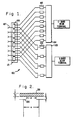
- Figure 1 is a block diagram of a dual band antenna system capable of forming two simultaneously and independently steerable beams.
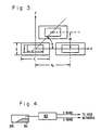
- Figures 2 and 3 are schematic representations of a radiating structure aperture.
- Figure 4 is a schematic representation of the system of the instant invention.
- Figures 5-10 are Smith charts which show the calculated impedance of the wideband waveguide of the instant invention for different values of fH.
- Figures 11-13 show different embodiments of coaxial-to-waveguide transitions of the instant invention.
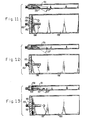
- Figures 14-16 are charts which show the measured return loss of the transitions shown in Figures 11-13, respectively.
- Figure 17 is a block diagram of a diplexer configuration used with the instant invention.
- Referring to Figure 1, there is shown a block diagram representation of a dual
band antenna system 100 which incorporates the teachings of this invention. This system is capable of forming two simultaneously and independently steerable beams. Typically, thesystem 100 includes a radiatingaperture array 101 which is capable of being shared by the two adjacent frequency bands, such as S-band signals and C-band signals.Array 101 includes radiator anddual transitions 107. Thearray 101 includes a plurality ofdiplexers 106 connected to a plurality of C-band phase shifters 102 and a plurality of S-band phase shifters 103 in a conventional manner. The respective phase shifters are then connected to the C-bandcorporate feed 104 and the S-bandcorporate feed 105. In the S-band feed, block feeding may be used to save the cost of phase shifters and drivers, without causing the grating lobe formation. Thus, only four S-band phase shifters 103 are required in this embodiment. The corporate feeds are then connected to the C-band beam terminal, respectively. - The design concept of the present invention utilizes an ultra-wide bandwidth radiating element which can operate over approximately an octave bandwith encompassing, for example, both S-band and C-band. In general, it is very difficult to design a well-matched radiating element over an octave in bandwidth for wide scan coverage. However, an open-ended rectangular waveguide element which is suitable for the present application has been designed and is shown schematically in Figure 2. This waveguide element has an
inductive iris 200 loading at the aperture. In addition, an impedance matchingdielectric radome sheet 201 is provided in front of the waveguide aperture. The geometry of the radiating aperture is suggested in Figure 2. The impedance characteristics of the radiating element have been determined over a frequency range of 0.6 fh to 1.0 fh where fh is the highest frequency of interest (See Figures 5-10). A VSWR of about 2:1 has been achieved as shown by Figures 5-10. When the application of the system does not require a good match for the frequencies between the S-band and C-band frequencies, the impedance match at the two discrete S-band and C-band frequencies can be tuned empirically in order to improve performance. The wideband capability of this radiating element has been reported by N. S. Wong, et al, "Investigation of Use of Superimposed Surface Wave Modes", Final Report prepared by Hughes Aircraft Company under contract F 1962-68-C-0185, Report No. AFCRL-70-0183, 1 February 1970. - Typical design criteria for the aperture and
dielectric radome sheet 201 for the S-band C-band example are set out herewith: - Dielectric Sheet Radome:
- Air gap t₁ = 0.0884 λh
Sheet thickness t₂ = 0.0276 λh
Sheet dielectric constant εr = 7.50 - These criteria are discussed in the paper by Chen which is cited in the Information Disclosure Statement. Moreover, as noted above, empirical tuning gives matching techniques for the aperture which can improve on the aperture constructed in accordance with the calculations of Chen or Wong, et al, supra.
- Referring now to Figure 3, there is shown one example of the geometry of the wideband radiating array aperture of the instant invention. This example of the aperture design is given in terms of wavelength λh in the following table.

- In element spacings, dx is the horizontal, center-to-center spacing of the array elements; dy is the vertical center-to-center spacing of the elements; and α is the angle (measured from the horizontal) between the centers of elements in adjacent tiers.
- In the waveguide dimensions, a and b are the width and heighth, respectively, of the waveguide; a' and b' are the width and heighth, respectively, of the iris.
- In one embodiment of the invention, an array was constructed with the approximate waveguide dimensions:


and element spacings:


- This array operated with the approximate S-band (3.0-4.0 GHz),C-band (5.0-6.0 GHz) described herein.
- Referring to Figure 4, there is shown a schematic representation of the system of the instant invention. In particular, the utilization of the ultra wideband element design for the dual-band, phased array application is illustrated. The dual band signals can be received efficiently by the radiating
element 300. A wideband coaxial-to-waveguide transition 301 can be used to carry the signals to a network of suitable configuration (e.g. TEM) so that adiplexer 302 can be constructed easily. The dual band signals are separated at thediplexer 302 and can be processed in separate bands e.g. S-band and C-band feed networks as indicated in Figure 4. The advantage of this dual band phased array technique includes not only good impedance characteristics but also the absence of grating lobe formation and the crosscoupling problems of the prior art. Also, this Figure represents the "end-on" configuration which is most useful in a multi-tier multi-element array. - The impedance characteristics of the radiating elements shown in Figure 3 have been computed and typical admittance characteristics are shown in the Smith charts reproduced in Figures 5 - 10. In particular, at frequency f - 1.0 fH, the radiation admittance of this design as a function of scan coverage is shown in Figure 5. At frequency f=0.946fH, the radiation admittance is shown in Figure 6. At frequency f = 0.893fH, the radiation admittance is shown in Figure 7. At frequency f = 0.643fH, the radiation admittance is shown in Figure 8. At frequency f = 0.589fH, the radiation admittance is shown in Figure 9. At frequency f = 0.536fH, the radiation admittance is shown in Figure 10.
- It should be understood that fH is the highest frequency in the particular bands of interest. Thus, in the preferred embodiment, 1.0 fH = 5.60 GHz. From this it can be calculated that:

- From the impedance curves presented in Figures 5-10, it is seen that a 2:1 VSWR circle can be drawn around the C-band impedances (for frequencies from 0.893 fH to 1.0 fH) and for scan angles (ϑ) from 0° to 60° in the E-plane (ϑ = 90°) and scan angles (ϑ) from 0° to 30° in the H-plane (ϑ = 0°).
- In the low frequency band (from 0.536 fH to 0.643 fH) and within the same scan range as in the C-band case), it is seen that a 2:1 VSWR circle can be drawn around the impedance data centered at a normalized impedance of 1.5-j0.5. This means that if an internal matching circuit is used to bring the S-band feed line impedance to a value of 1.5-j0.5, then a 2:1 match for the S-band impedances can be obtained.
- The basic structure of this invention includes a rectangular waveguide-to-coaxial line transition (see Figure 4). To obtain a good coupling, the transition is fabricated in a form of big loop instead of a monopole. To suppress the higher order modes generated in the junction, the waveguide heighth is reduced near the probe region. To improve the impedance matching, at least one tuning button is used at some appropriate location.
- Three transition element configurations capable of the desired performances are shown from the side and the top in Figures 11, 12 and 13 together with the corresponding responses which are shown in Figures 14, 15 and 16.
- The basic configuration consists of a
waveguide element 150 with an "end-on" loop transition. A reducedheight plate 151 is disposed adjacent one sidewall ofelement 150. A hook shapedexciter 152 is connected betweeninput port 153 and a second sidewall ofelement 150. Typically, the first and second sidewalls are opposite, wider walls of the element. At least onetuning button 154 is disposed near theexciter 152 to control the operation of the system. - As shown in Figure 11, the loop inductance is compensated for by the two
buttons 154. These buttons are located on opposite sides ofexciter probe 154 and underplate 151 near both sides of the loop. The optimal response is obtained by finding the correct combination of the size ofgap 155 near the waveguide-coaxial line transition and the button location - In Figure 12, it is seen that the two small buttons in Figure 11 can be replaced by one
larger button 156 at one side of theprobe 152 and under theplate 151. This indicates that as long as the desired susceptance is obtained, the exact form of the circuit component can be varied somewhat. - In Figure 13, the probe size is the same as in the two previous cases. However, the
button 157 is now located at the center of the waveguide housing at some distance away from the end ofprobe 152 and displaced from theplate 151. An additional tuning effect is obtained by asmall plate 158 near the junction area of thewaveguide 150 and thecoaxial line 153. The combination of thissmall plate 158 and the size ofgap 155 gives the desired tuning effect. - In determining the performance of the transition, the
probe 152 dimension and the steppedplate gap 155 near the waveguide-coaxial-line junction controls the fine tuning of the low frequency band. - For comparisons, the
waveguide 150 in each configuration is 15.24 cm long, 5.58 cm wide and 1.143 cm high. The probe angle with the sidewall was 23°, theprobe 152 extends 2.609 cm from thegap 155 to the end of the probe and is 0.2 inches in diameter.Gap 155 is 0.406 cm,plate 151 is 0.165 cm thick in Figures 11 and 12 and 0.203 cm thick in Figure 13.Plate 158 is 0.102 cm thick and plate 159 is 0.102 cm thick. - Buttons 154 (Figure 11) are 0.508 cm in diameter, 0.483 cm high, 2.662 cm from the front wall, and 2.169 cm from the respective sidewalls.
- Button 156 (Figure 12) is 0.635 cm in diameter, 0.533 cm high, 2.807 cm from the front wall, and disposed alongside the
probe 152. - Button 157 (Figure 13) is 0.508 cm in diameter, 0.457 cm high, 3.404 cm from the frontwall, and 2.794 cm from each side wall.
- Figures 14-16 show the characteristics for the measured return loss of the coaxial-to-waveguide transition for the respective configurations shown in Figure 11-13.
- In the wideband diplexer design used with this invention, several options have been considered. For example, printed diplexer circuit designs are possible. One technique is to use a 1:2 power divider and two different bandpass filters, one for 3.0-3.6 GHz band pass and the other for 5.0-5.6 GHz band pass. A second technique is to use a 1:2 power divider, one high pass filter for bands above 4.3 GHz and a low pass filter for bands below 4.3 GHz. The simplest and most effective way of constructing an effective wideband diplexer is shown in Figure 17. This diplexer consists of a pair of wideband
hybrid couplers - The operation of the preferred arrangement of Figure 17 is described. If the fH and fL signals (high and low frequency signals) are input at port 1 of
wideband coupler 500, half of the power goes toport 3 and half of the power goes toport 4. These two halves of the signals are at quadrature phase. The high frequency signals will be reflected back by the two low pass filters 502 and 503. Thus, these high frequency signals will be added in-phase atport 2 and completely cancelled at port 1. Thus,port 2 ofcoupler 500 is the output port for high frequency signals. - Conversely, the low frequency signals will be transmitted through the two low pass filters and will be added in phase at
port 3 ofcoupler 501 and completely cancelled atport 4. Thus, the output port for low frequency signals is atport 3 ofcoupler 501. Port 1 ofcoupler 500 is, therefore, defined as the input port,port 2 ofcoupler 500 is defined as the C-band channel,port 3 ofcoupler 501 is defined as the S-band channel, andport 4 ofcoupler 501 is defined as the isolation port (or dummy load). This type of diplexer is highly useful with the system of the instant invention. - Thus, there has been shown a preferred embodiment of a dual band phased array antenna with wideband waveguide elements. For purposes of explanation a preferred embodiment has been described in detail. However, it must be understood that modifications to the described embodiment can be made. Moreover, the dual band array is not limited to S-band and C-band operation. Typically, any pair of adjacent bands can be accomodated by appropriate scaling of the elements.
Claims (9)
- A dual band antenna array comprising a waveguide device (300) having a wideband aperture therein, an iris (200) having a selected opening disposed therein, and a dual band transitioning device (301) coupled to the waveguide device for transferring energy into and out of the waveguide device, the array characterised in that:(i) the antenna array is arranged for operation over approximately an octave bandwidth encompassing first and second distinct frequency bands;(ii) the transitioning device is a coaxial-to-waveguide transition arranged for propagating operation over each of the first and second frequency bands;(iii) a dielectric sheet (201) having a predetermined dielectric constant is disposed in front of the aperture for impedance matching over the first and second frequency bands;(iv) the transitioning device is a wide band device arranged for operating over the first and second distinct frequency bands and efficiently transitioning energy in said first and second frequency bands into and out of the waveguide device via a single transition port;(v) a diplexer device (302) is coupled to the single port of the wide band transitioning device by coaxial cable for receiving signals in said respective first and second frequency bands at a first diplexer port and separating the signals into signals of frequencies in the first frequency band at a second diplexer port and of frequencies in the second frequency band at a third diplexer port;(vi) at least two feed networks (104,105) are coupled respectively to the second and third diplexer ports for operating on respective signals in the respective first and second frequency bands; and(vii) the waveguide device is selected so that the waveguide cutoff frequency is below either frequency band and is suitable for low-loss, propagating operation over each of the first and second frequency bands.
- The dual band antenna array according to Claim 1 wherein the dual band transitioning device (301) is coupled end-on to the waveguide device (300).
- The dual band antenna array according to Claim 2 wherein the dual band transitioning device (301) comprises:
a hook-shaped exciter probe (152) disposed inside the waveguide device (300) and connected at one end to a wall of the waveguide device (300);
a plate (151) for reducing the height of the waveguide device (300) in the vicinity of the probe (152), connected to the wall of the waveguide device (300) opposite the wall to which the probe (152) is connected; and
a button device (154) connected to the wall of the waveguide device (300) to which the probe (152) is connected and located in the vicinity of the probe (152), and extending into the waveguide device (300) a predetermined distance. - The dual band antenna array according to Claim 3 wherein the button device (154) is disposed adjacent the end of the probe in a direction towards the aperture of the waveguide device (300).
- The dual band antenna array according to Claim 3 further comprising a second button device (154), wherein the two button devices are disposed in the waveguide device (300) on opposite sides of the probe (152).
- The dual band antenna array according to Claim 3 wherein the waveguide device (300) further comprises an end plate to which the probe (152) is coupled at its second end, and further comprising a second plate (158) disposed on the wall of the waveguide device (300) to which the first plate (151) is disposed, wherein the second plate (158) is disposed adjacent the end plate and adjacent the second end of the probe (152).
- The dual band antenna array according to Claim 3 wherein the diplexer device (302) comprises two hybrid couplers (500, 501) having two filters (502, 503) coupled between them, the filters tuned to preselected frequencies whereby dual frequency bands are processed by the diplexer device (302).
- The dual band antenna array according to Claim 1 further comprising a second waveguide device having an aperture of substantially the same size as the first waveguide device (300), both apertures being generally rectangular in shape and disposed in relation to each other such that the shorter sides of the apertures are parallel, and the shorter sides of the apertures are adjacent, and further disposed such that the center to center distance between the apertures is approximately 1.0075 λh.
- The dual band antenna array according to Claim 1 further comprising a plurality of waveguide devices having apertures of substantially the same size, the apertures being generally rectangular in shape and disposed in relation to each other such that the shorter sides of the apertures are parallel, and further disposed such that apertures having adjacent shorter sides have center to center distance of approximately 1.0075 λh and apertures having adjacent longer sides have centerline to centerline distances of approximately 0.2909 λh with an angular displacement from each other of approximately thirty degrees.
Applications Claiming Priority (2)
| Application Number | Priority Date | Filing Date | Title |
|---|---|---|---|
| US06/496,751 US4689627A (en) | 1983-05-20 | 1983-05-20 | Dual band phased antenna array using wideband element with diplexer |
| US496751 | 1983-05-20 |
Publications (2)
| Publication Number | Publication Date |
|---|---|
| EP0142555A1 EP0142555A1 (en) | 1985-05-29 |
| EP0142555B1 true EP0142555B1 (en) | 1991-07-24 |
Family
ID=23973967
Family Applications (1)
| Application Number | Title | Priority Date | Filing Date |
|---|---|---|---|
| EP84902183A Expired - Lifetime EP0142555B1 (en) | 1983-05-20 | 1984-05-18 | Dual band phased array using wideband elements with diplexer |
Country Status (5)
| Country | Link |
|---|---|
| US (1) | US4689627A (en) |
| EP (1) | EP0142555B1 (en) |
| JP (1) | JPS60501388A (en) |
| DE (1) | DE3484843D1 (en) |
| WO (1) | WO1984004855A1 (en) |
Families Citing this family (46)
| Publication number | Priority date | Publication date | Assignee | Title |
|---|---|---|---|---|
| US4801903A (en) * | 1986-09-08 | 1989-01-31 | Varian Associates, Inc. | Waveguide loop directional coupler |
| US4989011A (en) * | 1987-10-23 | 1991-01-29 | Hughes Aircraft Company | Dual mode phased array antenna system |
| US4870426A (en) * | 1988-08-22 | 1989-09-26 | The Boeing Company | Dual band antenna element |
| US4968957A (en) * | 1989-05-31 | 1990-11-06 | Hughes Aircraft Company | Transmit and receive diplexer for circular polarization |
| US5128687A (en) * | 1990-05-09 | 1992-07-07 | The Mitre Corporation | Shared aperture antenna for independently steered, multiple simultaneous beams |
| US5349364A (en) * | 1992-06-26 | 1994-09-20 | Acvo Corporation | Electromagnetic power distribution system comprising distinct type couplers |
| US5657022A (en) * | 1992-11-17 | 1997-08-12 | The United States Of America As Represented By The Secretary Of The Air Force | Unambiguous range-doppler processing method and system |
| US5351053A (en) * | 1993-07-30 | 1994-09-27 | The United States Of America As Represented By The Secretary Of The Air Force | Ultra wideband radar signal processor for electronically scanned arrays |
| JP3282003B2 (en) * | 1994-11-21 | 2002-05-13 | 日本電気エンジニアリング株式会社 | Waveguide coaxial converter and waveguide matching circuit |
| JPH09284047A (en) * | 1996-04-11 | 1997-10-31 | Jisedai Eisei Tsushin Hoso Syst Kenkyusho:Kk | Multi-beam feeder |
| US5856810A (en) * | 1996-10-02 | 1999-01-05 | Gec-Marconi Hazeltine Corp. Electronic Systems Division | Low sidelobe multi-beam lossless feed networks for array antennas |
| US6061031A (en) * | 1997-04-17 | 2000-05-09 | Ail Systems, Inc. | Method and apparatus for a dual frequency band antenna |
| US8165146B1 (en) * | 1999-10-28 | 2012-04-24 | Lightwaves Systems Inc. | System and method for storing/caching, searching for, and accessing data |
| US6853310B2 (en) | 1999-12-29 | 2005-02-08 | Ge Medical Systems Information Technologies, Inc. | Tri-mode medical telemetry antenna system |
| US6556630B1 (en) | 1999-12-29 | 2003-04-29 | Ge Medical Systems Information Technologies | Dual band telemetry system |
| DE10034911A1 (en) * | 2000-07-18 | 2002-02-07 | Kathrein Werke Kg | Antenna for multi-frequency operation |
| US6448938B1 (en) * | 2001-06-12 | 2002-09-10 | Tantivy Communications, Inc. | Method and apparatus for frequency selective beam forming |
| US6788268B2 (en) * | 2001-06-12 | 2004-09-07 | Ipr Licensing, Inc. | Method and apparatus for frequency selective beam forming |
| AU2002364504A1 (en) * | 2001-11-09 | 2003-06-10 | Pulse-Link, Inc. | Ultra-wideband antenna array |
| US6965349B2 (en) * | 2002-02-06 | 2005-11-15 | Hrl Laboratories, Llc | Phased array antenna |
| US20050100076A1 (en) * | 2003-08-04 | 2005-05-12 | Gazdzinski Robert F. | Adaptive holographic wideband communications apparatus and methods |
| US20050041746A1 (en) * | 2003-08-04 | 2005-02-24 | Lowell Rosen | Software-defined wideband holographic communications apparatus and methods |
| US20050084033A1 (en) * | 2003-08-04 | 2005-04-21 | Lowell Rosen | Scalable transform wideband holographic communications apparatus and methods |
| US7315279B1 (en) * | 2004-09-07 | 2008-01-01 | Lockheed Martin Corporation | Antenna system for producing variable-size beams |
| US7333055B2 (en) * | 2005-03-24 | 2008-02-19 | Agilent Technologies, Inc. | System and method for microwave imaging using an interleaved pattern in a programmable reflector array |
| US7884757B2 (en) * | 2007-10-18 | 2011-02-08 | Tialinx, Inc. | Scanning ultra wideband impulse radar |
| US7808427B1 (en) | 2009-05-28 | 2010-10-05 | Raytheon Company | Radar system having dual band polarization versatile active electronically scanned lens array |
| US8217852B2 (en) * | 2009-06-26 | 2012-07-10 | Raytheon Company | Compact loaded-waveguide element for dual-band phased arrays |
| US8055209B1 (en) | 2009-07-20 | 2011-11-08 | Muos Labs | Multi-band portable SATCOM antenna with integral diplexer |
| CN102347529A (en) * | 2010-08-04 | 2012-02-08 | 诺基亚西门子通信公司 | Broadband antenna used to process at least two frequency bands in radio communications system or radio standard, and radio base station system thereof |
| WO2012016941A1 (en) * | 2010-08-04 | 2012-02-09 | Nokia Siemens Networks Oy | Broadband antenna and radio base station system for processing at least two frequency bands or radio standards in a radio communications system |
| WO2012052856A1 (en) * | 2010-10-21 | 2012-04-26 | Reutech Radar Systems (Proprietary) Limited | Floodlight radar system for detecting and locating moving targets in three dimensions |
| US8570237B2 (en) * | 2011-02-01 | 2013-10-29 | Raytheon Company | Multi-band electronically scanned array antenna |
| EP2645483A1 (en) * | 2012-03-30 | 2013-10-02 | Alcatel Lucent | Multi-band antenna with improved gain |
| EP2706613B1 (en) * | 2012-09-11 | 2017-11-22 | Alcatel Lucent | Multi-band antenna with variable electrical tilt |
| JP2016511598A (en) * | 2013-02-22 | 2016-04-14 | クインテル テクノロジー リミテッド | Multi-array antenna |
| US9885777B2 (en) * | 2014-01-10 | 2018-02-06 | Raytheon Company | Detection of stealth vehicles using VHF radar |
| US9444151B2 (en) | 2014-01-10 | 2016-09-13 | Commscope Technologies Llc | Enhanced phase shifter circuit to reduce RF cables |
| US10243263B2 (en) | 2014-04-30 | 2019-03-26 | Commscope Technologies Llc | Antenna array with integrated filters |
| WO2015184871A1 (en) * | 2014-06-05 | 2015-12-10 | Commscope Technologies Llc | Independent azimuth patterns for shared aperture array antenna |
| US10033086B2 (en) | 2014-11-10 | 2018-07-24 | Commscope Technologies Llc | Tilt adapter for diplexed antenna with semi-independent tilt |
| US10116425B2 (en) | 2014-11-10 | 2018-10-30 | Commscope Technologies Llc | Diplexed antenna with semi-independent tilt |
| WO2019017086A1 (en) * | 2017-07-20 | 2019-01-24 | 日本電気株式会社 | Coaxial waveguide converter and configuration method therefor |
| ES2745770B2 (en) | 2019-11-08 | 2020-07-06 | Univ Madrid Politecnica | MULTI-BAND RESONATOR ELEMENT FOR MAKING FILTERS, POLARIZERS AND SELECTIVE SURFACES IN FREQUENCIES |
| EP4101078A1 (en) | 2020-02-06 | 2022-12-14 | Telefonaktiebolaget Lm Ericsson (Publ) | Wide band active antenna system radio |
| CN111786133B (en) * | 2020-08-07 | 2021-11-30 | 成都天锐星通科技有限公司 | Transmit-receive common-caliber phased array antenna |
Family Cites Families (23)
| Publication number | Priority date | Publication date | Assignee | Title |
|---|---|---|---|---|
| US3034076A (en) * | 1953-06-08 | 1962-05-08 | Sperry Rand Corp | Microwave diplexer |
| US3023382A (en) * | 1960-07-15 | 1962-02-27 | Microwave Dev Lab Inc | Inline waveguide to coaxial transition |
| US3101459A (en) * | 1960-08-09 | 1963-08-20 | Tamar Electronics Ind | Wave guide coaxial adapter |
| DE1128490B (en) * | 1960-09-16 | 1962-04-26 | Siemens Ag | Transition from a coaxial line to a hollow line |
| US3252113A (en) * | 1962-08-20 | 1966-05-17 | Sylvania Electric Prod | Broadband hybrid diplexer |
| US3324419A (en) * | 1963-12-04 | 1967-06-06 | Nippon Electric Co | Bilateral non-reflective transmission device |
| US3431515A (en) * | 1966-05-11 | 1969-03-04 | Sperry Rand Corp | Microwave transition apparatus |
| US3522610A (en) * | 1967-08-23 | 1970-08-04 | Collins Radio Co | Antenna array aperture multiplexing transmission feed and receive systems |
| US3518695A (en) * | 1967-09-07 | 1970-06-30 | Collins Radio Co | Antenna array multifrequency and beam steering control multiplex feed |
| US3573835A (en) * | 1969-01-14 | 1971-04-06 | Hughes Aircraft Co | Impedance matched open-ended waveguide array |
| US3555553A (en) * | 1969-01-31 | 1971-01-12 | Us Navy | Coaxial-line to waveguide transition for horn antenna |
| GB1368879A (en) * | 1972-06-08 | 1974-10-02 | Standard Telephones Cables Ltd | Waveguide antenna |
| US3725824A (en) * | 1972-06-20 | 1973-04-03 | Us Navy | Compact waveguide-coax transition |
| US3758886A (en) * | 1972-11-01 | 1973-09-11 | Us Navy | Versatile in line waveguide to coax transistion |
| US3942138A (en) * | 1974-02-04 | 1976-03-02 | The United States Of America As Represented By The Secretary Of The Air Force | Short depth hardened waveguide launcher assembly element |
| US4029902A (en) * | 1975-10-22 | 1977-06-14 | Hughes Aircraft Company | Contiguous channel multiplexer |
| US4072956A (en) * | 1976-05-17 | 1978-02-07 | The United States Of America As Represented By The Secretary Of The Navy | Multifrequency array using common phasors |
| DE2719283C2 (en) * | 1977-04-29 | 1984-02-02 | Siemens AG, 1000 Berlin und 8000 München | Antenna feed system for double polarization |
| SU675496A1 (en) * | 1977-07-05 | 1979-07-25 | Предприятие П/Я В-8332 | Coaxial junction from waveguide to t-wave line |
| US4147980A (en) * | 1977-07-11 | 1979-04-03 | Nasa | Redundant rf system for space application |
| US4130823A (en) * | 1977-08-05 | 1978-12-19 | The United States Of America As Represented By The Secretary Of The Navy | Miniature, flush mounted, microwave dual band cavity backed slot antenna |
| US4240155A (en) * | 1978-06-28 | 1980-12-16 | Micro Communications, Inc. | Diplexer and multiplexer |
| US4375052A (en) * | 1980-07-11 | 1983-02-22 | Microdyne Corporation | Polarization rotatable antenna feed |
-
1983
- 1983-05-20 US US06/496,751 patent/US4689627A/en not_active Expired - Lifetime
-
1984
- 1984-05-18 JP JP59502190A patent/JPS60501388A/en active Granted
- 1984-05-18 EP EP84902183A patent/EP0142555B1/en not_active Expired - Lifetime
- 1984-05-18 DE DE8484902183T patent/DE3484843D1/en not_active Expired - Fee Related
- 1984-05-18 WO PCT/US1984/000763 patent/WO1984004855A1/en active IP Right Grant
Also Published As
| Publication number | Publication date |
|---|---|
| JPS60501388A (en) | 1985-08-22 |
| JPH0416961B2 (en) | 1992-03-25 |
| EP0142555A1 (en) | 1985-05-29 |
| DE3484843D1 (en) | 1991-08-29 |
| WO1984004855A1 (en) | 1984-12-06 |
| US4689627A (en) | 1987-08-25 |
Similar Documents
| Publication | Publication Date | Title |
|---|---|---|
| EP0142555B1 (en) | Dual band phased array using wideband elements with diplexer | |
| US7642979B2 (en) | Wave-guide-notch antenna | |
| US5287116A (en) | Array antenna generating circularly polarized waves with a plurality of microstrip antennas | |
| US5223848A (en) | Duplexing circularly polarized composite | |
| US4030048A (en) | Multimode coupling system including a funnel-shaped multimode coupler | |
| US4258366A (en) | Multifrequency broadband polarized horn antenna | |
| US3936838A (en) | Multimode coupling system including a funnel-shaped multimode coupler | |
| US4847574A (en) | Wide bandwidth multiband feed system with polarization diversity | |
| US4473828A (en) | Microwave transmission device with multimode diversity combined reception | |
| US4420756A (en) | Multi-mode tracking antenna feed system | |
| JPH11317615A (en) | Multifrequency microstrip antenna and device provided with the same | |
| US4423392A (en) | Dual-mode stripline antenna feed performing multiple angularly separated beams in space | |
| EP0423114B1 (en) | Microwave multiplexer with multimode filter | |
| GB2117980A (en) | Dual polarisation signal waveguide device | |
| CN110289483A (en) | Dual-band dual-circular polarization navigation TT&C antenna feed | |
| US3569870A (en) | Feed system | |
| US4199764A (en) | Dual band combiner for horn antenna | |
| US3560976A (en) | Feed system | |
| US5675346A (en) | Annular microstrip antenna element and radial line antenna system employing the same | |
| US3825932A (en) | Waveguide antenna | |
| US4284992A (en) | Wide scan quasi-optical frequency diplexer | |
| AU601114B2 (en) | Angle diversity signal separator using mode conversion | |
| US6781554B2 (en) | Compact wide scan periodically loaded edge slot waveguide array | |
| US4366453A (en) | Orthogonal mode transducer having interface plates at the junction of the waveguides | |
| US3573835A (en) | Impedance matched open-ended waveguide array |
Legal Events
| Date | Code | Title | Description |
|---|---|---|---|
| PUAI | Public reference made under article 153(3) epc to a published international application that has entered the european phase |
Free format text: ORIGINAL CODE: 0009012 |
|
| 17P | Request for examination filed |
Effective date: 19841219 |
|
| AK | Designated contracting states |
Designated state(s): CH DE FR GB LI NL SE |
|
| RAP1 | Party data changed (applicant data changed or rights of an application transferred) |
Owner name: HUGHES AIRCRAFT COMPANY |
|
| 17Q | First examination report despatched |
Effective date: 19870122 |
|
| GRAA | (expected) grant |
Free format text: ORIGINAL CODE: 0009210 |
|
| AK | Designated contracting states |
Kind code of ref document: B1 Designated state(s): CH DE FR GB LI NL SE |
|
| REF | Corresponds to: |
Ref document number: 3484843 Country of ref document: DE Date of ref document: 19910829 |
|
| ET | Fr: translation filed | ||
| PGFP | Annual fee paid to national office [announced via postgrant information from national office to epo] |
Ref country code: SE Payment date: 19920413 Year of fee payment: 9 |
|
| PGFP | Annual fee paid to national office [announced via postgrant information from national office to epo] |
Ref country code: CH Payment date: 19920416 Year of fee payment: 9 |
|
| PLBE | No opposition filed within time limit |
Free format text: ORIGINAL CODE: 0009261 |
|
| STAA | Information on the status of an ep patent application or granted ep patent |
Free format text: STATUS: NO OPPOSITION FILED WITHIN TIME LIMIT |
|
| 26N | No opposition filed | ||
| PG25 | Lapsed in a contracting state [announced via postgrant information from national office to epo] |
Ref country code: SE Effective date: 19930519 |
|
| PG25 | Lapsed in a contracting state [announced via postgrant information from national office to epo] |
Ref country code: LI Effective date: 19930531 Ref country code: CH Effective date: 19930531 |
|
| REG | Reference to a national code |
Ref country code: CH Ref legal event code: PL |
|
| PGFP | Annual fee paid to national office [announced via postgrant information from national office to epo] |
Ref country code: NL Payment date: 19940531 Year of fee payment: 11 |
|
| EUG | Se: european patent has lapsed |
Ref document number: 84902183.7 Effective date: 19931210 |
|
| PGFP | Annual fee paid to national office [announced via postgrant information from national office to epo] |
Ref country code: FR Payment date: 19950410 Year of fee payment: 12 |
|
| PGFP | Annual fee paid to national office [announced via postgrant information from national office to epo] |
Ref country code: GB Payment date: 19950413 Year of fee payment: 12 |
|
| PGFP | Annual fee paid to national office [announced via postgrant information from national office to epo] |
Ref country code: DE Payment date: 19950421 Year of fee payment: 12 |
|
| PG25 | Lapsed in a contracting state [announced via postgrant information from national office to epo] |
Ref country code: NL Effective date: 19951201 |
|
| NLV4 | Nl: lapsed or anulled due to non-payment of the annual fee |
Effective date: 19951201 |
|
| PG25 | Lapsed in a contracting state [announced via postgrant information from national office to epo] |
Ref country code: GB Effective date: 19960518 |
|
| GBPC | Gb: european patent ceased through non-payment of renewal fee |
Effective date: 19960518 |
|
| PG25 | Lapsed in a contracting state [announced via postgrant information from national office to epo] |
Ref country code: FR Effective date: 19970131 |
|
| PG25 | Lapsed in a contracting state [announced via postgrant information from national office to epo] |
Ref country code: DE Effective date: 19970201 |
|
| REG | Reference to a national code |
Ref country code: FR Ref legal event code: ST |