EP0140235A2 - Semiconductor memory device - Google Patents
Semiconductor memory device Download PDFInfo
- Publication number
- EP0140235A2 EP0140235A2 EP84112160A EP84112160A EP0140235A2 EP 0140235 A2 EP0140235 A2 EP 0140235A2 EP 84112160 A EP84112160 A EP 84112160A EP 84112160 A EP84112160 A EP 84112160A EP 0140235 A2 EP0140235 A2 EP 0140235A2
- Authority
- EP
- European Patent Office
- Prior art keywords
- semiconductor
- semiconductor memory
- data
- memory cell
- memory
- Prior art date
- Legal status (The legal status is an assumption and is not a legal conclusion. Google has not performed a legal analysis and makes no representation as to the accuracy of the status listed.)
- Granted
Links
Images


Classifications
-
- G—PHYSICS
- G11—INFORMATION STORAGE
- G11C—STATIC STORES
- G11C11/00—Digital stores characterised by the use of particular electric or magnetic storage elements; Storage elements therefor
- G11C11/21—Digital stores characterised by the use of particular electric or magnetic storage elements; Storage elements therefor using electric elements
- G11C11/34—Digital stores characterised by the use of particular electric or magnetic storage elements; Storage elements therefor using electric elements using semiconductor devices
- G11C11/40—Digital stores characterised by the use of particular electric or magnetic storage elements; Storage elements therefor using electric elements using semiconductor devices using transistors
- G11C11/41—Digital stores characterised by the use of particular electric or magnetic storage elements; Storage elements therefor using electric elements using semiconductor devices using transistors forming static cells with positive feedback, i.e. cells not needing refreshing or charge regeneration, e.g. bistable multivibrator or Schmitt trigger
- G11C11/413—Auxiliary circuits, e.g. for addressing, decoding, driving, writing, sensing, timing or power reduction
- G11C11/417—Auxiliary circuits, e.g. for addressing, decoding, driving, writing, sensing, timing or power reduction for memory cells of the field-effect type
- G11C11/419—Read-write [R-W] circuits
-
- G—PHYSICS
- G11—INFORMATION STORAGE
- G11C—STATIC STORES
- G11C7/00—Arrangements for writing information into, or reading information out from, a digital store
-
- G—PHYSICS
- G11—INFORMATION STORAGE
- G11C—STATIC STORES
- G11C7/00—Arrangements for writing information into, or reading information out from, a digital store
- G11C7/10—Input/output [I/O] data interface arrangements, e.g. I/O data control circuits, I/O data buffers
- G11C7/1006—Data managing, e.g. manipulating data before writing or reading out, data bus switches or control circuits therefor
-
- G—PHYSICS
- G11—INFORMATION STORAGE
- G11C—STATIC STORES
- G11C7/00—Arrangements for writing information into, or reading information out from, a digital store
- G11C7/20—Memory cell initialisation circuits, e.g. when powering up or down, memory clear, latent image memory
Definitions
- This invention relates to an improved semiconductor memory device which can alter, under external control, the contents of a static type random access memory (RAM), particularly, at a specific time during an operation.
- RAM static type random access memory
- ROM read only memory
- EPROM erasable, programmable ROM
- RAM variable data
- static RAM static RAM
- dynamic RAM dynamic RAM
- MNOS metal nitride/oxide semiconductor RAM
- the conventional static RAM is in an unstable memory state upon the closure of a power source and holds given data at a data loading time.
- the conventional ROM is dedicated to data readout only and cannot have its memory data erased even partially for new data.
- a RAM that can permit the memory contents to be altered (this is not possible at the present time), to permit it to have a given memory pattern (a significant data set).
- a ROM that can permit some or all of the data to be altered (this is not possible at the present time) during the running of a program.
- the conventional nonvolatile RAM (MNOS type RAM) does not alter its memory contents upon the cut-off of a power source, and no consideration is given to altering its memory contents to have a given data pattern at an arbitrary time point during its use. The same things are true of the various conventional ROMs.
- a semiconductor memory device comprising a semiconductor memory cell for storing data, a storing data input/output means connected to the memory cell for effecting a data input/output operation with respect to the memory cell, a semiconductor switching means connected to the memory cell for altering the memory content of the memory cell, and a memory contents altering data supply means connected to the switching means for supplying memory contents altering data for switching.
- FIG. 1 A semiconductor memory device according to one embodiment of this invention will be explained below by referring to Fig. 1.
- transistors Ta to Tf show metal oxide semiconductor field effect transistors MOSFETs (hereinafter referred to merely as MOS transistors) which comprise a binary logic circuit (a bistable circuit), such as a flip-flop circuit.
- MOS transistors Tl and T2..., and T1 and Tl+1 are semiconductor switching means whereby a plurality of data which is prepared to alter memory contents is selectively called to a memory cell used, for example, in a RAM.
- Hl... and Hn show input control lines prepared to alter the memory contents, such as to have a given data pattern, as will be described later.
- Ml and M2..., and Mm and M m+1 are selective junctions between the gates of the MOS transistors on one hand and the control lines Hl...Hn on the other hand.
- one of the selective junctions Ml and M2 is electrically connected, and the other selective junction is not electrically connected.
- the same connection is made up to the selective junctions Mm and M m+1 , that is, with one selective junction Mm or M m+l electrically connected and the other selective junction not electrically connected.
- First memory contents altering data is prepared for the memory cell 1 through the control line Hl.
- nth memory contents altering data is prepared for the corresponding memory cell through the control line Hn.
- D and D show data input/output lines for the memory cell 1
- SEL shows a data input/output select line for the memory cell 1.
- MOS transistors Ta and Tb for loading have their drain electrodes connected to a first power source V DD , their source electrodes connected to first and second output terminals O1 and 02, respectively, and their gate electrodes connected to the second and first output terminals 02 and O1, respectively.
- MOS transistors Tc and Td for a flip-flop circuit have their drain electrodes connected to the first and second output terminals Ol and 02, respectively, their source electrodes commonly connected to a second power source terminal V SS (normally a ground level) and their gate electrodes connected to the second and first output terminals 02 and Ol, respectively.
- the MOS transistors Te and Tf for a gate circuit have their drain electrodes connected to the data input/output lines D and D, respectively, their source electrodes connected to the first and second output terminals Ql and Q2, respectively, and their gate electrodes commonly connected to the data input/output select line SEL.
- the MOS transistors Tl and T2..., and Tl and T l+1 as switching means have those drain electrodes at the left side connected to the first output terminal O1 and those drain electrodes at the right side of Fig. 1 connected to the second output terminal 02; their source electrodes commonly connected to the second power source terminal V SS . and their gate electrodes connected to the control lines HI..., and Hn so as to satisfy the above-mentioned requirements.
- Fig. 1 shows a one-bit memory device, but in actual practice use is made of a multi-bit IC memory device having a plurality of memory cells 1 corresponding to a like number of bits with the control lines HI..., and Hn similarly connected in the relation mentioned.
- control lines HI..., and Hn are at the "0" (lower) level, that is, no memory contents altering data items are supplied to the control lines. Since the switching MOS transistors T1 and T2..., and Tl and T l+1 are all nonconductive, the memory cell 1 operates as an ordinary static memory. Suppose also that the memory content of the memory cell 1 is at a "0" state with the MOS transistor Td at an "ON” level and the transistor Tc at an "OFF" level in the flip-flop circuit.
- a voltage going from a negative to a positive direction is applied to the data input/output line D and a negative-going voltage is applied to the data input/output select line SEL.
- the MOS transistors Te and Td for the gate circuit are rendered conductive with the MOS transistor Tc being on and the MOS transistor Td being off.
- the MOS transistors Te and Td are turned off.
- the data input/output line D goes back to a negative voltage level. This means that a level "1" has been stored in the memory cell.
- a pulse voltage is applied on the data input/output select line SEL only.
- the potential on the output terminal of the flip-flop circuit e.g., a read signal, is output.to the data input/output lines D and D.
- a plurality of memory cells 1 is prepared to correspond to a like plurality of bits.
- an X (address) decoder and Y (address) decoder are arranged with respect to the data input/output select line SEL and data input/output lines D and D to obtain a RAM.
- the content of the memory cell 1, that is, that of the static memory can be altered under external control by supplying memory contents altering data at any arbitrary time point of an operation including a time immediately subsequent to the closure of the power source.
- the contents of the memory cells can be so altered as to have a predetermined system program or a given mask pattern (data pattern) which has been set to correspond to the respective bits.
- the level of the respective selective junctions in the ROM configuration is selectively read onto a corresponding one of the bit memory cells in a RAM configuration through the corresponding one of the switching MOS transistors Tl and T2...., and Tl and T t+l to permit this arrangement to be used for a mask ROM.
- This arrangement has a combined RAM/ROM feature, thus reducing the requisite number of circuits in comparison with the case where a RAM and ROM are used separately. It is therefore possible to mount IC elements in a high packing density on a printed circuit board.
- Fig. 2 shows an arrangement of an N-channel MOS type static memory cell, which is substantially similar to that of Fig. 1 except for the use of all N-channel type MOS transistors, the use of load resistors R1 and R2 in place of the load transistors (Fig. 1) and the new addition of capacitors Cl and C2.
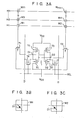
- Fig. 3A shows an arrangement of a complementary MOS (CMOS) type static memory using selective junctions Ml to Mm+l on the gate lines of transistors Tl and T2, and using control lines Hl to Hn as a diode matrix array.
- CMOS complementary MOS
- the selective junctions Ml and M2 are arranged such that with the diode D1 present on the junction M1 as shown in Fig. 3B the diode on the junction M2 is omitted and that with the diode absent on the junction M1, on the other hand, a diode Dl' as shown in Fig. C - which is similar to the diode Dl - is provided on the selective junction M2.
- the remaining selective junctions M3 and M4...Mm and Mm+1 are arranged to have the relation set out above.
- the arrangement as shown in Fig. 3A can be used as an ordinary static memory (RAM) because with the control lines Hl to Hn at the "0" level, the MOS transistors Tl and T2 are turned off as in the case of the arrangement shown in Fig. 1.
- the MOS transistor Tl With respect to the control line Hl set to "1" and the diode D1 present on the selective junction M1, for example, the MOS transistor Tl is turned on and a "0" level appears on the output terminal Ol to permit the memory cell 1 to be correspondingly set.
- the diode Dl' present on the selective junction M2 on the other hand, the MOS transistor T2 is turned on and a "0" level emerges to permit the memory cell to be correspondingly set.
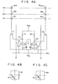
- Figs. 4A to 4C show an arrangement of an n-channel MOS type static memory. This arrangement is similar to that of Fig. 3A except for the replacement of all the transistors of Fig. 3 by N-channel MOS type transistors and the new addition of load resistors Rl and R2, and capacitances Cl and C2. The operation of Fig. 4 is similar to that of Fig. 3 with respect to function.
- Fig. 5 shows a CMOS type static memory. This arrangement is similar to that of Fig. 1 except that MOS transistors Tl' and T2'..., and Tl' and T l+1 are formed as a stacked gate structure (PROM structure).
- PROM structure stacked gate structure
- the on or the off state of the MOS transistors Tl' and T2'..., and Tl' and Tl+1 can be selected whether or not electrons are injected into an insulating film on the gate section of the MOS transistors Tl' and T2'..., and Tt' and T l+1 in the stacked gate structure. Therefore, the user can prepare the desired data items for the PROM structure which correspond in number to control lines Hl to Hn.
- Fig. 6 shows a static memory substantially similar to those shown in Figs. 2 and 4A, except for the replacement of all the MOS transistors of Fig. 5 with N-channel MOS type transistors.
- Memory contents altering data for 8 bits may be supplied from dedicated pins Pl, P2 and P3 through the corresponding output terminals to the IC memory (See Fig. 7).
- the memory contents altering data and ordinary data for 16 bits may also be supplied to the IC memory through their common input/output pins Pll, P12, P13 and P14 (See Fig. 8). That is, the arrangement shown in Fig. 8, if being equipped with the circuit of Fig. 9, permits ordinary data D from an ordinary I/O pin to be supplied under control of a R/W side and permits the memory contents altering data Hl to H16 to be supplied under control of a C/D side in Fig. 9.
- control lines HI to Hn to the corresponding memory cells See Figs. 1 to 9
- this invention should not be restricted thereto.
- only one item of data for altering the memory content may be called from one control line (for example, Hl).
- a desired number of control lines and memory contents which alter data may be provided according to the purpose for which the semiconductor memory device is used. The same thing can be applied to a semiconductor memory device for a plurality of bits.
- an improved semiconductor memory cell which can alter memory contents at any arbitrary time point of an operation.
Abstract
Description
- This invention relates to an improved semiconductor memory device which can alter, under external control, the contents of a static type random access memory (RAM), particularly, at a specific time during an operation.
- As a semiconductor memory for the conventional microcomputers etc., use is made of a specific combination of a read only memory (ROM) for storing fixed data, such as an erasable, programmable ROM (EPROM) or a mask ROM, on one hand, and a (RAM) for storing variable data, such as a static RAM or a dynamic RAM, on the other hand. The conventional nonvolatile RAM, such as an MNOS (metal nitride/oxide semiconductor) RAM, can reproduce a state corresponding to a power-off state when the power is on, but does not reproduce any mask pattern (data pattern). The conventional static RAM is in an unstable memory state upon the closure of a power source and holds given data at a data loading time. The conventional ROM is dedicated to data readout only and cannot have its memory data erased even partially for new data.
- With this situation, there is a need for a RAM that can permit the memory contents to be altered (this is not possible at the present time), to permit it to have a given memory pattern (a significant data set). There is also a need for a ROM that can permit some or all of the data to be altered (this is not possible at the present time) during the running of a program. The conventional nonvolatile RAM (MNOS type RAM) does not alter its memory contents upon the cut-off of a power source, and no consideration is given to altering its memory contents to have a given data pattern at an arbitrary time point during its use. The same things are true of the various conventional ROMs.
- With this situation, there is an urgent need for a semiconductor memory device which permits the memory contents of a RAM or a ROM to be altered, as required, at an arbitrary time during operation.
- It is accordingly the object of this invention to provide a new and improved semiconductor memory device which can alter, under external control, its memory contents at any arbitrary point of time during operation.
- According to this invention, there is provided a semiconductor memory device comprising a semiconductor memory cell for storing data, a storing data input/output means connected to the memory cell for effecting a data input/output operation with respect to the memory cell, a semiconductor switching means connected to the memory cell for altering the memory content of the memory cell, and a memory contents altering data supply means connected to the switching means for supplying memory contents altering data for switching.
- This invention can be understood by reference to the accompanying drawings in which:
- Fig. 1 is a circuit arrangement showing a semiconductor memory device according to one embodiment of this invention, the semiconductor memory device being shown as applied to a static memory;
- Figs. 2 to 6 each are circuit arrangements showing a different embodiment of this invention;
- Figs. 7 and 8 each show a detailed pin configuration for supplying data for altering the memory contents to a control line of Fig. 1; and
- Fig. 9 is a circuit arrangement showing a major part of an IC in Fig. 8.
- A semiconductor memory device according to one embodiment of this invention will be explained below by referring to Fig. 1.
- In Fig. 1, transistors Ta to Tf show metal oxide semiconductor field effect transistors MOSFETs (hereinafter referred to merely as MOS transistors) which comprise a binary logic circuit (a bistable circuit), such as a flip-flop circuit. MOS transistors Tl and T2..., and T1 and Tℓ+1 are semiconductor switching means whereby a plurality of data which is prepared to alter memory contents is selectively called to a memory cell used, for example, in a RAM. Hl... and Hn show input control lines prepared to alter the memory contents, such as to have a given data pattern, as will be described later. Ml and M2..., and Mm and Mm+1 are selective junctions between the gates of the MOS transistors on one hand and the control lines Hl...Hn on the other hand. In this connection it is to be noted that one of the selective junctions Ml and M2 is electrically connected, and the other selective junction is not electrically connected. In this way, the same connection is made up to the selective junctions Mm and Mm+1, that is, with one selective junction Mm or Mm+l electrically connected and the other selective junction not electrically connected. First memory contents altering data is prepared for the
memory cell 1 through the control line Hl. In this way, nth memory contents altering data is prepared for the corresponding memory cell through the control line Hn. D andD show data input/output lines for thememory cell 1, and SEL shows a data input/output select line for thememory cell 1. - The above-mentioned
memory cell 1 is designed for a one-power source 6-element 3-line type static memory. Here, MOS transistors Ta and Tb for loading have their drain electrodes connected to a first power source VDD, their source electrodes connected to first and second output terminals O1 and 02, respectively, and their gate electrodes connected to the second andfirst output terminals 02 and O1, respectively. The MOS transistors Tc and Td for a flip-flop circuit have their drain electrodes connected to the first and second output terminals Ol and 02, respectively, their source electrodes commonly connected to a second power source terminal VSS (normally a ground level) and their gate electrodes connected to the second andfirst output terminals 02 and Ol, respectively. The MOS transistors Te and Tf for a gate circuit have their drain electrodes connected to the data input/output linesD and D, respectively, their source electrodes connected to the first and second output terminals Ql and Q2, respectively, and their gate electrodes commonly connected to the data input/output select line SEL. - The MOS transistors Tl and T2..., and Tℓ and Tℓ+1 as switching means have those drain electrodes at the left side connected to the first output terminal O1 and those drain electrodes at the right side of Fig. 1 connected to the
second output terminal 02; their source electrodes commonly connected to the second power source terminal VSS. and their gate electrodes connected to the control lines HI..., and Hn so as to satisfy the above-mentioned requirements. - The arrangement of Fig. 1 shows a one-bit memory device, but in actual practice use is made of a multi-bit IC memory device having a plurality of
memory cells 1 corresponding to a like number of bits with the control lines HI..., and Hn similarly connected in the relation mentioned. - The operation of the semiconductor memory device as shown in Fig..1 will be explained below.
- Now suppose that the control lines HI..., and Hn are at the "0" (lower) level, that is, no memory contents altering data items are supplied to the control lines. Since the switching MOS transistors T1 and T2..., and Tℓ and Tℓ+1 are all nonconductive, the
memory cell 1 operates as an ordinary static memory. Suppose also that the memory content of thememory cell 1 is at a "0" state with the MOS transistor Td at an "ON" level and the transistor Tc at an "OFF" level in the flip-flop circuit. In order to store a level "1" into the memory cell so as to reverse the above-mentioned state, for example, a voltage going from a negative to a positive direction is applied to the data input/output line D and a negative-going voltage is applied to the data input/output select line SEL. As a result, the MOS transistors Te and Td for the gate circuit are rendered conductive with the MOS transistor Tc being on and the MOS transistor Td being off. When the data input/output select line SEL goes back to a positive voltage level, the MOS transistors Te and Td are turned off. The data input/output line D goes back to a negative voltage level. This means that a level "1" has been stored in the memory cell. - In order to read the memory content "1" out of the
memory cell 1, for example, a pulse voltage is applied on the data input/output select line SEL only. In this way, the potential on the output terminal of the flip-flop circuit, e.g., a read signal, is output.to the data input/output lines D and D. - Suppose that a plurality of
memory cells 1 is prepared to correspond to a like plurality of bits. As is well-known in the art, an X (address) decoder and Y (address) decoder, not shown, are arranged with respect to the data input/output select line SEL and data input/output lines D and D to obtain a RAM. - Let it be assumed that, for example, a "1" (high) level is supplied, as tirst data for altering the memory content, to the control line Hl during the operation of the static memory (RAM). If, in this case, the selective junction Ml is electrically connected, the MOS transistor Tl is turned on, causing a "0" level to appear on the first output terminal Ol to permit the
memory cell 1 to suffer a forced data reversal. If the selective junction M2 is electrically connected, the switching transistor T2 is turned on, causing a level "0" to appear on thesecond output terminal 02 to permit thememory cell 1 to suffer a corresponding forced data reversal. In this way, if data items are prepared with respect to the second to n-th control lines H2 to Hn, the corresponding memory cells similarly experience a corresponding data reversal to permit the memory contents to be altered. - From the above it will be appreciated that the content of the
memory cell 1, that is, that of the static memory can be altered under external control by supplying memory contents altering data at any arbitrary time point of an operation including a time immediately subsequent to the closure of the power source. Where in particular a plurality ofmemory cells 1 is prepared, the contents of the memory cells can be so altered as to have a predetermined system program or a given mask pattern (data pattern) which has been set to correspond to the respective bits. - With such a matrix array of selective junctions given as a ROM configuration, the level of the respective selective junctions in the ROM configuration is selectively read onto a corresponding one of the bit memory cells in a RAM configuration through the corresponding one of the switching MOS transistors Tl and T2...., and Tℓ and Tt+l to permit this arrangement to be used for a mask ROM. This arrangement has a combined RAM/ROM feature, thus reducing the requisite number of circuits in comparison with the case where a RAM and ROM are used separately. It is therefore possible to mount IC elements in a high packing density on a printed circuit board.
- Fig. 2 shows an arrangement of an N-channel MOS type static memory cell, which is substantially similar to that of Fig. 1 except for the use of all N-channel type MOS transistors, the use of load resistors R1 and R2 in place of the load transistors (Fig. 1) and the new addition of capacitors Cl and C2.
- Fig. 3A shows an arrangement of a complementary MOS (CMOS) type static memory using selective junctions Ml to Mm+l on the gate lines of transistors Tl and T2, and using control lines Hl to Hn as a diode matrix array. This arrangement is similar to that of Fig. 1 except for the above-mentioned matters. The selective junctions Ml and M2 are arranged such that with the diode D1 present on the junction M1 as shown in Fig. 3B the diode on the junction M2 is omitted and that with the diode absent on the junction M1, on the other hand, a diode Dl' as shown in Fig. C - which is similar to the diode Dl - is provided on the selective junction M2. In this way, the remaining selective junctions M3 and M4...Mm and Mm+1 are arranged to have the relation set out above.
- The arrangement as shown in Fig. 3A can be used as an ordinary static memory (RAM) because with the control lines Hl to Hn at the "0" level, the MOS transistors Tl and T2 are turned off as in the case of the arrangement shown in Fig. 1. With respect to the control line Hl set to "1" and the diode D1 present on the selective junction M1, for example, the MOS transistor Tl is turned on and a "0" level appears on the output terminal Ol to permit the
memory cell 1 to be correspondingly set. With the diode Dl' present on the selective junction M2, on the other hand, the MOS transistor T2 is turned on and a "0" level emerges to permit the memory cell to be correspondingly set. - Figs. 4A to 4C show an arrangement of an n-channel MOS type static memory. This arrangement is similar to that of Fig. 3A except for the replacement of all the transistors of Fig. 3 by N-channel MOS type transistors and the new addition of load resistors Rl and R2, and capacitances Cl and C2. The operation of Fig. 4 is similar to that of Fig. 3 with respect to function.
- Fig. 5 shows a CMOS type static memory. This arrangement is similar to that of Fig. 1 except that MOS transistors Tl' and T2'..., and Tℓ' and Tℓ+1 are formed as a stacked gate structure (PROM structure). In this arrangement, the on or the off state of the MOS transistors Tl' and T2'..., and Tℓ' and Tℓ+1 can be selected whether or not electrons are injected into an insulating film on the gate section of the MOS transistors Tl' and T2'..., and Tt' and Tℓ+1 in the stacked gate structure. Therefore, the user can prepare the desired data items for the PROM structure which correspond in number to control lines Hl to Hn.
- Fig. 6 shows a static memory substantially similar to those shown in Figs. 2 and 4A, except for the replacement of all the MOS transistors of Fig. 5 with N-channel MOS type transistors.
- Memory contents altering data for 8 bits may be supplied from dedicated pins Pl, P2 and P3 through the corresponding output terminals to the IC memory (See Fig. 7). The memory contents altering data and ordinary data for 16 bits may also be supplied to the IC memory through their common input/output pins Pll, P12, P13 and P14 (See Fig. 8). That is, the arrangement shown in Fig. 8, if being equipped with the circuit of Fig. 9, permits ordinary data D from an ordinary I/O pin to be supplied under control of a R/W side and permits the memory contents altering data Hl to H16 to be supplied under control of a C/D side in Fig. 9.
- Although the memory contents altering data items have been explained as being selectively called from the corresponding control lines HI to Hn to the corresponding memory cells (See Figs. 1 to 9), this invention should not be restricted thereto. Alternatively, only one item of data for altering the memory content may be called from one control line (for example, Hl). A desired number of control lines and memory contents which alter data may be provided according to the purpose for which the semiconductor memory device is used. The same thing can be applied to a semiconductor memory device for a plurality of bits.
- This invention should not be restricted to the above-mentioned embodiments. Various changes or modifications may be made without departing from the spirit and scope of this invention.
- As evident from the above, according to this invention an improved semiconductor memory cell is provided which can alter memory contents at any arbitrary time point of an operation.
Claims (7)
Applications Claiming Priority (2)
| Application Number | Priority Date | Filing Date | Title |
|---|---|---|---|
| JP193747/83 | 1983-10-17 | ||
| JP58193747A JPS6085496A (en) | 1983-10-17 | 1983-10-17 | Semiconductor memory |
Publications (3)
| Publication Number | Publication Date |
|---|---|
| EP0140235A2 true EP0140235A2 (en) | 1985-05-08 |
| EP0140235A3 EP0140235A3 (en) | 1986-10-29 |
| EP0140235B1 EP0140235B1 (en) | 1989-08-16 |
Family
ID=16313135
Family Applications (1)
| Application Number | Title | Priority Date | Filing Date |
|---|---|---|---|
| EP19840112160 Expired EP0140235B1 (en) | 1983-10-17 | 1984-10-10 | Semiconductor memory device |
Country Status (3)
| Country | Link |
|---|---|
| EP (1) | EP0140235B1 (en) |
| JP (1) | JPS6085496A (en) |
| DE (1) | DE3479461D1 (en) |
Cited By (3)
| Publication number | Priority date | Publication date | Assignee | Title |
|---|---|---|---|---|
| EP0430101A2 (en) * | 1989-11-24 | 1991-06-05 | Nec Corporation | Semiconductor memory device having resettable memory cells |
| US5179538A (en) * | 1989-06-30 | 1993-01-12 | The Boeing Company | Memory system including CMOS memory cells and bipolar sensing circuit |
| US6639825B2 (en) | 1999-12-14 | 2003-10-28 | Infineon Technologies Ag | Data memory |
Families Citing this family (2)
| Publication number | Priority date | Publication date | Assignee | Title |
|---|---|---|---|---|
| JPS61230698A (en) * | 1985-04-05 | 1986-10-14 | Nec Corp | Random access semiconductor memory cell |
| ES2584527T3 (en) * | 2008-04-17 | 2016-09-28 | Intrinsic Id B.V. | Method to reduce the appearance of burning due to temperature instability in negative polarization |
Citations (5)
| Publication number | Priority date | Publication date | Assignee | Title |
|---|---|---|---|---|
| US3798621A (en) * | 1971-12-30 | 1974-03-19 | Ibm | Monolithic storage arrangement with latent bit pattern |
| DE2711221A1 (en) * | 1976-03-15 | 1977-09-29 | Tokyo Shibaura Electric Co | ENERGY INDEPENDENT STORAGE DEVICE |
| US4104719A (en) * | 1976-05-20 | 1978-08-01 | The United States Of America As Represented By The Secretary Of The Navy | Multi-access memory module for data processing systems |
| US4193128A (en) * | 1978-05-31 | 1980-03-11 | Westinghouse Electric Corp. | High-density memory with non-volatile storage array |
| US4347585A (en) * | 1980-06-09 | 1982-08-31 | International Business Machines Corporation | Reproduce only storage matrix |
-
1983
- 1983-10-17 JP JP58193747A patent/JPS6085496A/en active Pending
-
1984
- 1984-10-10 DE DE8484112160T patent/DE3479461D1/en not_active Expired
- 1984-10-10 EP EP19840112160 patent/EP0140235B1/en not_active Expired
Patent Citations (5)
| Publication number | Priority date | Publication date | Assignee | Title |
|---|---|---|---|---|
| US3798621A (en) * | 1971-12-30 | 1974-03-19 | Ibm | Monolithic storage arrangement with latent bit pattern |
| DE2711221A1 (en) * | 1976-03-15 | 1977-09-29 | Tokyo Shibaura Electric Co | ENERGY INDEPENDENT STORAGE DEVICE |
| US4104719A (en) * | 1976-05-20 | 1978-08-01 | The United States Of America As Represented By The Secretary Of The Navy | Multi-access memory module for data processing systems |
| US4193128A (en) * | 1978-05-31 | 1980-03-11 | Westinghouse Electric Corp. | High-density memory with non-volatile storage array |
| US4347585A (en) * | 1980-06-09 | 1982-08-31 | International Business Machines Corporation | Reproduce only storage matrix |
Non-Patent Citations (2)
| Title |
|---|
| IBM TECHNICAL DISCLOSURE BULLETIN, vol. 23, no. 4, September 1980, pages 1373-1374, New York, US; R.J. PRILIK: "Shared random-access memory and ROS functions by modified random-access memory design" * |
| INTEL MARKETING COMMUNICATIONS, "The semiconductor memory book" 1978, pages 294-300, John Wiley & Sons, New York, US; B.GREENE: "Designing with 2708 EPROM" * |
Cited By (5)
| Publication number | Priority date | Publication date | Assignee | Title |
|---|---|---|---|---|
| US5179538A (en) * | 1989-06-30 | 1993-01-12 | The Boeing Company | Memory system including CMOS memory cells and bipolar sensing circuit |
| EP0430101A2 (en) * | 1989-11-24 | 1991-06-05 | Nec Corporation | Semiconductor memory device having resettable memory cells |
| EP0430101A3 (en) * | 1989-11-24 | 1992-06-17 | Nec Corporation | Semiconductor memory device having resettable memory cells |
| US5285420A (en) * | 1989-11-24 | 1994-02-08 | Nec Corporation | Semiconductor memory device having concurrently resettable memory cells |
| US6639825B2 (en) | 1999-12-14 | 2003-10-28 | Infineon Technologies Ag | Data memory |
Also Published As
| Publication number | Publication date |
|---|---|
| EP0140235B1 (en) | 1989-08-16 |
| EP0140235A3 (en) | 1986-10-29 |
| DE3479461D1 (en) | 1989-09-21 |
| JPS6085496A (en) | 1985-05-14 |
Similar Documents
| Publication | Publication Date | Title |
|---|---|---|
| US4271487A (en) | Static volatile/non-volatile ram cell | |
| US4546273A (en) | Dynamic re-programmable PLA | |
| US5097152A (en) | Buffer circuit used in a semiconductor device operating by different supply potentials and method of operating the same | |
| US5111079A (en) | Power reduction circuit for programmable logic device | |
| EP0182595B1 (en) | Semiconductor nonvolatile memory device | |
| US4342101A (en) | Nonvolatile semiconductor memory circuits | |
| EP0347530A2 (en) | Static random access memory device with a power dissipation reduction function | |
| US3703710A (en) | Semiconductor memory | |
| US4733371A (en) | Semiconductor memory device with high voltage switch | |
| US4275312A (en) | MOS decoder logic circuit having reduced power consumption | |
| EP0171718B1 (en) | Decoder circuit in an ic memory chip | |
| US4508977A (en) | Re-programmable PLA | |
| US4174541A (en) | Bipolar monolithic integrated circuit memory with standby power enable | |
| JPS63179617A (en) | Voltage switching circuit to which mos technology is applied | |
| US5818758A (en) | Zero voltage drop negative switch for dual well processes | |
| US5280451A (en) | Signature circuit for non-volatile memory device | |
| US4000429A (en) | Semiconductor circuit device | |
| US4864541A (en) | Integrated circuit of the logic circuit type comprising an electrically programmable non-volatile memory | |
| US4641285A (en) | Line change-over circuit and semiconductor memory using the same | |
| EP0140235A2 (en) | Semiconductor memory device | |
| US4910710A (en) | Input circuit incorporated in a semiconductor device | |
| US4694431A (en) | Semiconductor memory device with increased adaptability | |
| US4860258A (en) | Electrically programmable non-volatile memory having sequentially deactivated write circuits | |
| EP0107355A2 (en) | CMIS circuit device | |
| US4610003A (en) | Dynamic type semiconductor memory device |
Legal Events
| Date | Code | Title | Description |
|---|---|---|---|
| PUAI | Public reference made under article 153(3) epc to a published international application that has entered the european phase |
Free format text: ORIGINAL CODE: 0009012 |
|
| 17P | Request for examination filed |
Effective date: 19841107 |
|
| AK | Designated contracting states |
Designated state(s): DE FR GB |
|
| PUAL | Search report despatched |
Free format text: ORIGINAL CODE: 0009013 |
|
| AK | Designated contracting states |
Kind code of ref document: A3 Designated state(s): DE FR GB |
|
| 17Q | First examination report despatched |
Effective date: 19870326 |
|
| GRAA | (expected) grant |
Free format text: ORIGINAL CODE: 0009210 |
|
| AK | Designated contracting states |
Kind code of ref document: B1 Designated state(s): DE FR GB |
|
| REF | Corresponds to: |
Ref document number: 3479461 Country of ref document: DE Date of ref document: 19890921 |
|
| ET | Fr: translation filed | ||
| PLBE | No opposition filed within time limit |
Free format text: ORIGINAL CODE: 0009261 |
|
| STAA | Information on the status of an ep patent application or granted ep patent |
Free format text: STATUS: NO OPPOSITION FILED WITHIN TIME LIMIT |
|
| 26N | No opposition filed | ||
| PGFP | Annual fee paid to national office [announced via postgrant information from national office to epo] |
Ref country code: GB Payment date: 19971001 Year of fee payment: 14 |
|
| PGFP | Annual fee paid to national office [announced via postgrant information from national office to epo] |
Ref country code: FR Payment date: 19971009 Year of fee payment: 14 |
|
| PGFP | Annual fee paid to national office [announced via postgrant information from national office to epo] |
Ref country code: DE Payment date: 19971017 Year of fee payment: 14 |
|
| PG25 | Lapsed in a contracting state [announced via postgrant information from national office to epo] |
Ref country code: GB Free format text: LAPSE BECAUSE OF NON-PAYMENT OF DUE FEES Effective date: 19981010 |
|
| GBPC | Gb: european patent ceased through non-payment of renewal fee |
Effective date: 19981010 |
|
| PG25 | Lapsed in a contracting state [announced via postgrant information from national office to epo] |
Ref country code: FR Free format text: LAPSE BECAUSE OF NON-PAYMENT OF DUE FEES Effective date: 19990630 |
|
| REG | Reference to a national code |
Ref country code: FR Ref legal event code: ST |
|
| PG25 | Lapsed in a contracting state [announced via postgrant information from national office to epo] |
Ref country code: DE Free format text: LAPSE BECAUSE OF NON-PAYMENT OF DUE FEES Effective date: 19990803 |