EP0140149B1 - Power conversion device for solar cell - Google Patents
Power conversion device for solar cell Download PDFInfo
- Publication number
- EP0140149B1 EP0140149B1 EP84111325A EP84111325A EP0140149B1 EP 0140149 B1 EP0140149 B1 EP 0140149B1 EP 84111325 A EP84111325 A EP 84111325A EP 84111325 A EP84111325 A EP 84111325A EP 0140149 B1 EP0140149 B1 EP 0140149B1
- Authority
- EP
- European Patent Office
- Prior art keywords
- solar cell
- frequency
- output
- electrical power
- power source
- Prior art date
- Legal status (The legal status is an assumption and is not a legal conclusion. Google has not performed a legal analysis and makes no representation as to the accuracy of the status listed.)
- Expired - Lifetime
Links
- 238000006243 chemical reaction Methods 0.000 title claims description 10
- 230000007423 decrease Effects 0.000 claims description 10
- 230000001360 synchronised effect Effects 0.000 claims description 3
- 230000008878 coupling Effects 0.000 claims 1
- 238000010168 coupling process Methods 0.000 claims 1
- 238000005859 coupling reaction Methods 0.000 claims 1
- 238000004804 winding Methods 0.000 description 39
- 239000003990 capacitor Substances 0.000 description 19
- 238000010586 diagram Methods 0.000 description 13
- 230000002441 reversible effect Effects 0.000 description 8
- 229920006395 saturated elastomer Polymers 0.000 description 7
- 230000004907 flux Effects 0.000 description 6
- 230000010355 oscillation Effects 0.000 description 6
- 230000000694 effects Effects 0.000 description 4
- 230000001965 increasing effect Effects 0.000 description 4
- 230000000717 retained effect Effects 0.000 description 4
- 230000006870 function Effects 0.000 description 3
- 238000012423 maintenance Methods 0.000 description 3
- 230000003247 decreasing effect Effects 0.000 description 2
- 238000011161 development Methods 0.000 description 2
- MYMOFIZGZYHOMD-UHFFFAOYSA-N Dioxygen Chemical compound O=O MYMOFIZGZYHOMD-UHFFFAOYSA-N 0.000 description 1
- UFHFLCQGNIYNRP-UHFFFAOYSA-N Hydrogen Chemical compound [H][H] UFHFLCQGNIYNRP-UHFFFAOYSA-N 0.000 description 1
- 238000013459 approach Methods 0.000 description 1
- 238000010276 construction Methods 0.000 description 1
- 230000002950 deficient Effects 0.000 description 1
- 229910001882 dioxygen Inorganic materials 0.000 description 1
- 239000003792 electrolyte Substances 0.000 description 1
- 238000002474 experimental method Methods 0.000 description 1
- 238000010348 incorporation Methods 0.000 description 1
- 230000001939 inductive effect Effects 0.000 description 1
- 239000013589 supplement Substances 0.000 description 1
Images

Classifications
-
- H—ELECTRICITY
- H02—GENERATION; CONVERSION OR DISTRIBUTION OF ELECTRIC POWER
- H02M—APPARATUS FOR CONVERSION BETWEEN AC AND AC, BETWEEN AC AND DC, OR BETWEEN DC AND DC, AND FOR USE WITH MAINS OR SIMILAR POWER SUPPLY SYSTEMS; CONVERSION OF DC OR AC INPUT POWER INTO SURGE OUTPUT POWER; CONTROL OR REGULATION THEREOF
- H02M7/00—Conversion of AC power input into DC power output; Conversion of DC power input into AC power output
- H02M7/42—Conversion of DC power input into AC power output without possibility of reversal
- H02M7/44—Conversion of DC power input into AC power output without possibility of reversal by static converters
- H02M7/48—Conversion of DC power input into AC power output without possibility of reversal by static converters using discharge tubes with control electrode or semiconductor devices with control electrode
- H02M7/53—Conversion of DC power input into AC power output without possibility of reversal by static converters using discharge tubes with control electrode or semiconductor devices with control electrode using devices of a triode or transistor type requiring continuous application of a control signal
- H02M7/537—Conversion of DC power input into AC power output without possibility of reversal by static converters using discharge tubes with control electrode or semiconductor devices with control electrode using devices of a triode or transistor type requiring continuous application of a control signal using semiconductor devices only, e.g. single switched pulse inverters
- H02M7/538—Conversion of DC power input into AC power output without possibility of reversal by static converters using discharge tubes with control electrode or semiconductor devices with control electrode using devices of a triode or transistor type requiring continuous application of a control signal using semiconductor devices only, e.g. single switched pulse inverters in a push-pull configuration
- H02M7/53803—Conversion of DC power input into AC power output without possibility of reversal by static converters using discharge tubes with control electrode or semiconductor devices with control electrode using devices of a triode or transistor type requiring continuous application of a control signal using semiconductor devices only, e.g. single switched pulse inverters in a push-pull configuration with automatic control of output voltage or current
- H02M7/53806—Conversion of DC power input into AC power output without possibility of reversal by static converters using discharge tubes with control electrode or semiconductor devices with control electrode using devices of a triode or transistor type requiring continuous application of a control signal using semiconductor devices only, e.g. single switched pulse inverters in a push-pull configuration with automatic control of output voltage or current in a push-pull configuration of the parallel type
-
- G—PHYSICS
- G05—CONTROLLING; REGULATING
- G05F—SYSTEMS FOR REGULATING ELECTRIC OR MAGNETIC VARIABLES
- G05F1/00—Automatic systems in which deviations of an electric quantity from one or more predetermined values are detected at the output of the system and fed back to a device within the system to restore the detected quantity to its predetermined value or values, i.e. retroactive systems
- G05F1/66—Regulating electric power
- G05F1/67—Regulating electric power to the maximum power available from a generator, e.g. from solar cell
-
- Y—GENERAL TAGGING OF NEW TECHNOLOGICAL DEVELOPMENTS; GENERAL TAGGING OF CROSS-SECTIONAL TECHNOLOGIES SPANNING OVER SEVERAL SECTIONS OF THE IPC; TECHNICAL SUBJECTS COVERED BY FORMER USPC CROSS-REFERENCE ART COLLECTIONS [XRACs] AND DIGESTS
- Y02—TECHNOLOGIES OR APPLICATIONS FOR MITIGATION OR ADAPTATION AGAINST CLIMATE CHANGE
- Y02E—REDUCTION OF GREENHOUSE GAS [GHG] EMISSIONS, RELATED TO ENERGY GENERATION, TRANSMISSION OR DISTRIBUTION
- Y02E10/00—Energy generation through renewable energy sources
- Y02E10/50—Photovoltaic [PV] energy
- Y02E10/56—Power conversion systems, e.g. maximum power point trackers
-
- Y—GENERAL TAGGING OF NEW TECHNOLOGICAL DEVELOPMENTS; GENERAL TAGGING OF CROSS-SECTIONAL TECHNOLOGIES SPANNING OVER SEVERAL SECTIONS OF THE IPC; TECHNICAL SUBJECTS COVERED BY FORMER USPC CROSS-REFERENCE ART COLLECTIONS [XRACs] AND DIGESTS
- Y10—TECHNICAL SUBJECTS COVERED BY FORMER USPC
- Y10S—TECHNICAL SUBJECTS COVERED BY FORMER USPC CROSS-REFERENCE ART COLLECTIONS [XRACs] AND DIGESTS
- Y10S136/00—Batteries: thermoelectric and photoelectric
- Y10S136/291—Applications
- Y10S136/293—Circuits
-
- Y—GENERAL TAGGING OF NEW TECHNOLOGICAL DEVELOPMENTS; GENERAL TAGGING OF CROSS-SECTIONAL TECHNOLOGIES SPANNING OVER SEVERAL SECTIONS OF THE IPC; TECHNICAL SUBJECTS COVERED BY FORMER USPC CROSS-REFERENCE ART COLLECTIONS [XRACs] AND DIGESTS
- Y10—TECHNICAL SUBJECTS COVERED BY FORMER USPC
- Y10S—TECHNICAL SUBJECTS COVERED BY FORMER USPC CROSS-REFERENCE ART COLLECTIONS [XRACs] AND DIGESTS
- Y10S323/00—Electricity: power supply or regulation systems
- Y10S323/906—Solar cell systems
Definitions
- This invention relates to a power conversion device for a solar cell. More particularly, this invention relates to a power conversion device for a solar cell which can draw from the solar cell the maximum electric power corresponding to the amount of sunlight impinging upon the solar cell and can establish interconnection between the solar cell and a commercial ac power source.
- Solar cells as widely known are designed to absorb sunlight and generate electric current.
- the generated electric current or electric power therefore, varies with the varying amount of sunlight impinging upon the solar cell.
- no electric power can be drawn from the solar cell.
- the lead battery which has found popular use when adopted as the secondary battery, it not merely entails the danger due to the generation of hydrogen gas and oxygen gas but also necessitates maintenance such as replenishment of electrolyte.
- the lead battery therefore, has a disadvantage that it cannot be utilized in such a small power system as owned by any household power consumer.
- the solar cell system is desired to be capable of connection to the commercial power source.
- An object of this invention is to provide a power conversion device of simple configuration for a solar cell which permits the solar cell to be connected to the commercial power source and enables the maximum electric power corresponding to the amount of incident sunlight to be drawn from the solar cell.
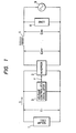
- Fig. 1 is a block diagram of one embodiment of this invention.
- a solar cell 1 supplies electric power corresponding to the amount of incident sunlight to an inverter 2.
- a voltage controlled oscillator (VCO) 3 oscillates with a frequency f corresponding to the output voltage Ei of the solar cell 1.
- the aforementioned inverter 2 operates with the aforementioned frequency f and converts the direct current from the solar cell 1 into an alternating current.
- the aforementioned frequency f of the oscillation increases in proportion as the magnitude of the output voltage Ei increases.
- the output (ac) side of the inverter 2 is connected via an inductor 4 to a commercial ac power source 5.
- a load 6 is connected to the output side of the inverter 2 or to the commercial ac power source 5.
- the current li generated by the solar cell 1 is supplied to the inverter 2 and the voltage controlled oscillator 3.
- the terminal voltage of the solar cell 1 is Ei.
- the voltage controlled oscillator 3 generates oscillation with the frequency f and, as the result, the inverter 2 generates an alternating current voltage Einv with the aforementioned frequency f.
- Einv denotes the effective value of fundamental frequency component.
- phase of the ac voltage Einv of the inverter 2 is in advance of that of the ac waveform Eac of the commercial power source 5, the power flows from the inverter 2 side via the inductor 4 to the commercial power source 5 side, effecting power supply from the solar cell 1 to the load 6.
- the output frequency of the inverter 2 is automatically synchronized with the frequency of the commercial power source 5. Now, the principle underlying this automatic synchronization will be described below.
- the voltage controlled oscillator 3 is caused to generate oscillation with the frequency f and the inverter 2 to generate the ac voltage Einv with the fundamental frequency f. It is further assumed that the phase of the output ac voltage Einv of the inverter 2 is in advance of that of the commercial power source 5 and, as the result, the power is flowing from the solar cell 1 side via the inductor 4 to the commercial power source side 5.
- the oscillation frequency f of the voltage controlled oscillator 3 tends to increase proportionally.
- the frequency of the output ac of the inverter 2 tends to increase and the phase of the output ac voltage thereof tends to advance, namely the advanced phase angle of the output ac voltage Einv of the inverter 2 relative to the voltage Eac of the commercial power source 5 tends to increase.
- the voltage drop due to the internal resistance of the solar cell 1 decreased effectively to increase the output voltage Ei of the solar cell 1.
- a decrease of the output voltage Ei of the solar cell 1 and the falling ac frequency of the inverter 2 are effectively non-linear.
- the frequency of the output ac voltage Einv of the inverter 2 is automatically retained at a fixed value and synchronized with the frequency of the commercial power source 5 in spite of variation in the amount of incident sunlight reaching the solar cell.
- Fig. 2 shows the relation between the terminal voltage in V (horizontal axis) and the output power in mW (vertical axis) of the solar cell 1, with the amount of incident sunlight or the solar energy in mW/cm 2 as the parameter. It is noted from this graph that the power which can be drawn from the solar cell 1 is naturally increased by the increase of the incident solar energy and is also varied by the terminal voltage.
- the output power increases in proportion as the terminal voltage increases but the output power conversely decreases when the terminal voltage surpasses a certain value.
- this optimum terminal voltage is substantially constant (in the neighborhood of 4 volts) as noted from Fig. 2.
- the maximum power corresponding to the existing amount of incident sunlight can be drawn at all times from the solar cell 1 when the circuit constants of the various parts are selected so as to equalize the output voltage Ei of the solar cell 1 with the aforementioned optimum terminal voltage.
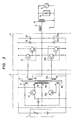
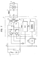
- Fig. 3 is a diagram illustrating a typical circuit of another embodiment of the present invention.
- the same numerical symbols as those of Fig. 1 denote identical or equal component parts of the device.
- primary windings 8, 8a, secondary windings 9,9a, and output windings 10, 10a are coiled.
- the center terminals of the primary windings 8,8a are joined mutually and connected to the positive terminal of the solar cell 1.
- the remaining terminals are connected to the collectors of the corresponding transistors 12,12a.
- the emitters of the aforementioned transistors 12, 12a are joined mutually and connected to the negative terminal of the solar cell 1.
- the bases of the aforementioned transistors 12, 12a are respectively connected to the terminals of the secondary windings 9, 9a.
- the remaining terminals of the secondary windings 9, 9a are mutually joined through their respective series- connected resistors and connected through another resistor to the positive terminal of the solar cell 1.
- the primary windings 8, 8a, secondary windings 9,9a, output windings 10, 10a, transistors 12, 12a, etc. described above make up a well-known Royer's oscillator circuit, which functions in this embodiment as a voltage controlled oscillator 3.
- Capacitors 23, 23a are serially connected between the positive and negative terminals of the solar cell 1.
- Diodes 24, 24a are serially connected in a reversely polarized manner between the positive and negative terminals of the solar cell 1.
- Transistors 21, 21 a are each formed of a Darling- ton transistor and are connected in reverse parallelism to the aforementioned diodes 24, 24a.
- the bases and emitters of the aforementioned transistors 21, 21 a are respectively connected to the opposite terminals of the output windings 10, 10a.
- the node of the aforementioned diodes 24, 24a is connected via the inductor 4 to one of the input terminals of the output transformer 16.
- the node of the aforementioned capacitors 23, 23a is connected to the other input terminal of the aforementioned output transformer 16 and one terminal of the commercial power source 5.
- the other terminal of the commercial power source 5 is connected to the output terminal of the output transformer 16.
- the transistors 21, 21a, capacitors 23, 23a and diodes 24, 24a mentioned above make up a half bridge inverter 2.
- either of the transistors 12,12a is turned on.
- a primary current flows through a circuit of solar cell 1 primary winding 8 - transistor 12 ⁇ solar cell 1, inducing a voltage in the secondary windings 9,9a.
- the voltage of the secondary winding 9 confers a forward bias upon the transistor 12 and the voltage of the secondary winding 9a confers a reverse bias upon the transistor 12a. As the result, there is generated a so-called positive feedback action, which induces abrupt saturation of the transistor 12.
- the core 7 is excited by the current flowing through the primary winding.
- the voltage of the secondary winding 9 is extinguished and the positive bias of the base current of the transistor 12 is lowered to 0, with the result that the transistor 12 is shut off.
- the magnetic flux of the core begins to decrease.
- a voltage of reversed polarity is induced in the secondary windings 9,9a and a forward bias is applied to the transistor 12a.
- a primary current flows through a circuit of solar cell 1 ⁇ primary winding 8a ⁇ transistor 12a solar cell 1.
- the transistor 12a is saturated in due course of time and the core 7 is excited so that the magnetic flux of the core 7 is saturated in the reverse direction.
- the transistors 21, 21a alternately assume the status of forward bias.
- the capacitors 23, 23a are charged by means of the solar cell 1.
- the transistor 21 is turned on, therefore, the charge of the capacitor 23 is released through a path of capacitor 23 ⁇ transistor 21 ⁇ inductor 4 ⁇ output transformer 16-j capacitor 23.
- the rate of saturation of the transistors 12, 12a and that of the saturable core 7 in the voltage controlled oscillator 3 depend on the voltage of the solar cell 1. In other words, the saturation rates increase with the increasing magnitude of the voltage of the solar cell 1.
- the Royer's oscillator satisfactorily fulfils its function as the voltage controlled oscillator 3. The same operation and effect as described with reference to Fig. 1 can be attained by the circuit of Fig. 3.
- Fig. 4 is a graph of the data obtained in an operation of the embodiment of Fig. 3, except that a power source unit formed by series connection of a battery of 64V and a variable resistor as internal resistance to serve as a model simulating the solar cell 1. Specifically, the graph shows the variations of output voltage (Ei), output power (P), and conversion efficiency ( ⁇ ) as caused by varying the internal resistance and consequently the output current li in the model.
- the inductance of the inductor 4 is fixed at 30 mH and the voltage of the commercial power source 5 and the output ac voltage of the inverter 2 are fixed at 27 V.
- theterminal voltage is retained substantially constant at 60 V and the conversion efficiency is as high as about 90%.
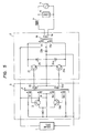
- Fig. 5 is a diagram of a typical circuit of another embodiment of this invention.
- the same numerical signs as those found in Fig. 3 denote identical or equal component parts.
- the terminals of the output windings 10, 10a are mutually joined and the remaining terminals thereof are connected to the bases of the transistors 21, 21a.
- the common node of the aforementioned output windings 10, 10a is connected to the emitters of the transistors 21, 21a and to the negative terminal of the solar cell 1 and one of the terminals of the capacitor 23c.
- the diodes 24, 24a are connected in reverse polarity.
- the collectors of the transistors 21, 21a are connected respectively to the terminals of the primary windings 17, 17a of the output transformer 16.
- the remaining terminals of the primary windings 17, 17a of the aforementioned output transformer 16 are mutually joined and the node is connected to the positive terminal of the solar cell 1 and the remaining terminal of the capacitor 23c.
- the secondary winding 18 of the output transformer 16 is connected via the inductor 4 to the commercial power source 5.
- the transistors 21 and 21a are alternately turned on in much the same manner as in the embodiment of Fig. 3.
- an alternating current is generated in a secondary winding 18 and is fed via the inductor 4 to the load 6 and the commercial power source 5.
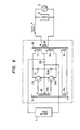
- Fig. 6 is a diagram of a typical circuit of yet another embodiment of the present invention.
- the same numerical signs as those found in Fig. 5 denote identical or equal component parts.
- the transistor 21 If the transistor 21 is turned on, the current from the solar cell 1 and the discharge current by the charge accumulated in the capacitor 23c are caused to flow through the primary winding 17 and the transistor 21.
- the voltage induced in the tertiary winding 19 is applied to the feedback winding 19a.
- the voltages induced in the output windings 10, 10a by the feedback winding 19a give a forward bias upon the transistor 21 and a reverse bias upon the transistor 21a.
- the voltage of the output winding 10 is extinguished and the base current of the transistor 21 is reduced to 0, with the result that the transistor 21 is shut off. Since the magnetic flux of the saturable core 7 consequently begins to decrease, a voltage of reverse polarity is induced in the output windings 10, 10a.
- the transistor 21a assumes a forward bias and the transistor 21 a reverse bias.
- the transistor 21 a is turned on to start flow of the current from the primary winding 17a through the transistor 21 a.
- the transistor 21a a is saturated in this time and the saturable core 7 is excited so that the magnetic flux of the core 7 is saturated in a reverse direction.
- the two transistors 21 and 21 a are alternately turned on, with the result that a primary current is supplied to the primary windings 17, 17a and an alternating current (rectangular waveform) is generated in the secondary winding 18.
- This alternating current is filtered by the inductor 4 and supplied to the commercial power source 5 and to the load 6.
- the foregoing embodiments have been invariably described on the assumption that the operating frequency of the inverter, namely the output frequency f of the voltage controlled oscillator 3, is substantially equal to the fundamental frequency of the ac output of the inverter 2 or the frequency of the commercial power source 5.
- a PWM (pulse width modulation) inverter may be used as the inverter 2 of this invention.
- Fig. 7 is a block diagram of yet another embodiment of this invention involving the use of a PWM inverter.
- the same numerical symbols as those of Fig. 5 denote identical or equal component parts.
- the voltage controlled oscillator 3A generates oscillation with a frequency which is an integral multiple of the frequency of the commercial power source 5.
- An address counter 32 serves to take count of the output pulses of the voltage controlled oscillator 3A and gives the counted value as an address signal to a ROM (read only memory) 34.
- the ROM 34 issues the output of "1" or "0” corresponding to the sine wave in accordance with the aforementioned address signal. By the aforementioned output "1” or "0”, one of the transistors 21, 21a is turned ON and the other transistor OFF respectively. In this configuration, the inverter output Einv to be obtained is free from higher harmonics.
- the present invention has been described as used in the form of a power source for an ac load.
- this invention can be applied to a dc load.
- the given dc load may, for example, be connected directly to the solar cell 1.
- the excess power is transmitted to the commercial power source 5 side as described above.
- the supplement of dc current is fed from the commercial power source 5 via the inverter 2 to the dc load because the inverter 2 functions as a rectifier (or ac-to-dc converter). Consequently, the terminal voltage of the solar cell 1 is retained substantially constant.
Landscapes
- Engineering & Computer Science (AREA)
- Power Engineering (AREA)
- Life Sciences & Earth Sciences (AREA)
- Sustainable Development (AREA)
- Sustainable Energy (AREA)
- Physics & Mathematics (AREA)
- Electromagnetism (AREA)
- General Physics & Mathematics (AREA)
- Radar, Positioning & Navigation (AREA)
- Automation & Control Theory (AREA)
- Inverter Devices (AREA)
- Control Of Electrical Variables (AREA)
Description
- This invention relates to a power conversion device for a solar cell. More particularly, this invention relates to a power conversion device for a solar cell which can draw from the solar cell the maximum electric power corresponding to the amount of sunlight impinging upon the solar cell and can establish interconnection between the solar cell and a commercial ac power source.
- Solar cells, as widely known are designed to absorb sunlight and generate electric current. The generated electric current or electric power, therefore, varies with the varying amount of sunlight impinging upon the solar cell. During the night, no electric power can be drawn from the solar cell.
- In the solar cell power source systems, which have been reduced to practical utility, therefore, it is customary that they are combined with secondary batteries to form so-called floating charging circuits. In this construction, since the secondary batteries are charged during the daytime generally abundant with sunlight, necessary electric power can be drawn from them even during the night or on rainy or cloudy days deficient in sunlight.
- In the conventional system, when the lead battery which has found popular use is adopted as the secondary battery, it not merely entails the danger due to the generation of hydrogen gas and oxygen gas but also necessitates maintenance such as replenishment of electrolyte. The lead battery, therefore, has a disadvantage that it cannot be utilized in such a small power system as owned by any household power consumer.
- Storage batteries of other types are expensive and possess no ample capacity.
- Further, since the commercial power source (100/200 V, 50/60 cycles) is widely used for various kinds of devices or equipments, the solar cell system is desired to be capable of connection to the commercial power source.
- This interconnection, however, provides disadvantageous in respect that it necessitates additional incorporation of an inverter, for example, and inevitably complicates the mechanism, increases the size, and adds to the cost of equipment.
- C. Franx 'A New Approach to Solar Pump Systems Using Submersible Motors" Photovoltaic Solar Energy Conference, Berlin, W. Germany, Apr. 23-26, 1979, pp. 1038-1046, discloses a pump system consisting of solar modules feeding a pump via a DC-AC convertor. The convertor provides power match between the solar panels and the pump under varying conditions of power supply or power demand. The power match is controlled by varying the frequency, which is on its turn enabled by the application of the pulse width modulation (PWM) principle. This state of art, however, does not disclose the possibility of connecting the convertor output with a commercial power source.
- This invention has been'produced with a view to eliminating the drawbacks mentioned above. An object of this invention, therefore, is to provide a power conversion device of simple configuration for a solar cell which permits the solar cell to be connected to the commercial power source and enables the maximum electric power corresponding to the amount of incident sunlight to be drawn from the solar cell.
- Starting, from the prior art described in the Franx-article, this object is reached by the features of
claim 1. -
- Fig. 1 is a block diagram illustrating one embodiment of the present invention.
- Fig. 2 is a graph showing the relation between the terminal voltage in V (horizontal axis) and the output power in mW (vertical axis) of the solar cell with the amount of incident sunlight (incident solar energy) in mW/cm2 as the parameter.
- Fig. 3 is a diagram illustrating a typical circuit of another embodiment of this invention.
- Fig. 4 is a graph showing the variations of the output voltage (Ei), output power (P) and the convertion efficiency (n) caused by varying the internal resistance of the solar cell and consequently the output electric current (li).
- Fig. 5 and Fig. 6 are typical circuit diagrams of other embodiments of this invention.
- Fig. 7 is a block diagram of yet another embodiment of this invention involving the use of a PWM inverter.
- Now, this invention will be described in detail below with reference to the accompanying drawings.
- Fig. 1 is a block diagram of one embodiment of this invention.
- A
solar cell 1 supplies electric power corresponding to the amount of incident sunlight to aninverter 2. A voltage controlled oscillator (VCO) 3 oscillates with a frequency f corresponding to the output voltage Ei of thesolar cell 1. Theaforementioned inverter 2 operates with the aforementioned frequency f and converts the direct current from thesolar cell 1 into an alternating current. The aforementioned frequency f of the oscillation increases in proportion as the magnitude of the output voltage Ei increases. - The output (ac) side of the
inverter 2 is connected via aninductor 4 to a commercialac power source 5. Aload 6 is connected to the output side of theinverter 2 or to the commercialac power source 5. - During the operation of the
solar cell 1, the current li generated by thesolar cell 1 is supplied to theinverter 2 and the voltage controlledoscillator 3. At this time, the terminal voltage of thesolar cell 1 is Ei. At the same time, the voltage controlledoscillator 3 generates oscillation with the frequency f and, as the result, theinverter 2 generates an alternating current voltage Einv with the aforementioned frequency f. Here, Einv denotes the effective value of fundamental frequency component. - Let Eac stand for the effective value of voltage of the
commercial power source 5 and L stand for the inductance of theinductor 4, and the voltage P supplied from theinverter 2 via theinductor 4 to thecommercial power source 5 or vice versa will be expressed, as widely known, by the following formula (1).
inverter 2 and the ac waveform Eac of thecommercial power source 5. - If the phase of the ac voltage Einv of the
inverter 2 is in advance of that of the ac waveform Eac of thecommercial power source 5, the power flows from theinverter 2 side via theinductor 4 to thecommercial power source 5 side, effecting power supply from thesolar cell 1 to theload 6. - In the present invention, the output frequency of the
inverter 2 is automatically synchronized with the frequency of thecommercial power source 5. Now, the principle underlying this automatic synchronization will be described below. - It is assumed that by the output Ei of the
solar cell 1, the voltage controlledoscillator 3 is caused to generate oscillation with the frequency f and theinverter 2 to generate the ac voltage Einv with the fundamental frequency f. It is further assumed that the phase of the output ac voltage Einv of theinverter 2 is in advance of that of thecommercial power source 5 and, as the result, the power is flowing from thesolar cell 1 side via theinductor 4 to the commercialpower source side 5. - In the condition mentioned above, when the amount of incident sunlight reaching the
solar cell 1 increases and, consequently, the output voltage Ei therefrom proportionally increases, the oscillation frequency f of the voltage controlledoscillator 3 tends to increase proportionally. As the result, the frequency of the output ac of theinverter 2 tends to increase and the phase of the output ac voltage thereof tends to advance, namely the advanced phase angle of the output ac voltage Einv of theinverter 2 relative to the voltage Eac of thecommercial power source 5 tends to increase. - As clearly noted from the aforementioned formula (1), the power supplied from the
solar cell 1 via the inductor 4to thecommercial power source 5 increases. - Consequently, the current flowing from the
solar cell 1 to theinverter 2 is increased and the voltage drop due to the internal resistance of thesolar cell 1 is increased effectively to lower the output voltage Ei of thesolar cell 1. As the outcome of this development, an elevation of the output voltage Ei of thesolar cell 1 and the growing ac frequency of theinverter 2 are effectively non-linear. - Conversely when the amount of incident sunlight reaching the
solar cell 1 decreases, and, consequently, the output voltage Ei from the solar cell proportionally decreases, the oscillation frequency f of the voltage controlledoscillator 3 tends to decrease proportionally. As the result, the frequency of output ac from theinverter 2 tends to decrease and the phase of the output voltage tends to lag. - Consequently, the power supplied from the
solar cell 1 to thecommercial power source 5 decreases. The current flowing from thesolar cell 1 to theinverter 2, therefore, is decreased. - The voltage drop due to the internal resistance of the
solar cell 1 decreased effectively to increase the output voltage Ei of thesolar cell 1. As the outcome of this development, a decrease of the output voltage Ei of thesolar cell 1 and the falling ac frequency of theinverter 2 are effectively non-linear. - Based on the principle described above, the frequency of the output ac voltage Einv of the
inverter 2 is automatically retained at a fixed value and synchronized with the frequency of thecommercial power source 5 in spite of variation in the amount of incident sunlight reaching the solar cell. - This statement also implies that the output voltage of the
solar cell 1 is retained substantially at a fixed level. This fact brings about a desirable characteristic as described below. - Fig. 2 shows the relation between the terminal voltage in V (horizontal axis) and the output power in mW (vertical axis) of the
solar cell 1, with the amount of incident sunlight or the solar energy in mW/cm2 as the parameter. It is noted from this graph that the power which can be drawn from thesolar cell 1 is naturally increased by the increase of the incident solar energy and is also varied by the terminal voltage. - For a fixed incident solar energy, the output power increases in proportion as the terminal voltage increases but the output power conversely decreases when the terminal voltage surpasses a certain value. In other words, there exists the optimum terminal voltage at which the output power is maximized. What is more, this optimum terminal voltage is substantially constant (in the neighborhood of 4 volts) as noted from Fig. 2.
- In the embodiment of Fig. 1, therefore, the maximum power corresponding to the existing amount of incident sunlight can be drawn at all times from the
solar cell 1 when the circuit constants of the various parts are selected so as to equalize the output voltage Ei of thesolar cell 1 with the aforementioned optimum terminal voltage. - Fig. 3 is a diagram illustrating a typical circuit of another embodiment of the present invention. In this diagram, the same numerical symbols as those of Fig. 1 denote identical or equal component parts of the device.
- On a
saturable core 7,primary windings secondary windings output windings primary windings solar cell 1. - The remaining terminals are connected to the collectors of the corresponding
transistors aforementioned transistors solar cell 1. - The bases of the
aforementioned transistors secondary windings secondary windings solar cell 1. - As noted from the foregoing description, the
primary windings secondary windings output windings transistors oscillator 3. -
Capacitors 23, 23a are serially connected between the positive and negative terminals of thesolar cell 1.Diodes solar cell 1. -
Transistors aforementioned diodes - The bases and emitters of the
aforementioned transistors output windings aforementioned diodes inductor 4 to one of the input terminals of theoutput transformer 16. - The node of the
aforementioned capacitors 23, 23a is connected to the other input terminal of theaforementioned output transformer 16 and one terminal of thecommercial power source 5. The other terminal of thecommercial power source 5 is connected to the output terminal of theoutput transformer 16. - The
transistors capacitors 23, 23a anddiodes half bridge inverter 2. - During the operation of the device, either of the
transistors transistor 12 is turned on, a primary current flows through a circuit ofsolar cell 1 primary winding 8 -transistor 12 →solar cell 1, inducing a voltage in thesecondary windings - The voltage of the secondary winding 9 confers a forward bias upon the
transistor 12 and the voltage of the secondary winding 9a confers a reverse bias upon thetransistor 12a. As the result, there is generated a so-called positive feedback action, which induces abrupt saturation of thetransistor 12. - Thus, the
core 7 is excited by the current flowing through the primary winding. When the magnetic flux of the core is saturated in due course of time, the voltage of the secondary winding 9 is extinguished and the positive bias of the base current of thetransistor 12 is lowered to 0, with the result that thetransistor 12 is shut off. - The magnetic flux of the core begins to decrease. As the result, a voltage of reversed polarity is induced in the
secondary windings transistor 12a. Hence, a primary current flows through a circuit ofsolar cell 1 → primary winding 8a →transistor 12asolar cell 1. - By the same positive feedback action as described above, the
transistor 12a is saturated in due course of time and thecore 7 is excited so that the magnetic flux of thecore 7 is saturated in the reverse direction. - Consequently, an alternating current (rectangular waveform) is generated in the output winding 10 because the two
transistors - Evidently, the
transistors capacitors 23, 23a are charged by means of thesolar cell 1. When thetransistor 21 is turned on, therefore, the charge of thecapacitor 23 is released through a path ofcapacitor 23 →transistor 21 →inductor 4 → output transformer 16-j capacitor 23. - When the
transistor 21 a is turned on, the charge of capacitor 23a is released through a path of capacitor 23a →output transformer 16 →inductor 4 →transistor 21a → capacitor 23a. - In this manner, an alternating current is supplied to the primary winding part of the
output transformer 16 and, on the secondary side, a voltage matching the voltage of thecommercial power source 5 is generated. - In this case, the rate of saturation of the
transistors saturable core 7 in the voltage controlledoscillator 3 depend on the voltage of thesolar cell 1. In other words, the saturation rates increase with the increasing magnitude of the voltage of thesolar cell 1. Thus, the Royer's oscillator satisfactorily fulfils its function as the voltage controlledoscillator 3. The same operation and effect as described with reference to Fig. 1 can be attained by the circuit of Fig. 3. - Fig. 4 is a graph of the data obtained in an operation of the embodiment of Fig. 3, except that a power source unit formed by series connection of a battery of 64V and a variable resistor as internal resistance to serve as a model simulating the
solar cell 1. Specifically, the graph shows the variations of output voltage (Ei), output power (P), and conversion efficiency (η) as caused by varying the internal resistance and consequently the output current li in the model. In the experiment, the inductance of theinductor 4 is fixed at 30 mH and the voltage of thecommercial power source 5 and the output ac voltage of theinverter 2 are fixed at 27 V. - From this graph, it will be noted thattheterminal voltage is retained substantially constant at 60 V and the conversion efficiency is as high as about 90%.
- Fig. 5 is a diagram of a typical circuit of another embodiment of this invention. In this diagram, the same numerical signs as those found in Fig. 3 denote identical or equal component parts.
- The terminals of the
output windings transistors aforementioned output windings transistors solar cell 1 and one of the terminals of thecapacitor 23c. - Between the collectors and emitters respectively of the
transistors diodes transistors primary windings output transformer 16. - The remaining terminals of the
primary windings aforementioned output transformer 16 are mutually joined and the node is connected to the positive terminal of thesolar cell 1 and the remaining terminal of thecapacitor 23c. The secondary winding 18 of theoutput transformer 16 is connected via theinductor 4 to thecommercial power source 5. - During the operation of the device, the
transistors - When the
transistor 21 is turned on, the charge accumulated in thecapacitor 23c is released through a path ofcapacitor 23c primary winding 17 transistor 21 capacitor 23. When thetransistor 21a is turned on, the charge accumulated in thecapacitor 23c is released through a path ofcapacitor 23c → primary winding 17a →transistor 21a →capacitor 23. - As the result, an alternating current is generated in a secondary winding 18 and is fed via the
inductor 4 to theload 6 and thecommercial power source 5. - Evidently, the configuration of Fig. 5 attains the same operation and effect as those of the embodiment of Fig. 3.
- Fig. 6 is a diagram of a typical circuit of yet another embodiment of the present invention. In the diagram, the same numerical signs as those found in Fig. 5 denote identical or equal component parts.
- In this embodiment, an union of the voltage controlled
oscillator 3 and theinverter 2 of Fig. 1, namely a so-called Jensen type inverter is adopted. - If the
transistor 21 is turned on, the current from thesolar cell 1 and the discharge current by the charge accumulated in thecapacitor 23c are caused to flow through the primary winding 17 and thetransistor 21. - As the result, the voltage induced in the tertiary winding 19 is applied to the feedback winding 19a. The voltages induced in the
output windings transistor 21 and a reverse bias upon thetransistor 21a. - Consequently, the so-called positive feedback action is generated to induce abrupt saturation of the
transistor 21. In the meantime, thesaturable core 7 is excited by the current flowing through the feedback winding 19a and the magnetic flux of thesaturable core 7 is saturated in due course of time. - The voltage of the output winding 10 is extinguished and the base current of the
transistor 21 is reduced to 0, with the result that thetransistor 21 is shut off. Since the magnetic flux of thesaturable core 7 consequently begins to decrease, a voltage of reverse polarity is induced in theoutput windings - As the result, the
transistor 21a assumes a forward bias and thetransistor 21 a reverse bias. Thetransistor 21 a is turned on to start flow of the current from the primary winding 17a through thetransistor 21 a. - Owing to the same positive feedback action as described above, the
transistor 21a a is saturated in this time and thesaturable core 7 is excited so that the magnetic flux of thecore 7 is saturated in a reverse direction. - In the manner described above, the two
transistors primary windings inductor 4 and supplied to thecommercial power source 5 and to theload 6. - Also in the embodiment of Fig. 6, the interval between the time the
transistor 21 begins to be turned on and the time thesaturable core 7 is saturated to shut off thetransistor 21 depends on the terminal voltage of thesolar cell 1. 'Evidently, therefore, this embodiment attains the same operation and effect as those of the embodiment of Fig. 1. - The foregoing embodiments have been invariably described on the assumption that the operating frequency of the inverter, namely the output frequency f of the voltage controlled
oscillator 3, is substantially equal to the fundamental frequency of the ac output of theinverter 2 or the frequency of thecommercial power source 5. Optionally, a PWM (pulse width modulation) inverter may be used as theinverter 2 of this invention. - In this case, as easily understood by persons skilled in the art, there must be incorporated means which is capable of selecting an integral multiple of the frequency of the
commercial power source 5 as the output frequency f of the voltage controlledoscillator 3, using this output frequency f as a clock, and turning ON and OFF theinverter 2 on a predetermined timing. - Fig. 7 is a block diagram of yet another embodiment of this invention involving the use of a PWM inverter. In the diagram, the same numerical symbols as those of Fig. 5 denote identical or equal component parts.
- The voltage controlled
oscillator 3A generates oscillation with a frequency which is an integral multiple of the frequency of thecommercial power source 5. Anaddress counter 32 serves to take count of the output pulses of the voltage controlledoscillator 3A and gives the counted value as an address signal to a ROM (read only memory) 34. TheROM 34 issues the output of "1" or "0" corresponding to the sine wave in accordance with the aforementioned address signal. By the aforementioned output "1" or "0", one of thetransistors - So far the present invention has been described as used in the form of a power source for an ac load. Optionally, this invention can be applied to a dc load. In this case, the given dc load may, for example, be connected directly to the
solar cell 1. - When the output power of the
solar cell 1 surpasses the power consumed by the dc load, the excess power is transmitted to thecommercial power source 5 side as described above. Conversely, when the output power of the solar cell falls short of the power consumed by the load, the supplement of dc current is fed from thecommercial power source 5 via theinverter 2 to the dc load because theinverter 2 functions as a rectifier (or ac-to-dc converter). Consequently, the terminal voltage of thesolar cell 1 is retained substantially constant. - As is plain from the foregoing description, this invention produces the following effects.
- (1) The device of this invention can draw from the solar cell the maximum power corresponding to the amount of incident sunlight reaching the solar cell.
- (2) The device permits interconnection between the solar cell and the commercial power source. This interconnection proves highly advantageous in respect that it obviates the necessity for a storage battery and that, when the power from the solar cell is insufficient, the power from the commercial power source may be used to fill the shortage and, when the power from the solar cell is in excess, the surplus of power may be returned to the commercial power source with great ease, and that, therefore, the device has virtually no use for maintenance. Thus, the device proves sufficiently serviceable for household applications.
- (3) The device warrants stable supply of power to ac loads and to dc loads as well.
- (4) Since the device effectively operates without a storage battery, it enjoys simplicity of maintenance and promises extensive practical utility.
Claims (3)
Applications Claiming Priority (2)
| Application Number | Priority Date | Filing Date | Title |
|---|---|---|---|
| JP58186011A JPS6079417A (en) | 1983-10-06 | 1983-10-06 | Power converter for solar battery |
| JP186011/83 | 1983-10-06 |
Publications (2)
| Publication Number | Publication Date |
|---|---|
| EP0140149A1 EP0140149A1 (en) | 1985-05-08 |
| EP0140149B1 true EP0140149B1 (en) | 1990-12-12 |
Family
ID=16180812
Family Applications (1)
| Application Number | Title | Priority Date | Filing Date |
|---|---|---|---|
| EP84111325A Expired - Lifetime EP0140149B1 (en) | 1983-10-06 | 1984-09-22 | Power conversion device for solar cell |
Country Status (6)
| Country | Link |
|---|---|
| US (1) | US4626983A (en) |
| EP (1) | EP0140149B1 (en) |
| JP (1) | JPS6079417A (en) |
| AU (1) | AU565171B2 (en) |
| CA (1) | CA1227535A (en) |
| DE (1) | DE3483744D1 (en) |
Families Citing this family (114)
| Publication number | Priority date | Publication date | Assignee | Title |
|---|---|---|---|---|
| US4636931A (en) * | 1985-06-28 | 1987-01-13 | Shikoku Denryoku Kabushiki Kaisha | Photovoltaic power control system |
| EP0231211A4 (en) * | 1985-07-11 | 1987-09-02 | Allan Russell Jones | Electronic control circuit. |
| US4750102A (en) * | 1986-03-20 | 1988-06-07 | Sanyo Electric Co., Ltd. | Power converting apparatus |
| GB2189097A (en) * | 1986-04-07 | 1987-10-14 | Powamate Ltd | Solar power systems |
| ES2003363A6 (en) * | 1986-10-02 | 1988-11-01 | Gh Ind Sa | High frequency generator to be used in induction heating, laser, plasma and the alike |
| US4727470A (en) * | 1986-10-10 | 1988-02-23 | Nilssen Ole K | Resonant inverter having crest factor control |
| US4871959A (en) * | 1988-07-15 | 1989-10-03 | Gali Carl E | Solar trickle charger for lead acid batteries |
| US5063341A (en) * | 1990-10-16 | 1991-11-05 | Gali Carl E | Lead acid battery rejuvenator and charger |
| US5262756A (en) * | 1991-03-15 | 1993-11-16 | Chien Tseng L | Solar powered warning light |
| US5276393A (en) * | 1992-06-10 | 1994-01-04 | Gali Carl E | Solar radiation powered battery reclaimer and charger |
| GB2271478A (en) * | 1992-10-12 | 1994-04-13 | Central Research Lab Ltd | Converter circuit arrangement |
| JP2771096B2 (en) * | 1993-06-11 | 1998-07-02 | キヤノン株式会社 | Power control device, power control method, and power generation device |
| US5525892A (en) * | 1993-08-24 | 1996-06-11 | Pulse Charge Systems, Inc. | Pulsed battery rejuvenator having variable trailing edge shaped pulses |
| JPH0795774A (en) * | 1993-09-20 | 1995-04-07 | Asia Denshi Kogyo Kk | Low-noise converter |
| JP2810630B2 (en) * | 1993-11-16 | 1998-10-15 | キヤノン株式会社 | Solar cell power control device, power control system, power control method, and voltage / current output characteristic measurement method |
| US5822200A (en) * | 1997-04-21 | 1998-10-13 | Nt International, Inc. | Low level, high efficiency DC/DC converter |
| US6738275B1 (en) * | 1999-11-10 | 2004-05-18 | Electromed Internationale Ltee. | High-voltage x-ray generator |
| US8571179B2 (en) | 1999-11-10 | 2013-10-29 | Robert Beland | Computed tomography systems |
| US6184650B1 (en) | 1999-11-22 | 2001-02-06 | Synergistic Technologies, Inc. | Apparatus for charging and desulfating lead-acid batteries |
| US6367259B1 (en) * | 2000-02-15 | 2002-04-09 | Miguel A. Timm | Battery-less solar power system |
| EP1623495B1 (en) | 2003-05-06 | 2009-10-07 | Enecsys Limited | Power supply circuits |
| US8067855B2 (en) * | 2003-05-06 | 2011-11-29 | Enecsys Limited | Power supply circuits |
| CN1930925A (en) * | 2004-03-05 | 2007-03-14 | 皇家飞利浦电子股份有限公司 | Lamp driver using solar cells |
| US7352549B1 (en) * | 2004-11-05 | 2008-04-01 | Sma Technologie Ag | Method of automatically recognizing an electrical system |
| GB2415841B (en) | 2004-11-08 | 2006-05-10 | Enecsys Ltd | Power conditioning unit |
| US7193872B2 (en) * | 2005-01-28 | 2007-03-20 | Kasemsan Siri | Solar array inverter with maximum power tracking |
| US20070000535A1 (en) * | 2005-06-30 | 2007-01-04 | Intel Corporation | Integrated energy conversion |
| US10693415B2 (en) | 2007-12-05 | 2020-06-23 | Solaredge Technologies Ltd. | Testing of a photovoltaic panel |
| US11881814B2 (en) | 2005-12-05 | 2024-01-23 | Solaredge Technologies Ltd. | Testing of a photovoltaic panel |
| US8405367B2 (en) | 2006-01-13 | 2013-03-26 | Enecsys Limited | Power conditioning units |
| GB2454389B (en) | 2006-01-13 | 2009-08-26 | Enecsys Ltd | Power conditioning unit |
| KR101205279B1 (en) * | 2006-03-23 | 2012-11-27 | 엔페이즈 에너지, 인코포레이티드 | Method and apparatus for converting direct current to alternating current |
| US9461552B2 (en) | 2006-03-23 | 2016-10-04 | Enphase Energy, Inc. | Method and apparatus for power conversion |
| US9436198B2 (en) | 2006-03-23 | 2016-09-06 | Enphase Energy, Inc. | Method and apparatus for power conversion |
| US11687112B2 (en) | 2006-12-06 | 2023-06-27 | Solaredge Technologies Ltd. | Distributed power harvesting systems using DC power sources |
| US8947194B2 (en) | 2009-05-26 | 2015-02-03 | Solaredge Technologies Ltd. | Theft detection and prevention in a power generation system |
| US8963369B2 (en) | 2007-12-04 | 2015-02-24 | Solaredge Technologies Ltd. | Distributed power harvesting systems using DC power sources |
| US11309832B2 (en) | 2006-12-06 | 2022-04-19 | Solaredge Technologies Ltd. | Distributed power harvesting systems using DC power sources |
| US11855231B2 (en) | 2006-12-06 | 2023-12-26 | Solaredge Technologies Ltd. | Distributed power harvesting systems using DC power sources |
| US8319471B2 (en) | 2006-12-06 | 2012-11-27 | Solaredge, Ltd. | Battery power delivery module |
| US11569659B2 (en) | 2006-12-06 | 2023-01-31 | Solaredge Technologies Ltd. | Distributed power harvesting systems using DC power sources |
| US9088178B2 (en) | 2006-12-06 | 2015-07-21 | Solaredge Technologies Ltd | Distributed power harvesting systems using DC power sources |
| US8319483B2 (en) | 2007-08-06 | 2012-11-27 | Solaredge Technologies Ltd. | Digital average input current control in power converter |
| US8384243B2 (en) | 2007-12-04 | 2013-02-26 | Solaredge Technologies Ltd. | Distributed power harvesting systems using DC power sources |
| US12316274B2 (en) | 2006-12-06 | 2025-05-27 | Solaredge Technologies Ltd. | Pairing of components in a direct current distributed power generation system |
| US8473250B2 (en) | 2006-12-06 | 2013-06-25 | Solaredge, Ltd. | Monitoring of distributed power harvesting systems using DC power sources |
| US11888387B2 (en) | 2006-12-06 | 2024-01-30 | Solaredge Technologies Ltd. | Safety mechanisms, wake up and shutdown methods in distributed power installations |
| US8013472B2 (en) | 2006-12-06 | 2011-09-06 | Solaredge, Ltd. | Method for distributed power harvesting using DC power sources |
| US11296650B2 (en) | 2006-12-06 | 2022-04-05 | Solaredge Technologies Ltd. | System and method for protection during inverter shutdown in distributed power installations |
| US8816535B2 (en) | 2007-10-10 | 2014-08-26 | Solaredge Technologies, Ltd. | System and method for protection during inverter shutdown in distributed power installations |
| US9130401B2 (en) | 2006-12-06 | 2015-09-08 | Solaredge Technologies Ltd. | Distributed power harvesting systems using DC power sources |
| US9112379B2 (en) | 2006-12-06 | 2015-08-18 | Solaredge Technologies Ltd. | Pairing of components in a direct current distributed power generation system |
| US11735910B2 (en) | 2006-12-06 | 2023-08-22 | Solaredge Technologies Ltd. | Distributed power system using direct current power sources |
| US8618692B2 (en) | 2007-12-04 | 2013-12-31 | Solaredge Technologies Ltd. | Distributed power system using direct current power sources |
| WO2009051853A1 (en) | 2007-10-15 | 2009-04-23 | And, Llc | Systems for highly efficient solar power |
| US7899632B2 (en) * | 2007-07-16 | 2011-03-01 | Enphase Energy, Inc. | Method and apparatus for anti-islanding of distributed power generation systems |
| WO2009055474A1 (en) | 2007-10-23 | 2009-04-30 | And, Llc | High reliability power systems and solar power converters |
| US8289742B2 (en) | 2007-12-05 | 2012-10-16 | Solaredge Ltd. | Parallel connected inverters |
| EP3496258B1 (en) | 2007-12-05 | 2025-02-05 | Solaredge Technologies Ltd. | Safety mechanisms in distributed power installations |
| US8049523B2 (en) | 2007-12-05 | 2011-11-01 | Solaredge Technologies Ltd. | Current sensing on a MOSFET |
| US11264947B2 (en) | 2007-12-05 | 2022-03-01 | Solaredge Technologies Ltd. | Testing of a photovoltaic panel |
| WO2009072075A2 (en) | 2007-12-05 | 2009-06-11 | Solaredge Technologies Ltd. | Photovoltaic system power tracking method |
| EP2235807B1 (en) | 2007-12-20 | 2019-05-08 | SolarCity Corporation | Grid synchronisation |
| US8157405B1 (en) | 2008-02-15 | 2012-04-17 | Steven Eric Schlanger | Traffic barricade light |
| EP4145691A1 (en) | 2008-03-24 | 2023-03-08 | Solaredge Technologies Ltd. | Switch mode converter including auxiliary commutation circuit for achieving zero current switching |
| EP2294669B8 (en) | 2008-05-05 | 2016-12-07 | Solaredge Technologies Ltd. | Direct current power combiner |
| WO2009146439A1 (en) * | 2008-05-30 | 2009-12-03 | Colorado State University Research Foundation | System, method and apparatus for generating plasma |
| US8378656B2 (en) * | 2008-09-19 | 2013-02-19 | General Electric Company | Quasi-AC, photovoltaic module for unfolder photovoltaic inverter |
| US8838279B2 (en) * | 2008-12-17 | 2014-09-16 | 4Front Engineered Solutions, Inc. | Alternative power operation of loading docks and loading dock equipment |
| SG175717A1 (en) | 2009-04-17 | 2011-12-29 | Ampt Llc | Methods and apparatus for adaptive operation of solar power systems |
| WO2011049985A1 (en) | 2009-10-19 | 2011-04-28 | Ampt, Llc | Novel solar panel string converter topology |
| US12418177B2 (en) | 2009-10-24 | 2025-09-16 | Solaredge Technologies Ltd. | Distributed power system using direct current power sources |
| TWI422136B (en) | 2010-10-08 | 2014-01-01 | 財團法人工業技術研究院 | Circuit module applied to solar photoelectric AC module DC to AC converter |
| US10230310B2 (en) | 2016-04-05 | 2019-03-12 | Solaredge Technologies Ltd | Safety switch for photovoltaic systems |
| US10673229B2 (en) | 2010-11-09 | 2020-06-02 | Solaredge Technologies Ltd. | Arc detection and prevention in a power generation system |
| US10673222B2 (en) | 2010-11-09 | 2020-06-02 | Solaredge Technologies Ltd. | Arc detection and prevention in a power generation system |
| GB2485527B (en) | 2010-11-09 | 2012-12-19 | Solaredge Technologies Ltd | Arc detection and prevention in a power generation system |
| GB2486408A (en) | 2010-12-09 | 2012-06-20 | Solaredge Technologies Ltd | Disconnection of a string carrying direct current |
| GB2496140B (en) | 2011-11-01 | 2016-05-04 | Solarcity Corp | Photovoltaic power conditioning units |
| GB2483317B (en) | 2011-01-12 | 2012-08-22 | Solaredge Technologies Ltd | Serially connected inverters |
| GB2487368B (en) | 2011-01-18 | 2012-12-05 | Enecsys Ltd | Inverters |
| GB2485423B (en) | 2011-01-18 | 2014-06-04 | Enecsys Ltd | Solar photovoltaic systems |
| US8570005B2 (en) | 2011-09-12 | 2013-10-29 | Solaredge Technologies Ltd. | Direct current link circuit |
| GB2496139B (en) | 2011-11-01 | 2016-05-04 | Solarcity Corp | Photovoltaic power conditioning units |
| GB2496163B (en) | 2011-11-03 | 2015-11-11 | Enecsys Ltd | Transformer construction |
| GB2497275A (en) | 2011-11-25 | 2013-06-12 | Enecsys Ltd | Modular adjustable power factor renewable energy inverter system |
| GB2498365A (en) | 2012-01-11 | 2013-07-17 | Solaredge Technologies Ltd | Photovoltaic module |
| GB2498791A (en) | 2012-01-30 | 2013-07-31 | Solaredge Technologies Ltd | Photovoltaic panel circuitry |
| GB2498790A (en) | 2012-01-30 | 2013-07-31 | Solaredge Technologies Ltd | Maximising power in a photovoltaic distributed power system |
| US9853565B2 (en) | 2012-01-30 | 2017-12-26 | Solaredge Technologies Ltd. | Maximized power in a photovoltaic distributed power system |
| GB2499991A (en) | 2012-03-05 | 2013-09-11 | Solaredge Technologies Ltd | DC link circuit for photovoltaic array |
| US9379543B2 (en) | 2012-04-10 | 2016-06-28 | Sol Chip Ltd. | Integrated circuit energy harvester |
| US10115841B2 (en) | 2012-06-04 | 2018-10-30 | Solaredge Technologies Ltd. | Integrated photovoltaic panel circuitry |
| US9941813B2 (en) | 2013-03-14 | 2018-04-10 | Solaredge Technologies Ltd. | High frequency multi-level inverter |
| US9548619B2 (en) | 2013-03-14 | 2017-01-17 | Solaredge Technologies Ltd. | Method and apparatus for storing and depleting energy |
| EP4318001A3 (en) | 2013-03-15 | 2024-05-01 | Solaredge Technologies Ltd. | Bypass mechanism |
| US9397497B2 (en) | 2013-03-15 | 2016-07-19 | Ampt, Llc | High efficiency interleaved solar power supply system |
| US9882507B2 (en) | 2013-04-16 | 2018-01-30 | Solarcity Corporation | Power factor adjustment in multi-phase power system |
| US9318974B2 (en) | 2014-03-26 | 2016-04-19 | Solaredge Technologies Ltd. | Multi-level inverter with flying capacitor topology |
| CN106458480B (en) | 2014-05-02 | 2019-03-26 | 亚萨合莱自动门系统有限公司 | System and method for automatically controlling loading and unloading dock equipment |
| US11234581B2 (en) | 2014-05-02 | 2022-02-01 | Endochoice, Inc. | Elevator for directing medical tool |
| US20170093382A1 (en) * | 2015-09-29 | 2017-03-30 | E-Gen Gmbh | Apparatus comprising an oscillator circuit, use of such an apparatus in a radiation field as well as method for operating such an apparatus in a radiation field |
| US12057807B2 (en) | 2016-04-05 | 2024-08-06 | Solaredge Technologies Ltd. | Chain of power devices |
| US11177663B2 (en) | 2016-04-05 | 2021-11-16 | Solaredge Technologies Ltd. | Chain of power devices |
| US11018623B2 (en) | 2016-04-05 | 2021-05-25 | Solaredge Technologies Ltd. | Safety switch for photovoltaic systems |
| US11225824B2 (en) | 2016-05-03 | 2022-01-18 | Assa Abloy Entrance Systems Ab | Control systems for operation of loading dock equipment, and associated methods of manufacture and use |
| US11305953B2 (en) | 2016-05-03 | 2022-04-19 | Assa Abloy Entrance Systems Ab | Control systems for operation of loading dock equipment, and associated methods of manufacture and use |
| US10878386B2 (en) | 2018-11-26 | 2020-12-29 | Assa Abloy Entrance Systems Ab | Systems and methods for automated dock station servicing |
| US10494205B1 (en) | 2018-12-06 | 2019-12-03 | Assa Abloy Entrance Systems Ab | Remote loading dock authorization systems and methods |
| US11142413B2 (en) | 2019-01-28 | 2021-10-12 | Assa Abloy Entrance Systems Ab | Systems and methods for automated loading and unloading at a dock station |
| US11262747B2 (en) | 2019-06-11 | 2022-03-01 | Assa Abloy Entrance Systems Ab | Vehicle identification and guidance systems and associated methods |
| US12570129B2 (en) | 2021-06-02 | 2026-03-10 | Assa Abloy Entrance Systems Ab | Loading dock automated trailer door systems |
| WO2023274744A2 (en) | 2021-07-02 | 2023-01-05 | Assa Abloy Entrance Systems Ab | Powered trailer systems |
| US12400175B2 (en) | 2021-11-30 | 2025-08-26 | Assa Abloy Entrance Systems Ab | Trailer validation systems |
Family Cites Families (6)
| Publication number | Priority date | Publication date | Assignee | Title |
|---|---|---|---|---|
| DE2903559A1 (en) * | 1979-01-31 | 1980-12-18 | Eckhard Kienscherf | Automatic control circuit for solar cell output - has DC=DC converter between cell and load to maintain cell at optimum voltage point |
| DE2915222C3 (en) * | 1979-04-14 | 1981-12-17 | Licentia Patent-Verwaltungs-Gmbh, 6000 Frankfurt | Device for continuous alternating current supply to consumers |
| US4375662A (en) * | 1979-11-26 | 1983-03-01 | Exxon Research And Engineering Co. | Method of and apparatus for enabling output power of solar panel to be maximized |
| DE3144694A1 (en) * | 1981-11-06 | 1983-05-19 | Licentia Patent-Verwaltungs-Gmbh, 6000 Frankfurt | Method for operating a photovoltaic generator |
| US4404472A (en) * | 1981-12-28 | 1983-09-13 | General Electric Company | Maximum power control for a solar array connected to a load |
| JPS5932369A (en) * | 1982-08-11 | 1984-02-21 | Sanyo Electric Co Ltd | Inverter device |
-
1983
- 1983-10-06 JP JP58186011A patent/JPS6079417A/en active Granted
-
1984
- 1984-09-22 EP EP84111325A patent/EP0140149B1/en not_active Expired - Lifetime
- 1984-09-22 DE DE8484111325T patent/DE3483744D1/en not_active Expired - Fee Related
- 1984-09-24 AU AU33450/84A patent/AU565171B2/en not_active Ceased
- 1984-09-26 US US06/654,858 patent/US4626983A/en not_active Expired - Lifetime
- 1984-09-26 CA CA000464085A patent/CA1227535A/en not_active Expired
Non-Patent Citations (1)
| Title |
|---|
| Photovoltaic Solar Energy Conference, Berlin, W. Germany, April 23-26 1979, pp. 1038-1046, C. Franx: "A New Approach to Solar Pump Systems using Submersible Motors" * |
Also Published As
| Publication number | Publication date |
|---|---|
| CA1227535A (en) | 1987-09-29 |
| US4626983A (en) | 1986-12-02 |
| EP0140149A1 (en) | 1985-05-08 |
| JPH0563811B2 (en) | 1993-09-13 |
| DE3483744D1 (en) | 1991-01-24 |
| AU565171B2 (en) | 1987-09-10 |
| AU3345084A (en) | 1985-04-18 |
| JPS6079417A (en) | 1985-05-07 |
Similar Documents
| Publication | Publication Date | Title |
|---|---|---|
| US4626983A (en) | Power conversion device for solar cell | |
| CN100573400C (en) | 3-phase solar converter circuit and method | |
| US20050057214A1 (en) | Systems and methods for generating renewable energy | |
| US20050057215A1 (en) | Systems and methods for charging a battery | |
| KR101116428B1 (en) | Energy Storage System | |
| CN110021955B (en) | Photovoltaic power generation system integrating energy storage function and method for dynamically balancing electric energy | |
| US20130039104A1 (en) | Bidirectional multimode power converter | |
| JP2009142013A (en) | Power supply system | |
| JPS62200668A (en) | Battery device | |
| Burlaka et al. | Residential uninterruptible power supply system with renewable energy sources and battery pack | |
| TWI337444B (en) | Cascade power converter | |
| US11811329B2 (en) | Remotely programmable multi mode bidirectional power converter | |
| KR101162221B1 (en) | An apparatus of preventing over-charging/over-discharging for an energy storage and a method thereof | |
| Kusmantoro | Enhancement DC Microgrid Power Stability With a Centralized | |
| CN216086237U (en) | Small-power wind-solar hybrid power supply | |
| Priyatharshini et al. | Power management by using multiport Dc-Dc converter for renewable energy | |
| US7539029B2 (en) | 3-phase solar converter circuit and method | |
| CN116646910B (en) | Method for controlling energy flow based on shared bus voltage | |
| Khaiser et al. | Design and Development of a Compact Solar Mini Inverter for Sustainable Energy | |
| Vasugi et al. | Sholar charged stand alone inverter | |
| CN108631634A (en) | A kind of decoupling circuit, circuit and working method solving Miniature inverter power disturbance | |
| CN210744759U (en) | Photovoltaic power generation system based on superconductive energy storage | |
| JPS6130920A (en) | System series system utilizing natural energy | |
| JP3164343U (en) | Lossless DC-DC converter | |
| CN117937712A (en) | Power control system for combined power supply of fuel cell and lithium ion battery |
Legal Events
| Date | Code | Title | Description |
|---|---|---|---|
| PUAI | Public reference made under article 153(3) epc to a published international application that has entered the european phase |
Free format text: ORIGINAL CODE: 0009012 |
|
| 17P | Request for examination filed |
Effective date: 19841227 |
|
| AK | Designated contracting states |
Designated state(s): DE FR GB |
|
| 17Q | First examination report despatched |
Effective date: 19871214 |
|
| GRAA | (expected) grant |
Free format text: ORIGINAL CODE: 0009210 |
|
| AK | Designated contracting states |
Kind code of ref document: B1 Designated state(s): DE FR GB |
|
| REF | Corresponds to: |
Ref document number: 3483744 Country of ref document: DE Date of ref document: 19910124 |
|
| ET | Fr: translation filed | ||
| PLBE | No opposition filed within time limit |
Free format text: ORIGINAL CODE: 0009261 |
|
| STAA | Information on the status of an ep patent application or granted ep patent |
Free format text: STATUS: NO OPPOSITION FILED WITHIN TIME LIMIT |
|
| 26N | No opposition filed | ||
| PGFP | Annual fee paid to national office [announced via postgrant information from national office to epo] |
Ref country code: GB Payment date: 19990816 Year of fee payment: 16 |
|
| PGFP | Annual fee paid to national office [announced via postgrant information from national office to epo] |
Ref country code: FR Payment date: 19990817 Year of fee payment: 16 |
|
| PGFP | Annual fee paid to national office [announced via postgrant information from national office to epo] |
Ref country code: DE Payment date: 19990917 Year of fee payment: 16 |
|
| PG25 | Lapsed in a contracting state [announced via postgrant information from national office to epo] |
Ref country code: GB Free format text: LAPSE BECAUSE OF NON-PAYMENT OF DUE FEES Effective date: 20000922 |
|
| GBPC | Gb: european patent ceased through non-payment of renewal fee |
Effective date: 20000922 |
|
| PG25 | Lapsed in a contracting state [announced via postgrant information from national office to epo] |
Ref country code: FR Free format text: LAPSE BECAUSE OF NON-PAYMENT OF DUE FEES Effective date: 20010531 |
|
| PG25 | Lapsed in a contracting state [announced via postgrant information from national office to epo] |
Ref country code: DE Free format text: LAPSE BECAUSE OF NON-PAYMENT OF DUE FEES Effective date: 20010601 |
|
| REG | Reference to a national code |
Ref country code: FR Ref legal event code: ST |