EP0138625A2 - Röntgengerät - Google Patents
Röntgengerät Download PDFInfo
- Publication number
- EP0138625A2 EP0138625A2 EP19840307147 EP84307147A EP0138625A2 EP 0138625 A2 EP0138625 A2 EP 0138625A2 EP 19840307147 EP19840307147 EP 19840307147 EP 84307147 A EP84307147 A EP 84307147A EP 0138625 A2 EP0138625 A2 EP 0138625A2
- Authority
- EP
- European Patent Office
- Prior art keywords
- detector
- circuitry
- ray
- detector elements
- subject
- Prior art date
- Legal status (The legal status is an assumption and is not a legal conclusion. Google has not performed a legal analysis and makes no representation as to the accuracy of the status listed.)
- Withdrawn
Links
- 230000005855 radiation Effects 0.000 claims abstract description 45
- 238000003384 imaging method Methods 0.000 claims abstract description 24
- 230000000149 penetrating effect Effects 0.000 claims abstract description 10
- 238000000034 method Methods 0.000 claims description 14
- 238000012545 processing Methods 0.000 claims description 14
- 230000004044 response Effects 0.000 claims description 12
- 239000003990 capacitor Substances 0.000 claims description 11
- 230000008878 coupling Effects 0.000 claims description 11
- 238000010168 coupling process Methods 0.000 claims description 11
- 238000005859 coupling reaction Methods 0.000 claims description 11
- 239000011159 matrix material Substances 0.000 claims description 11
- 239000000835 fiber Substances 0.000 claims description 8
- 239000000463 material Substances 0.000 claims description 6
- 230000001360 synchronised effect Effects 0.000 claims description 5
- 238000006243 chemical reaction Methods 0.000 claims description 2
- 230000001419 dependent effect Effects 0.000 claims 1
- 239000013307 optical fiber Substances 0.000 claims 1
- 238000002601 radiography Methods 0.000 description 24
- 238000012546 transfer Methods 0.000 description 13
- OAICVXFJPJFONN-UHFFFAOYSA-N Phosphorus Chemical compound [P] OAICVXFJPJFONN-UHFFFAOYSA-N 0.000 description 10
- 238000004519 manufacturing process Methods 0.000 description 10
- 230000000694 effects Effects 0.000 description 8
- 230000010354 integration Effects 0.000 description 8
- 238000010586 diagram Methods 0.000 description 7
- 230000006870 function Effects 0.000 description 7
- 230000008901 benefit Effects 0.000 description 5
- 238000013461 design Methods 0.000 description 4
- 230000003190 augmentative effect Effects 0.000 description 3
- 230000001427 coherent effect Effects 0.000 description 3
- 239000013078 crystal Substances 0.000 description 3
- 230000002708 enhancing effect Effects 0.000 description 3
- 230000004907 flux Effects 0.000 description 3
- 230000007246 mechanism Effects 0.000 description 3
- 230000003287 optical effect Effects 0.000 description 3
- 230000008569 process Effects 0.000 description 3
- 230000002123 temporal effect Effects 0.000 description 3
- 238000007792 addition Methods 0.000 description 2
- 230000015556 catabolic process Effects 0.000 description 2
- 230000000295 complement effect Effects 0.000 description 2
- 239000002178 crystalline material Substances 0.000 description 2
- 238000006731 degradation reaction Methods 0.000 description 2
- 238000001514 detection method Methods 0.000 description 2
- 238000002059 diagnostic imaging Methods 0.000 description 2
- 238000005516 engineering process Methods 0.000 description 2
- 230000006872 improvement Effects 0.000 description 2
- 229910021420 polycrystalline silicon Inorganic materials 0.000 description 2
- 230000006335 response to radiation Effects 0.000 description 2
- 239000007787 solid Substances 0.000 description 2
- 238000012360 testing method Methods 0.000 description 2
- XUIMIQQOPSSXEZ-UHFFFAOYSA-N Silicon Chemical compound [Si] XUIMIQQOPSSXEZ-UHFFFAOYSA-N 0.000 description 1
- 238000002441 X-ray diffraction Methods 0.000 description 1
- 238000003491 array Methods 0.000 description 1
- 238000010420 art technique Methods 0.000 description 1
- 230000002238 attenuated effect Effects 0.000 description 1
- 238000010276 construction Methods 0.000 description 1
- 239000002872 contrast media Substances 0.000 description 1
- 238000013144 data compression Methods 0.000 description 1
- 238000012217 deletion Methods 0.000 description 1
- 230000037430 deletion Effects 0.000 description 1
- 238000006073 displacement reaction Methods 0.000 description 1
- 230000005670 electromagnetic radiation Effects 0.000 description 1
- 230000002349 favourable effect Effects 0.000 description 1
- 238000002594 fluoroscopy Methods 0.000 description 1
- 230000004313 glare Effects 0.000 description 1
- 239000011521 glass Substances 0.000 description 1
- 238000003331 infrared imaging Methods 0.000 description 1
- 230000005865 ionizing radiation Effects 0.000 description 1
- 230000015654 memory Effects 0.000 description 1
- 238000012986 modification Methods 0.000 description 1
- 230000004048 modification Effects 0.000 description 1
- 239000000382 optic material Substances 0.000 description 1
- 230000002093 peripheral effect Effects 0.000 description 1
- 239000004033 plastic Substances 0.000 description 1
- 230000002035 prolonged effect Effects 0.000 description 1
- 239000010453 quartz Substances 0.000 description 1
- 230000000717 retained effect Effects 0.000 description 1
- 230000000630 rising effect Effects 0.000 description 1
- 229910052710 silicon Inorganic materials 0.000 description 1
- 239000010703 silicon Substances 0.000 description 1
- VYPSYNLAJGMNEJ-UHFFFAOYSA-N silicon dioxide Inorganic materials O=[Si]=O VYPSYNLAJGMNEJ-UHFFFAOYSA-N 0.000 description 1
- 238000001228 spectrum Methods 0.000 description 1
- 239000000126 substance Substances 0.000 description 1
Images


Classifications
-
- A—HUMAN NECESSITIES
- A61—MEDICAL OR VETERINARY SCIENCE; HYGIENE
- A61B—DIAGNOSIS; SURGERY; IDENTIFICATION
- A61B6/00—Apparatus or devices for radiation diagnosis; Apparatus or devices for radiation diagnosis combined with radiation therapy equipment
- A61B6/06—Diaphragms
-
- H—ELECTRICITY
- H05—ELECTRIC TECHNIQUES NOT OTHERWISE PROVIDED FOR
- H05G—X-RAY TECHNIQUE
- H05G1/00—X-ray apparatus involving X-ray tubes; Circuits therefor
- H05G1/08—Electrical details
- H05G1/60—Circuit arrangements for obtaining a series of X-ray photographs or for X-ray cinematography
Definitions
- This invention relates generally to the field of diagnostic imaging, and more particularly to digital scan projection radiography, and systems and methods for improving noise characteristics and manageability of data production rates in such systems.
- Radiographic systems and techniques have long been used in medical diagnostics.
- a patient is positioned between an x-ray source and a radiographic screen which serves as a radiation detector.
- X-rays from the source pass through the patient's body and emerge in a pattern to fall incident upon the screen, which produces an image describing the pattern.
- the image provides radiologists with information relating to the internal structure or condition of the patient's body.
- the screen comprises a layer of radiographic film sensitive to electromagnetic radiation in both visible and invisible portions of the spectrum.
- the layer of film is sandwiched between x-ray intensifier screens.
- the image is produced by processing the film after x-ray exposure.
- conventional radiography can produce onlv a shadow image, in which portions of the body of inter est can sometimes obscure the body portions desired to be imaged.
- a divergent cone of x-rays is directed through the patient's body toward the input face of an image intensifier tube.
- the image intensifier tube responds to the pattern of x-rays incident on its input face to produce at an output face a smaller, bright visible light image corresponding to the pattern.
- a high quality video camera views the intensifier tube output face and produces video signals corresponding to the light image. These video signals are then digitized.
- the signals are susceptible to many types of useful digital processing, such as contrast enhancement.
- the digital signals are susceptible of storage and retrieval in very convenient form, such as onftape or disc, and can be transmitted readily to remote locations.
- area beam digital radiography can be practiced by the use of a solid state detector comprising an arrangement of discrete detector elements. Each detector element responds to incident energy to produce an analog electrical signal representing that incident energy which caused its production. The respective electrical signals collectively represent the pattern of x-rays emergent from the patient's body. See “Digital Fluorography: A Technology Update, 1981, published by The General Electric Company, page 6.
- Circuitry coupled to each of the detector elements amplifies and digitizes these analog electrical signals.
- Digital processing circuitry and equipment responds to the digitized signals to produce a digital representation of a diagnostic image.
- veiling glare can degrade the image.
- Scan projection radiography eliminates or reduces some of the problems inherent in area beam radiography.
- Scan projection radiography utilizes a smaller detector array than area beam radiography, and acquires data for large area imaging by synchronous scanning movement of the source and detector array relative to the patient.
- the x-ray beam from the source is collimated by a suitable slit defining structure into a thin spread beam lying substantially in a plane.
- the detector assembly comprises a generally elongated array of discrete detector elements.
- Each detector element can suitably comprise, for example, a photodiode with a phosphor layer optically coupled to a receiving light sensitive surface facing the radiation source.
- Mechanism for effecting relative movement between the source-detector arrangement and the patient.
- Such movement can take the form of pivoting the radiation source about an axis extending through the focal point of x-ray beam generation, combined with a corresponding synchronous movement of the detector, either along an arc of a circle or a line, such that all the detector elements remain, during this motion, aligned with the collimated spread beam which is directed through the patient.
- the spread beam passes through a succession of planes of the patient's body.
- the detector simultaneously produces information relating to the pattern of spread beam radiation which emerges from the body and is seen by the detector as a transversely moving line.
- the spread beam illuminates simultaneously all the detector elements of the elongated detector array.
- the detector output is repeatedly read out to generate a succession of signal sets.
- Each set represents radiation emergent from the patient's body along the line defined by the location of the spread beam at the instant of detector readout. Together, these individual "line scans" make up an entire image.
- Scan projection radiography provides some advantage over area beam digital radiography, but at the expense of some disadvantages.
- Scatter grids can additionally reduce scatter, to some extent, but at the expense of output signal strength.
- Scan projection radiography does, however, have some significant disadvantages.
- the flux of radiation from the source which is available for detection by the detector array is limited by the thinness of the collimated spread beam and, of course, by the output from the x-ray source. With less radiation falling upon the detector elements, these elements can become x-ray quantum limited, with a consequent degradation of contrast in the resulting image.
- a digital radiography system utilizing a stationary X-ray source and detector.
- a collimated fan beam from the source is directed toward an image intensifier.
- the image intensifier output is transmitted to a detector having a rectangular matrix of individual detector elements.
- Time delay and integrate circuitry comprising charge coupled device (CCD) circuitry, is provided to enhance signal to noise ratio at the detector.
- CCD charge coupled device
- the charge coupled device (CCD) circuitry of this proposed scanner loses charge shifting efficiency when relatively large amounts of charge are shifted. As a result, data becomes attenuated in the multiple shifting operations of the time delay and integrate function. This is directly opposed to the advantage of the time delay and integrate circuitry which is to enhance the signal to noise ratio of the information.
- the method of scanning employed wherein the patient moves along a linear path between the source and the detector, causes a resolution loss because, in such motion, adjacent ray paths are not colinear.
- a- radiographic system comprising a source of penetrative radiation and a detector having a plurality of energy sensitive detector elements for producing electrical signals in response to'that radiation.
- the system also includes means for actuating the source to direct radiation through a subject to emerge therefrom in a pattern incident on the detector.
- Means is provided for moving the detector relative to the subject while simultaneously exposing a plurality of the detector elements to the radiation emergent from the subject.
- Time delay and integration circuitry is associated with the detector elements in order to enhance the signal to noise ratio of the image representing data from the detector. Imaging circuitry responds to these enhanced signals and produces a representation of internal subject structure corresponding to the pattern of emergent radiation.
- the time delay and integrate circuitry comprises bucket brigade register circuitry.
- the bucket brigade circuitry has noise characteristics superior to those of the charge coupled device circuitry, notwithstanding that the latter is often considered more advanced and "state of the art" than is the older bucket brigade type.
- the bucket brigade circuitry has greater capability than does the charge coupled device circuitry for efficiently shifting relatively large quantities of charge from one element to the next and thus minimizing the loss of charge. This feature is extremely important in this environment, where high rates of charge shifting can, if done inefficiently, significantly degrade image quality.
- the penetrative radiation source is pivoted about an axis to scan the radiation across the patient's body.
- the detector assembly is also moved in order to maintain alignment with the pivoting energy beam. This technique yields higher resolution than the prior art technique of passing the patient along a linear path between a stationary source-detector pair.
- the use of an image intensifier is avoided, the radiation emergent from the patient being directly incident on the detector.
- any image degradation attendant upon the use of the intensifier is eliminated.
- the detector consists of a number of light sensitive elements such as photodiodes. Material is interposed near the receiving surfaces of the detector elements for converting X-rays to light energy which can be sensed by the detector. Fiber optics light pipe structure may be utilized in coupling the light converting means to the detector elements, minimizing signal loss and other optical problems.
- Direct coupling of the light conversion means to the detector elements is, however, preferred.
- the effects of missing detectors at the abutments between detector arrays should be minimized.
- a medical diagnostic imaging system embodying this invention and including an x-ray source and an x-ray detector assembly having at least one elongated array of individual detector elements. Each detector element responds to the occurrence of x-ray energy in a unique region to produce and maintain an electrical signal which represents x-ray energy incident on the corresponding detector region.
- the system also includes scanner apparatus for effecting arcuate motion of the detector array at a predetermined velocity, with respect to a subject to be examined.
- Circuitry and apparatus actuates the x-ray source to direct x-ray energy through the subject, causing a plurality of the detector elements to respond to the x-rays simultaneously during the course of the longitudinal movement of the detector array.
- Circuitry coupled to the detector elements iteratively shifts and integrates the electrical signals maintained by the individual detector elements. This electric signal shifting is in a longitudinal direction along successive detector elements, at velocity equal and opposite to the predetermined velocity of longitudinal detector motion.
- Output circuitry transmits a succession of the shifted and integrated electrical signals from one of the detector elements, upon each signal's arrival at that element.
- Imaging circuitry responds to the transmitted, shifted and integrated electrical signals to produce a tangible representation of internal structure of the subject.
- the system embodying the invention as described above maintains the good resolution and low susceptibility to effects of scatter which is characteristic of scan projection digital radiography systems, due in part to the elongate configuration and relatively small size of the detector array.
- the array images a relatively wide expanse of the subject by means of physical motion during x-ray exposure, rather than by simultaneously imaging the entire field, which increases the effect of scatter.
- the inventive system while incorporating this advantage of SPR, at the same time overcomes a prior disadvantage of such systems, i.e., the relatively low level of x-ray flux available to individual detector elements.
- This improvement is made possible by the simultaneous exposure of many of the detector elements during detector motion, coupled with the shifting and integrating circuitry.
- the simultaneous exposure of all of the detector element row gathers more data for equal scan rates, than would exposure of only a single element of the row.
- the shifting and integrating circuitry by iteratively moving and accumulating the electrical signals in a velocity equal and opposite to that of detector motion, eliminates spatial ambiguity in the significance of signals, which would otherwise result from the multiple element simultaneous exposure during detector movement.
- the shifted and integrated signal present at any moment at any given detector element represents x-ray passing through only a single location in the subject's body.
- the system of this invention also overcomes the previous disadvantage of area beam radiographic systems, i.e., the production of image data at excessively high rates.
- the present system produces digital data at a slower, more manageable rate.
- the output circuitry need not be designed to accept data essentially simultaneously from each of the individual detector elements. Instead, the output circuitry need only accept data as it arrives, after having been shifted and integrated many times, at a single one of the detector elements.
- the x-ray source comprises an x-ray tube whose structure defines a focal spot for a beam of x-rays generated by the tube when actuated.
- the apparatus for simultaneously exposing a plurality of individual detector elements includes mechanism for pivoting the x-ray tube about its focal spot and for moving the detector array synchronously with the pivoting of the tube to maintain at least a portion of the detector array continuously illuminated by x-ray.
- Another specific feature includes structure defining a fore slit interposed between the x-ray tube and the subject for collimating the x-ray energy emanating from the tube into a relatively thick spread beam.
- Another specific feature involves the use of structure defining an aft slit which is positioned between the subject and the detector array for further collimating the x-ray spread beam and for intercepting scatter.
- the system further includes mechanical apparatus for moving the slit defining structures synchronously with the pivoting motion of the x-ray tube and the motion of the detector array. This synchrony of motion maintains the slit defining structures and detector array mutually aligned, and positioned in the beam emanating from the tube.
- the spread beam typically was collimated to a degree of thinness such that it would illuminate only a single column of individual detector elements, relative to scanning motion direction. Since the thin beam did not simultaneously illuminate pluralities of detector elements in the direction of detector motion, such systems could not take advantage of shifting and accumulating circuitry for enhancing the signal to noise ratio of image data from the detector array.
- a further specific feature of an embodiment of this invention comprises an encoder for sensing instantaneously the location of the movable detector array.
- the encoder is coupled with servo equipment to synchronize the pivoting motion of the x-ray tube with detector array motion.
- the detector array includes a vertical column of adjacently arranged imaging chips.
- Each imaging chip includes a rectangular matrix of individual detector elements which together constitute a large number of parallel rows of individual detector elements, similar to the single row described in connection with the more general embodiment.
- Each row of detector elements is provided with shifting and integrating circuitry which is analogous in design and operation to that described above in connection with the more general embodiment which comprises a detector array having a single horizontal row of detector elements.
- a detector array is provided which can scan a portion of the patient's body several inches in width.
- each individual detector element comprises a photodiode which is responsive to visible light incident on a receiving surface thereof to produce an analog electrical signal representing a characteristic of the light incident on the detector element.
- the shifting and integrating circuitry comprises a different storage capacitor associated with each of the detector elements, and circuitry connecting the storage capacitors of adjacent detector elements into parallel chains extending along each row of detectors.
- the shifting and integrating circuitry also comprises clocking circuitry for timing the shifting and integration of the electric charge packets stored on the capacitors.
- the circuitry comprises bucket brigade circuitry.
- Bucket brigade circuitry is partitularly useful in this environment, in that such circuitry is more capable of efficiently shifting electric charge than is more expensive charge coupled device (CCD) circuitry which is often today considered more current as state of the art.
- CCD charge coupled device
- CCD circuitry can nonetheless, under certain conditions, be used as an embodiment of the charge shifting circuitry.
- CCD circuitry it is sometimes preferable to employ detector elements having a rectangular shape, but whose dimension in the direction of charge shifting along the row is substantially less than its orthogonal dimension.
- detector elements having a rectangular shape but whose dimension in the direction of charge shifting along the row is substantially less than its orthogonal dimension.
- Such a configuration employing rectangular detector elements with unequal side dimensions enables the use of many more detector elements per unit length along the direction of charge shift.
- each of the image chips can suitably comprise a 64 x 64 matrix of individual detector elements, where bucket brigade circuitry is used.
- each image chip can advantageously comprise a 64 x 256 array of individual detector elements.
- each detector element has a rectangular shape, the narrower dimension, in the direction of charge shifting, being approximately 1/4 its orthogonal dimension.
- a 64 x 256 matrix can comprise an image chip having an overall square array of detector elements.
- the detector elements are rendered responsive to the occurrence of x-rays.
- the detector elements are simply covered by a unitary phosphor layer which converts incident x-ray to visible light.
- a mosaic of thicker crystals may be used in place of the phosphor screen.
- a coherent fiber optic coupling device can be used.
- Solid state devices with thin depletion layers are relatively insensitive to ionizing radiation.
- Devices with thin depletion layers designed for charge transfer applications can be directly coupled to the light converters.
- the input of the fiber optic coupler can include a phosphor layer for converting the x-ray to light.
- the light subsequently is conducted by the fiber optic coupling to the image chip, which can be remotely located, or oriented such that radiation does not fall incident on its operative receiving surfaces.
- a system S for performing digital scan projection radiography is illustrated in general form in Figure 1.
- the system S directs a pattern of x-rays through a patient P and produces, from information borne by the x-ray pattern emergent from the patient's body, a tangible representation, generally in the form of a visible image, describing the internal structure or condition of the patient's body.
- the system S incorporates an x-ray source 10 for directing a beam of x-ray energy illustrated as a collection of rays 12 through the patient P and onto a detector assembly 14.
- a first collimator structure 16 defines a generally vertical fore slit 18 for collimating the x-rays emanating from the source into a spread beam lying generally within a vertical plane.
- a second collimator structure 20 defines an aft slit 22 located between the patient and the detector assembly for further enhancing this collimation.
- Gantry structure (not shown) connects the collimators 18, 20 to the detector assembly 14 to maintain mutually constant alignment between the collimators and the detector.
- Mechanical scanner apparatus 24 is coupled to the detector assembly 14 to move the detector along an arcuate path defined by arrows 26, 28.
- the gantry structure maintains alignment between the collimator structures 16, 20 and the detector during detector motion.
- Pivoting apparatus 30 is coupled to the x-ray source.
- the apparatus 30 pivots the source synchronously with detector arcuate motion to continuously track the detector 14 and the mutually aligned collimators 16, 20.
- the x-ray source 10 comprises an x-ray tube, and associated power circuitry (not shown) for electrically actuating the tube to produce the x-rays (in pulsed or continuous mode) emanating from a focal spot 32 defined by the structure of the tube.
- the pivoting motion effected by the pivot apparatus 30 causes the tube to pivot about a vertical axis 34 extending through the focal point 32.
- An encoder 36 is coupled to the scanner apparatus 24 and produces a signal indicating the instantaneous position of the detector 14 along its arcuate path described by the arrows 26, 28.
- the output of the encoder 36 is directed to the pivot apparatus 30 for synchronizing the pivoting motion of the x-ray tube 10 with the arcuate motion of the detector 14 and collimators 16, 20, to maintain continuous alignment between the x-ray beam, collimators and detector assembly during scanning motion.
- the scanner apparatus can be appropriately gated by a physiological signal, such as ECG, or with a signal indicating timing of administration of a contrast agent (see Fig. 1). Temporal subtraction studies can also be done with sufficiently rapid retrace between scans, which, as explained below, is possible with this system.
- a physiological signal such as ECG
- a signal indicating timing of administration of a contrast agent see Fig. 1.
- the encoder 36 may also be coupled to the m.a. (current) control 33 of the x-ray tube 10.
- the encoder can adjust the tube m.a., and hence, the intensity of x-ray output, as a function of the location of the detector along its scanning path.
- the tube m.a. can be controlled to decrease as a function of the degree of detector displacement from the middle position along its scanning path.
- the detector 14 includes an array of individual detector elements, generally arranged in the region of an elongated slot 38 of the detector assembly 14. The structure and arrangement of the detector elements is described in detail below. Each of the detector elements responds to light energy (generated by x-rays as described below) incident on a receiving face thereof to produce an electrical signal which represents a characteristic of the x-ray which caused the production of the electrical signal.
- the detector, collimators and x-ray tube are moved to the left as in the direction illustrated by the arrow 26 to prepare for a scan.
- the x-ray tube 10 is actuated to produce x-ray energy.
- the scanner apparatus 24 and pivot apparatus 30 is operated to synchronously scan the vertical spread beam of x-rays from left-to-right in Figure 1 across the patient's body.
- the detector elements of the detector assembly 14 produce analog electrical signals.
- the electrical signals produced by the array of detector elements is rapidly and repeatedly sampled to produce sequential representations of image data corresponding to closely spaced vertical lines through the patient's body over the course of the scan.
- the electrical signals are then digitized and processed to produce the desired patient imaging.
- Figure 2 illustrates a generalized block diagram of the system of Figure 1.
- the x-ray source 10 directs x-rays to the detector assembly 14.
- Signals from the detector 14 are transmitted to a data processor 44 which digitizes and processes the electrical signals.
- the data processor 44 produces various types of tangible representations of internal body structure of the examined patient.
- the data processor actuates a diagnostic viewing console 48 to produce directly a visible image of the patient's internal body structure which can be immediately employed by a radiologist for medical diagnostic purposes.
- the data processor 44 stores digital information representing patient image data in one or more peripheral memories 50.
- a camera 52 can be coupled to the data processor.
- FIG. 3 illustrates a greatly simplified form of detector element arrangement incorporated into the detector assembly 14.
- Figure 3 shows a row of three individual detector elements 3, 2, 1.
- the detector elements 3, 2, 1 are arranged in an adjacent linear configuration extending horizontally, with respect to Figure 1, across a portion of the slot 38 of the detector assembly 14.
- there are far more than three detector elements in each such row and also there are a great number of horizontal rows of such detectors distributed vertically along the entire height of the slot 38. For purposes of explanation, however, only this single row of detectors will be initially considered.
- Each of the detector elements 3,2,1 is adapted to generate a signal which is a function of the intensity of the radiation falling thereon.
- Each detector element is coupled to a different element X 3 , X 2 , X l , of a parallel in, serial out shift register SR by way of associated storage capacitors C 3 , C 2 , C 1 .
- the shift register R thus receives parallel input data from the detector elements 3,2,1.
- Each of the signals from the detector elements is stored in a respective storage element of the register SR.
- the shift register SR is controlled by a clock signal from clock circuitry 56. In response to each clock pulse, data in the register elements X 3 , X 2 , X l , is shifted one element to the left with respect to Figure 3.
- the signal stored in the storage element X l is shifted to storage element X 2 .
- the signal stored in X 2 is shifted to X 3 .
- the signal stored in X 3 is shifted out of the register, to be processed in a manner described in more detail below.
- FIG. 4A there is shown a simplified representation of an x-ray source 10.
- the x-ray source 10 emits x-radiation through the patient P toward the detector assembly 14.
- the x-ray source 10 may be thought of as a source of parallel rays of x-ray emitted simultaneously in a downward direction as shown in Figure 4A.
- the lateral dimension of the source 10 is greatly exaggerated, relative to the patient, for purposes of simplicity and clarity. In actuality, however, the lateral dimension of the x-rays directed to the patient is defined by the thickness of the spread beam which penetrates the patient after collimation by the collimator 16.
- Each of the detector elements 3, 2, 1, as described above, is coupled to respective elements X 3 , X 2 , X l of the register SR.
- the charge signals are produced by the detector elements, which may suitably comprise photodiodes.
- the magnitude of each charge signal represents the intensity of the x-ray falling on the detector element which caused the production of the charge.
- the clocking circuitry 56 in response to signals from the encoder 36, provides clocking signals to the shift register such that in response thereto the charge signals are caused to iteratively shift to the left along the shift register elements as shown by the arrow 58 in Figure 4A. Additionally, each time a charge is shifted one element to the left, it becomes summed, or integrated while there, with any charge then produced by the detector element corresponding to the register element to which the charge has just been shifted.
- Figures 4A-4D describe operation of the source-detector at four equally spaced points in time, i.e., T 1 , T 2 , T 3 and T 4 .
- the source 10 and detector 14 are synchronously moved to the right as shown in Figure 4A at a predetermined velocity. This motion may be continuous, or may be in stepwise fashion.
- the charge shifting actuated by the clocking circuitry has velocity equal and opposite to that of the detector motion.
- the signal designated as Q 1A is that signal developed by individual detector element 1 as a result of x-rays passing through line A of the patient P. Signals developed by other detector elements by virtue of x-rays passing through other lines through the patient's body will be referred to by analogous notation.
- the clocking circuitry 56 has operated to shift the signal Q 1A from element X l to element X 2 .
- element X l (which now contains no signal, its signal Q IA having been shifted to element X 2 ) acquires a new charge Q 1B
- element X 2 also acquires an added charge signal referred to as Q 2A .
- charge packet Q 1A was already shifted to element X 2 by the clocking circuitry, the total charge signal at element X 2 is now Q lA + Q 2A .
- the process continues.
- the clocking circuitry 56 again causes the iterative and accumulative shifting of charge by one element to the left. This time, however, the charge reaching element X 3 , the last in the row, is transmitted to further processing circuitry 4 4.
- the quantity of charge shifted, Q 1A + Q 2A + Q 3 A represents three accumulated charge packets, each of which is the result of a response of a different one of the elements 3, 2, 1 to x-ray energy passing through the same line A of the patient's body.
- the source detector pair is moved to the left and stopped at the appropriate initial location.
- the x-ray source is reactuated, and source-detector motion is again begun.
- processing circuitry 44 need not accept data simultaneously from all the elements. Rather, data is transferred only from element X 3 , and only as rapidly as the clocking frequency of the shifting circuitry. This relatively slow data transfer rate enables the use of relatively simple and economical processing circuitry.
- the detector assembly comprises a plurality of relatively large imaging chips, each of which includes a rectangular matrix of individual detector elements.
- Such an assembly of image chips, designated 70, 72, 74, is illustrated in simplified form in Figure 5.
- the image chips are disposed'in a vertical column, with respect to the system of Figure 1 and, as such, are moved during scanning in a direction illustrated by the arrow 78 in Figure 5.
- Each of the horizontal rows of individual detector elements in each image chip is coupled to circuitry for causing their cooperative operation in a sequence analogous to that described in connection with Figures 4A-4D.
- each image chip is illustrated, for sake of simplicity, as comprising a 3 x 3 array of individual detector elements.
- each image chip has an overall square configuration having a dimension of 8 millimeters on a side, and comprises either a 64 x 64. or 64 x 256 array of individual detector elements.
- each individual detector element comprises a photodiode.
- the photodiode is responsive to visible light falling upon a receiving surface to produce an electrical charge signal representing a characteristic of the visible light which caused the production of the signal.
- Figures 6-8 illustrate various structures for interfacing the visible light sensitive photodiodes with incident x-ray energy emergent from the patient's body.
- Figure 6 shows a side view of 3 x 3 image chip 80. including photodiodes 82. Overlying the photodiodes 82 is a phosphor layer 84 made of one of the known materials for converting incident x-ray to visible light. When x-rays impinge from the left as shown in Figure-6, the phosphor layer 84 luminesces and the resulting visible light pattern is detected by the individual detector element photodiodes 82.
- FIG 7 is another side view of an image chip illustrating three photodiodes 86.
- the phosphor layer of Figure 6 is replaced by a mosaic of individual scintillation crystalline material illustrated at reference character 88.
- the crystalline material comprises one of many suitable materials known to those of ordinary skill as having the property of converting x-radiation to visible light, along with appropriate mechanical and chemical properties.
- the crystals 88 can be somewhat thicker than the phosphor layer 84 shown in Figure 6. The thicker crystals are more absorptive of radiation than is the phosphor layer, and thereby provide some shielding effect for the photodiodes, while still facilitating their operation.
- FIG. 8 Another arrangement, providing still greater radiation protection for the image chips, is shown in Figure 8.
- the principal feature shown in Figure 8 is a series of coherent fiber optic coupling elements illustrated for example at reference character 90.
- Each optical coupling element has an input face such as 92 and an output face such as shown at reference character 94.
- the input face and output face 92, 94 are configured to be geometrically congruent with the square face of each of the imaging chips.
- Suitable fiber optic materials include quartz, glass and plastic.
- a phosphor layer such as 96, overlies each of the input faces of the coupling elements 90.
- the output face of each coupling element is optically coupled to the receiving face of an image chip such as shown at reference character 98.
- the image chips can be disposed at a location which is not in the path of x-radiation from the source 10, or at a location at which its receiving face is oriented in a direction such that the incident radiation from the source does not fall upon that surface.
- Figure 6 is preferable where cost is paramount, and is suitable for uses such as in airport baggage inspectors.
- Figures 9 and 10 illustrate certain hardware implementations for achieving the moving spread beam.
- both the x-ray source 10 and the detector assembly are translated along parallel linear paths indicated by arrows 100, 102 in Figure 9.
- the spread beam is 8 millimeters in thickness at the input surface of the detector elements. This dimension is indicated by arrows 104 in Figure 9.
- the detector moves generally along an arcuate path indicated by arrows 108 in Figure 10.
- the source 10 can be pivoted about its x-ray focal spot to cause the x-ray beam to track the detector.
- the x-ray tube may be retained in a stationary disposition, the actual x-ray energy striking the detector being collimated by moving the collimating slit defining structures 16, 20, illustrated in Figures 9 and 10, along an arcuate path.
- a requirement peculiar to the system embodying this invention is that data is acquired in one x-ray spread beam scanning direction only. This direction is from left to right, as shown in Figure 1.
- the mechanical scanning apparatus should be capable of rapid retrace between production of sequential images. It is mechanically practicable to produce retrace at velocities much higher than scanning velocities.
- the detector itself should be coupled to the master scanning drive mechanism.
- the source, and the slit defining collimators should be the follower elements, since their instantaneous position is less critical than that of the detector.
- An encoder such as shown in Figure 1, coupled to the detector, provides timing pulses to control the position of the source and/or collimating slit defining structures.
- the pulses output from the encoder are also coupled to the clocking circuitry 56 to control the timing of charge stepping of the charge shifting and accumulating circuitry.
- Such an arrangement will assure good synchronization between detector motion in one direction and charge motion in the opposite direction at the same average velocity. Very accurate synchronization of charge and detector motion is possible since the moving charges on the detector do not possess inertia and the charge shifting can be implemented with a favorable frequency response.
- Retrace and scanning rates, and hence frame repetition rate is substantially limited by only the mechanical considerations, not by optics or electronics. Tests have shown that frame repetition rates of at least about 30 per minute are feasible, using a frame size of 20 in. X 20 in. Faster rates are obtainable with smaller scan arcs. 4
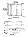
- Figure 11 shows in more detail an embodiment of one of the imaging chips, indicated at reference character 150.
- the image chip comprises a 64 x 64 rectilinear array of individual detector elements, each comprising a photodiode.
- the detector elements are arranged in 64 rows and columns.
- one such row comprises individual detector elements D1,1-D1,64.
- Sixty-four rows of detector elements are present on the imaging chip, extending downwardly to the row comprising individual detector elements D64,1-D64,64.
- a shift register including cells 01-064 is coupled in parallel to the column of detector elements Dl,l-D64,1.
- the image chip, and the detector as a whole move to the right as indicated by the arrow in Figure 11.
- the shifting and integration circuitry cause accumulating charge motion in a direction to the left as shown in Figure 11, synchronously with the detector motion in the opposite direction.
- the charge packets are transferred in parallel to the shift register, i.e., into each of the cells 01-064.
- the data thus accumulated can be clocked out, digitized, and processed to yield image representations in a manner known in the art.
- the 64 x 64 array of individual detector elements of the image chip 150 of Figure 11 collectively describe a square of 8 millimeters length on a side.
- the detector 14 comprises a vertical column of such imaging chips, each being 8 millimeters wide, and the spread beam incident on the detector is vertically oriented and 8 millimeters in thickness, just sufficient to illuminate the entirety of the vertical column of imaging chips.
- Figure 12 illustrates another embodiment of an image chip indicated by the reference character 170.
- the image chip 170 comprises a 64 x 256 array of rectangular individual detector elements.
- the array comprises 64 horizontal rows of 256 elements each.
- Each individual element has a horizontal width which is approximately 1/4 its vertical height.
- the 64 x 256 detector array describes a square approximately 8 millimeters on a side.
- the detector during scanning, is moved to the right as shown in Figure 12, and the charge packets are shifted and integrated to the left, at a rate synchronous with that of detector motion.
- the embodiment of Figure 12 is considered particularly suitable for the use of time delay and integrate circuitry consisting of CCD elements.
- the 64 x 64 array of Figure 11 is considered more suitable for the use of bucket brigade circuitry which can handle wider charge "bins", and hence has a greater capability than CCD for shifting charge packets efficiently. Efficiencies of at least about 0.99995 are desirable.
- the charges are shifted to the left, as shown in Figure 11 in synchronism with detector scanning motion.
- Data respectively corresponding to projections of the same image line is integrated and transferred along each element until the charge reaches the extreme left-hand detector element in the leftmost column of detector elements, i.e. Dl,l-D64,l.
- the charge packets are transferred and clocked successively through a series of parallel shift registers Sl-S8.
- the clocking through the registers Sl through S8 is at the same rate as the clocking along the various detector elements. No integration, however, takes place in the shift registers.
- circuitry of known type is provided which, in conjunction with the shift registers S1-S8, periodically sums output data in the shift registers S1-S8. After each succession of four shifts, the data in S1-S4, corresponding to each separate element row, is separately summed in appropriate output register circuitry, and then clocked out to digitization circuitry and image processing circuitry such as described in connection with Figure 11.
- Figure 13 is a block diagram showing circuitry of the matrix array of an image chip in greater detail.
- the image chip shown comprises a 64 x 64 element bucket brigade matrix array for detecting x-rays after they have been converted to light, similar to that of Figure 11.
- the matrix array is operated in a time delay integration mode.
- the center-to-center spacing of the individual detector elements in both the column and row directions is 5 mils.
- the array is integrated using a double poly-silicon gate NMOS process. The design details and dynamic range consideration of the image chip array are discussed in detail below.
- the image chip includes 64 horizontal bucket brigade (BBD) shift registers 201-264. Also included is a 128 element BBD shift register 265.
- BBD horizontal bucket brigade
- Each of the registers 201-265 is provided with a fat-zero input port (designated generally by reference characters 270, 272) for enhancing charge transfer efficiency in the registers.
- Registers 201-264 perform the time delay and integrate (TDI) function while register 265 transfers the signal charge package to an output sensing amplifier 274.
- the output sensing amplifier converts the charge to a signal voltage appearing at a lead 276 which is a function of the charge input to the amplifier.
- the signal at the lead 276 provides a video output.
- the center-to-center spacing of the registers 201-264 is 5 mils.
- Each of the registers 201-264 comprises 64 BBD elements (32 stages) and is driven by a two-phase complementary clock having inputs designated by the reference characters 280, 282.
- Each BBD element is constructed with a diffused photodiode and a poly-silicon-to-poly-silicon storage capacitor.
- the sensing area of each photodiode is approximately 50% of the total area of the individual detector element receiving surface.
- the capacitance of each individual detector element is about 1.2 picofarads (pF).
- the two-phase clocks at the leads 280, 282 shift the charge packages along each of the shift registers 201-264 toward the register 265.
- the clocking rates of the signals at the leads 280, 282 is approximately 0.5 kilohertz (kHz).
- the total integratioh time of each pixel is approximately 64 milliseconds (msec).
- This relatively slow integration time allows a tolerance for x-ray tube rotor and voltage ripple, and substantially reduces their artifacts.
- the register 265 is driven by a two-phase clock having inputs 292, 294. This clock signal runs at a frequency 64 times faster than that of the clock signals at the leads 280, 282.
- the output sensing amplifier of the register 265 is a gated charge integrator which converts the signal charges into output voltages.
- the clock waveforms 280, 282 and 292, 294 are complementary clocks, cross over at 50%.
- the rising edge of waveform 292 leads that of waveform 295 by about 30 nanoseconds (ns.) and waveform 295 leads waveform 280 by about 20 ns.
- the falling edge of waveform 295 leads that of waveform 292 by at least 30 ns.
- the charge handling capacity of the BBD elements depends upon the size of the storage capacitor and of the clock voltage. Assuming a maximum voltage swing of 5 volts at each BBD storage node, the saturation charge of each BBD element will be about 6 picocou- lombs (pC), i.e., 1.2 pF x 5 v. This saturation charge is equivalent to a signal charge of 3.75 x 10 7 electrons.
- noise components there are two noise components in the signal output from the sensing amplifier.
- One is the fixed-pattern noise caused by nonuniformity of the input fat-zero among the registers 201-264. This noise component can be eliminated by external signal processing. Therefore it is not the limiting factor in the performance of the device.
- thermodynamic noise The other noise component is the thermodynamic noise.
- This noise consists of input kT noise, BBD transfer noise, dark current shot noise, photo signal shot noise and output amplifier noise.
- the dominant thermodynamic noise is BBD transfer noise.
- the noise electron charge due to this component, is approximately 6000 electrons. This noise figure results in a dynamic range of about 6250 (3.75 x 10 7 /10 3 ) for the device.
Landscapes
- Health & Medical Sciences (AREA)
- Life Sciences & Earth Sciences (AREA)
- Medical Informatics (AREA)
- Engineering & Computer Science (AREA)
- Radiology & Medical Imaging (AREA)
- Molecular Biology (AREA)
- Biophysics (AREA)
- Nuclear Medicine, Radiotherapy & Molecular Imaging (AREA)
- Optics & Photonics (AREA)
- Pathology (AREA)
- Physics & Mathematics (AREA)
- Biomedical Technology (AREA)
- Heart & Thoracic Surgery (AREA)
- High Energy & Nuclear Physics (AREA)
- Surgery (AREA)
- Animal Behavior & Ethology (AREA)
- General Health & Medical Sciences (AREA)
- Public Health (AREA)
- Veterinary Medicine (AREA)
- Apparatus For Radiation Diagnosis (AREA)
- Analysing Materials By The Use Of Radiation (AREA)
Applications Claiming Priority (2)
| Application Number | Priority Date | Filing Date | Title |
|---|---|---|---|
| US54238483A | 1983-10-17 | 1983-10-17 | |
| US542384 | 1983-10-17 |
Publications (1)
| Publication Number | Publication Date |
|---|---|
| EP0138625A2 true EP0138625A2 (de) | 1985-04-24 |
Family
ID=24163598
Family Applications (1)
| Application Number | Title | Priority Date | Filing Date |
|---|---|---|---|
| EP19840307147 Withdrawn EP0138625A2 (de) | 1983-10-17 | 1984-10-17 | Röntgengerät |
Country Status (2)
| Country | Link |
|---|---|
| EP (1) | EP0138625A2 (de) |
| JP (1) | JPS60100947A (de) |
Cited By (6)
| Publication number | Priority date | Publication date | Assignee | Title |
|---|---|---|---|---|
| EP0279294A1 (de) * | 1987-02-16 | 1988-08-24 | Siemens Aktiengesellschaft | Zahnärztliche Röntgendiagnostikeinrichtung zur Erstellung von Panorama-Schichtaufnahmen vom Kiefer eines Patienten |
| US4823369A (en) * | 1987-02-16 | 1989-04-18 | Siemens Aktiengesellschaft | Dental x-ray diagnostics installation for producing panorama slice exposures of the jaw of a patient |
| EP0357944A1 (de) * | 1988-08-12 | 1990-03-14 | Siemens Aktiengesellschaft | Zahnärztliche Röntgendiagnostikeinrichtung zur Erstellung von Panorama-Schichtaufnahmen vom Kiefer eines Patienten |
| FR2663530A1 (fr) * | 1990-09-24 | 1991-12-27 | Cicolella Guilhem | Perfectionnement au dispositif pour equiper la tete d'un tomodensitometre de cellules de reference et de mesure. |
| FR2720259A1 (fr) * | 1994-05-31 | 1995-12-01 | Trophy Radiologie | Appareil de radiodiagnostic du type à capteur à transfert de charge. |
| WO1997033160A1 (de) * | 1996-03-08 | 1997-09-12 | Fraunhofer-Gesellschaft zur Förderung der angewandten Forschung e.V. | Verfahren und vorrichtung zur automatischen radioskopischen qualitätskontrolle von nahrungsmitteln |
-
1984
- 1984-10-17 EP EP19840307147 patent/EP0138625A2/de not_active Withdrawn
- 1984-10-17 JP JP59218172A patent/JPS60100947A/ja active Pending
Cited By (9)
| Publication number | Priority date | Publication date | Assignee | Title |
|---|---|---|---|---|
| EP0279294A1 (de) * | 1987-02-16 | 1988-08-24 | Siemens Aktiengesellschaft | Zahnärztliche Röntgendiagnostikeinrichtung zur Erstellung von Panorama-Schichtaufnahmen vom Kiefer eines Patienten |
| US4823369A (en) * | 1987-02-16 | 1989-04-18 | Siemens Aktiengesellschaft | Dental x-ray diagnostics installation for producing panorama slice exposures of the jaw of a patient |
| US4878234A (en) * | 1987-02-16 | 1989-10-31 | Siemens Aktiengesellschaft | Dental x-ray diagnostics installation for producing panorama slice exposures of the jaw of a patient |
| EP0357944A1 (de) * | 1988-08-12 | 1990-03-14 | Siemens Aktiengesellschaft | Zahnärztliche Röntgendiagnostikeinrichtung zur Erstellung von Panorama-Schichtaufnahmen vom Kiefer eines Patienten |
| US4995062A (en) * | 1988-08-12 | 1991-02-19 | Siemens Aktiengesellschaft | X-ray diagnostics installation for producing panorama tomograms of the jaw of a patient |
| FR2663530A1 (fr) * | 1990-09-24 | 1991-12-27 | Cicolella Guilhem | Perfectionnement au dispositif pour equiper la tete d'un tomodensitometre de cellules de reference et de mesure. |
| FR2720259A1 (fr) * | 1994-05-31 | 1995-12-01 | Trophy Radiologie | Appareil de radiodiagnostic du type à capteur à transfert de charge. |
| EP0685201A1 (de) * | 1994-05-31 | 1995-12-06 | Trophy Radiologie | Röntgendiagnostikeinrichtung mit Szintillator und CCD-Sensor |
| WO1997033160A1 (de) * | 1996-03-08 | 1997-09-12 | Fraunhofer-Gesellschaft zur Förderung der angewandten Forschung e.V. | Verfahren und vorrichtung zur automatischen radioskopischen qualitätskontrolle von nahrungsmitteln |
Also Published As
| Publication number | Publication date |
|---|---|
| JPS60100947A (ja) | 1985-06-04 |
Similar Documents
| Publication | Publication Date | Title |
|---|---|---|
| EP0166567A2 (de) | Vorrichtung und Verfahren zur Bilderzeugung | |
| US4383327A (en) | Radiographic systems employing multi-linear arrays of electronic radiation detectors | |
| US4179100A (en) | Radiography apparatus | |
| EP0176314B1 (de) | Röntgen-Anordnung | |
| US4298800A (en) | Tomographic apparatus and method for obtaining three-dimensional information by radiation scanning | |
| US4878234A (en) | Dental x-ray diagnostics installation for producing panorama slice exposures of the jaw of a patient | |
| US4426721A (en) | X-ray intensifier detector system for x-ray electronic radiography | |
| USRE37536E1 (en) | Split energy level radiation detection | |
| US6078643A (en) | Photoconductor-photocathode imager | |
| US5712889A (en) | Scanned volume CT scanner | |
| US4389729A (en) | High resolution digital radiography system | |
| EP0031732A2 (de) | Licht- und Körperschen-Bildverstärker | |
| EP0444869A2 (de) | Verfahren und Vorrichtung zur Bilderfassung | |
| EP0693225A1 (de) | Roentgenstrahlungsdetektor fuer einen digitalen, niederdosen-raster-roentgenbildwandler | |
| EP0051350B1 (de) | Abtastblende zur Darstellung einer Absorptionsverteilung mittels eines Sichtgerätes | |
| WO1991011813A1 (en) | Detector arrangement for a ct device | |
| US4164657A (en) | Apparatus for tomography | |
| JPH0510638B2 (de) | ||
| USRE32164E (en) | Radiographic systems employing multi-linear arrays of electronic radiation detectors | |
| EP0138625A2 (de) | Röntgengerät | |
| USRE32779E (en) | Radiographic systems employing multi-linear arrays of electronic radiation detectors | |
| EP0140695A2 (de) | Digitaler Röntgenaufnahmeapparat | |
| GB2186149A (en) | Image differencing using masked CCD | |
| EP0263210B1 (de) | Röntgenbildaufnahmegerät mit hohem Kontrast | |
| EP1481262B1 (de) | Vorrichtung und verfahren zur erkennung von strahlung |
Legal Events
| Date | Code | Title | Description |
|---|---|---|---|
| PUAI | Public reference made under article 153(3) epc to a published international application that has entered the european phase |
Free format text: ORIGINAL CODE: 0009012 |
|
| AK | Designated contracting states |
Designated state(s): DE FR GB NL |
|
| STAA | Information on the status of an ep patent application or granted ep patent |
Free format text: STATUS: THE APPLICATION IS DEEMED TO BE WITHDRAWN |
|
| 18D | Application deemed to be withdrawn |
Effective date: 19861103 |
|
| RIN1 | Information on inventor provided before grant (corrected) |
Inventor name: DEMEESTER, GORDON D. Inventor name: MATTSON, RODNEY A. |