EP0138547B1 - Spectral emphasis and de-emphasis circuits - Google Patents
Spectral emphasis and de-emphasis circuits Download PDFInfo
- Publication number
- EP0138547B1 EP0138547B1 EP84306848A EP84306848A EP0138547B1 EP 0138547 B1 EP0138547 B1 EP 0138547B1 EP 84306848 A EP84306848 A EP 84306848A EP 84306848 A EP84306848 A EP 84306848A EP 0138547 B1 EP0138547 B1 EP 0138547B1
- Authority
- EP
- European Patent Office
- Prior art keywords
- emphasis
- signal
- spectral
- predominant
- frequency
- Prior art date
- Legal status (The legal status is an assumption and is not a legal conclusion. Google has not performed a legal analysis and makes no representation as to the accuracy of the status listed.)
- Expired - Lifetime
Links
Images

Classifications
-
- H—ELECTRICITY
- H03—ELECTRONIC CIRCUITRY
- H03G—CONTROL OF AMPLIFICATION
- H03G7/00—Volume compression or expansion in amplifiers
- H03G7/06—Volume compression or expansion in amplifiers having semiconductor devices
-
- H—ELECTRICITY
- H04—ELECTRIC COMMUNICATION TECHNIQUE
- H04B—TRANSMISSION
- H04B1/00—Details of transmission systems, not covered by a single one of groups H04B3/00 - H04B13/00; Details of transmission systems not characterised by the medium used for transmission
- H04B1/62—Details of transmission systems, not covered by a single one of groups H04B3/00 - H04B13/00; Details of transmission systems not characterised by the medium used for transmission for providing a predistortion of the signal in the transmitter and corresponding correction in the receiver, e.g. for improving the signal/noise ratio
-
- H—ELECTRICITY
- H03—ELECTRONIC CIRCUITRY
- H03G—CONTROL OF AMPLIFICATION
- H03G5/00—Tone control or bandwidth control in amplifiers
- H03G5/16—Automatic control
-
- H—ELECTRICITY
- H03—ELECTRONIC CIRCUITRY
- H03G—CONTROL OF AMPLIFICATION
- H03G9/00—Combinations of two or more types of control, e.g. gain control and tone control
- H03G9/02—Combinations of two or more types of control, e.g. gain control and tone control in untuned amplifiers
- H03G9/025—Combinations of two or more types of control, e.g. gain control and tone control in untuned amplifiers frequency-dependent volume compression or expansion, e.g. multiple-band systems
-
- H—ELECTRICITY
- H03—ELECTRONIC CIRCUITRY
- H03M—CODING; DECODING; CODE CONVERSION IN GENERAL
- H03M3/00—Conversion of analogue values to or from differential modulation
- H03M3/02—Delta modulation, i.e. one-bit differential modulation
- H03M3/022—Delta modulation, i.e. one-bit differential modulation with adaptable step size, e.g. adaptive delta modulation [ADM]
-
- H—ELECTRICITY
- H04—ELECTRIC COMMUNICATION TECHNIQUE
- H04B—TRANSMISSION
- H04B14/00—Transmission systems not characterised by the medium used for transmission
- H04B14/02—Transmission systems not characterised by the medium used for transmission characterised by the use of pulse modulation
- H04B14/06—Transmission systems not characterised by the medium used for transmission characterised by the use of pulse modulation using differential modulation, e.g. delta modulation
Definitions
- This invention relates to a spectral emphasis circuit comprising a spectral analysis circuit providing a control signal indicative of the predominant frequency region of an input information signal, and an adaptive circuit controlled by the control signal to impose a variable emphasis or de-emphasis characteristic on the input information signal.
- the invention further relates to a spectral de-emphasis circuit for use with the emphasis circuit.
- a spectral emphasis circuit of the indicated above is known fro US-A-4,101,849, where the circuit is used in conjunction with a high-frequency compressor or expander to reduce noise modulation effects.
- a control signal is derived in dependence on the relative levels of signals passed by feed high and low frequency filters.
- the so-called pre-emphasis circuit precedes a wide-band logarithmic analog compressor and actually applies a boost or cut (de-emphasis) to the low frequency region in conjunction with the high frequency compression, depending on whether the dominant signal is in the high or low frequency region.
- a complementary circuit follows the expander.
- the present invention is concerned in particular with problems which arise when an audio or other signal is subjected to analogue to digital (A-D) conversion before transmission and then subjected to digital to analogue (D-A) conversion after transmission.
- A-D analogue to digital
- D-A digital to analogue
- the step-size used increases with the level of the input signal. Since quantizing noise increases with the step-size the quantizing noise of such adaptive systems increases with the input signal level, an example of the effect known as noise modulation.
- noise modulation an example of the effect known as noise modulation.
- the effects of noise modulation is disturbing in many applications, such as in high quality audio.
- spurious spectral information is much less audible if it is close in frequency to the desired audio signal. If the spurious energy lies far from the desired audio signal frequency it is much more likely to be audible.
- the noise level is a function of the input signal level it is particularly important to reduce noise whose frequencies are far from the desired audio signal.
- sliding band reduces audible high frequency noise by way of a filter with a variable corner frequency. As the level of high frequency signals increases, the filter corner frequency slides upwardly to narrow the band boosted and cut. Examples of such circuits are to be found in US-PS Re 28,426, US-PS 4,072,914 and US-PS 3,934,190.
- the sliding of the filter corner frequency depends on both the amplitude and frequency of the input signal. If such a "sliding band" type circuit is used to reduce audible noise that is a function of input signal level, low frequency noise may also be increased when the predominant spectral components of the input signal are at very high frequencies. While such a problem is not as serious as in the case of the high frequency fixed emphasis and de-emphasis, the "sliding band" type circuit is not entirely satisfactory for reducing noise which increases with signal level.
- US-A-3,678 416 discloses a dynamic noise filter with variable high pass and low pass filters which are used to leave only a middle frequency region unfiltered, the cut-off points of the filters being controlled by control signals with fast attack and slow decay.
- This reference also discloses a click suppressor which switches paths, with a suitable delay, when a click is detected in order to pass the signal via a sample and hold circuit and cut out the click.
- the present invention is concerned with the type of circuit defined in the first paragraph above where there is a control signal which is dependent essentially upon the spectral content of the input signal, not upon the amplitude of spectral components.
- the problem underlying the invention in a first aspect is that of allowing the control signal to be handled in a non-critical way. This leads to several possibilities for saving in circuit complexity and expense, as will be explained below.
- the spectral emphasis circuit according to a first aspect of the invention is characterized in that the control signal is bandwidth limited so as to change slowly relative to the input signal, and by a first delay circuit delaying the input signal to the adaptive circuit to compensate for the slow response of the control signal.
- the invention makes use of the observation that in order to reduce noise whose level is a function of the input signal level, the different spectral components of the input signal may be altered depending on the spectral composition of the input signal by subjecting the input signal to emphasis and subsequent de-emphasis in a complementary manner to recover an output signal which is substantially similar to the input signal.
- the spectral emphasis and de-emphasis circuits of this invention are particularly advantageous for reducing audible quantizing noise in many adaptive A-D and D-A coding systems.
- the spectral emphasis circuit may further comprise means for transmitting the information signal subjected to emphasis and means for also transmitting the control signal, the information signal being transmitted with a delay relative to the control signal corresponding to the delay provided by the first delay circuit.
- the de-emphasis circuit can then receive the transmitted information and control signals and comprises an adaptive circuit imposing on the received information signal a variable de-emphasis characteristic complementary to the variable emphasis characteristic imposed in the emnphasis circuit, the adaptive circuit being controlled by the received control signal.
- the invention further provides a spectral de-emphasis circuit according to claim 9 and a complementary emphasis/de-emphasis method as defined in claim 17.
- the spectral emphasis circuit of the invention is characterized in that when the predominant signal components are concentrated in a first frequency range, the variable characteristic consists of a sliding high-frequency boost with its corner frequency sliding upwards in response to the control signal to stay above the frequencies of the predominant signal components leaving the predominant signal components substantially unchanged, whereas when the predominant bit signal components are concentrated in a second frequency range with frequencies above those of the first frequency range, the variable characteristic of the emphasis consists of sliding high-frequency boost with its corner frequency above those of the predominant bit signal components but a cut at the frequencies of the predominant signal components themselves.
- the restoring or spectral de-emphasis circuit is characterized by an adaptive circuit controlled by the control signal to impose a variable de-emphasis characteristic on the input information signal, so that when the predominant signal components are concentrated in a first frequency range, the variable de-emphasis characteristic consists of a sliding high-frequency cut with its corner frequency sliding upwards in response to the control signal to stay above the frequencies of the predominant signal components leaving the predominant signal components substantially unchanged, whereas when the predominant signal components are concentrated in a second frequency range with frequencies above those of the first frequency range, the variable de-emphasis characteristic consists of sliding high-frequency cut with its corner frequency above those of the predominant signal components but a boost at the frequencies of the predominant signal components themselves.
- Such circuits are particularly advantageous for reducing noise which increases with signal level as well as signal frequency.
- spectral composition altering and restoration circuits of this invention are particularly suitable for reducing noise which is a function of signal level.
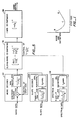
- FIGs. 2A and 2B are block diagrams for an adaptive A-D encoder and D-A decoder system which includes a pre-processing circuit and a post-processing circuit for altering and restoring the spectral composition of signals to illustrate this invention.
- the derivation, transmission and processing of step-size information in the encoder-decoder system is the subject of the companion application No.
- the noise and distortion emerging from an ADM encoder-decoder system depend on the audio input signal and the step-size, both of which are varying.
- codec ADM encoder-decoder system
- the output noise and distortion will vary as shown qualitatively in Fig. 1.
- the step-size is too large, which produces excessive quantizing noise.
- region B the step-size is too small and the system is in overload which produces high noise and distortion.
- step-size There is an optimum value of step-size for the particular input condition labelled C. For each short time segment of real audio there is a curve like that of Fig. 1, and an optimum step-size.
- the step-size In a conventional output controlled ADM system the step-size rarely achieves the optimum value, but remains in region A most of the time, moving into region B on signal transients.
- the object of this invention is to design an ADM system that operates as much as possible in region C, and that operates so that the delta modulator is fully loaded. This is possible because the step-size determination is done in the encoder and is input controlled as explained below.
- Fig. 2A is a block diagram for an encoder illustrating an embodiment of this invention.
- an analog audio input signal 12 is passed through a low-pass filter 14 to determine the overall audio bandwidth of the analog input signal. Typically such bandwidth may be 15 kHz.
- the analog input signal is then passed through a pre-processing circuit 16. The function of the pre-processing circuit 16 will be discussed below.
- the analog audio input signal is supplied to a step-size derivation circuit 18 and to a delay circuit 20.
- the step-size derivation circuit 18 comprises a slope detector for detecting the time derivative or slope of the incoming audio input signal.
- the slope detector then generates a control signal indicative of the step-size to be used in the adaptive delta modulator 22.
- the control signal is limited by a bandwidth limitation circuit 24 and then applied to the adaptive delta modulator 22.
- A-D converter 26 converts the step-size control signal into a bit-stream of digital signals to convey step-size information.
- the audio input signal After being time delayed by delay circuit 20 the audio input signal is converted into a bit-stream of digital audio signals by adaptive delta modulator 22 in accordance with the step-size indicated by the bandwidth limited step-size control signal 45.
- the audio bit-stream and the step-size information bit-stream are then transmitted through a medium to a decoder which is shown in Fig. 2B.
- encoder 10 is part of a broadcasting station transmitting the audio and step-size information bit-streams to decoders in consumer systems.
- the function of delay circuit 20 and bandwidth limitation circuit 24 will be discussed after a brief description of the decoder of Fig. 2B below.
- Fig. 2B is a block diagram of a decoder illustrating the preferred embodiment of this invention.
- decoder 40 comprises an adaptive delta demodulator 42 for receiving the digital audio bit-stream 30 transmitted through the medium and a D-A converter 44 for receiving the digital step-size information bit-stream 28.
- D-A converter 44 converts the digital bit-stream into an analog step-size control signal which is supplied to bandwidth limitation circuit 46.
- the step-size control signal is applied to adaptive delta demodulator 42.
- Adaptive delta demodulator 42 generates an analog audio output signal from the audio bit-stream in accordance with bandwidth limited step-size control signal from bandwidth limitation 46.
- bandwidth limitation circuit 46 limits the bandwidth of the step-size control signal applied to adaptive delta-demodulator 42.
- delay circuit 20 introduces a time delay so that the pre-processed analog audio input signal will reach adaptive delta modulator 22 at a time when the step-size control signal for such input signal is available from bandwidth limitation circuit 24. This is particularly advantageous when there are sudden changes in the slope of the input audio signal.
- bit-stream 28 and audio bit-stream 30 are shown as being transmitted separately, it will be understood that the two bit-streams may be transmitted together in one single channel provided that the two bit-streams can be distinguished from each other. Similarly, all three bit-streams 28, 30 and 82 may also be transmitted in the same channel instead of in separate channels if they can be distinguished from each other.
- the audio bit-stream signals which are the digital representation of a particular analog signal reach the delta demodulator when the bandwidth limited step-size control signal is available from circuit 46.
- the need for a delay circuit in the decoder to compensate for the time delay caused by the bandwidth limiting of the step-size control signal in the decoder is eliminated and the decoder circuit is simplified. This is particularly advantageous for lowering the cost of consumer decoder equipment.
- the pre-processing and post-processing circuits 16, 96 and other associated circuit components illustrate this invention. Since the step-size in the A-D and D-A conversions is variable, the noise amplitude will be modulated depending on the step-size and such noise modulation is undesirable in many applications such as in high quality audio equipment. Noise modulation is reduced by pre-processing circuit 16 and post-processing circuit 96 when combined with components A-D converter 72 and digital delay 74 of Fig. 2A.
- the pre-processing circuit 16 comprises spectral analysis circuit 52, bandwidth limitation circuit 54, adaptive pre-emphasis circuit 56, and delay circuit 58, all of Fig. 2A.
- the post-processing circuit 96 comprises D-A converter 76, adaptive de-emphasis circuit 78 and bandwidth limitation circuit 80, all of Fig. 2B.
- Spectral analysis circuit 52 analyzes the audio input signal to generate an emphasis control signal.
- the emphasis control signal generated is a function only of the spectrum of the input audio and is substantially independent of the amplitude of the input audio.
- the emphasis control signal is then limited by bandwidth limitation circuit 54 and applied to adaptive pre-emphasis circuit 56.
- Adaptive pre-emphasis circuit 56 boosts or boosts and bucks the different frequency components of the input audio signal by amounts which are functions of the emphasis control signal.
- the emphasis control signal is limited in bandwidth so that the frequency response of the adaptive pre-emphasis circuit 56 will not change suddenly from sample to sample.
- Bandwidth limitation circuit 80 reduces the effect of bit errors introduced by the transmission medium in a manner similar to bandwidth limitation circuit 46 described above.
- delay circuit 58 introduces a time delay which permits the pre-emphasis circuit 56 to complete its adaptation before the audio input signal is supplied to the pre-emphasis circuit 56.
- the pre-processed audio input signal is supplied to delay circuit 20 and adaptive delta modulator 22 as described above.
- the emphasis control signal from spectral analysis circuit 52 is converted into a digital bit-stream carrying spectral information by A-D converter 72 and is delayed by digital delay 74 by a time period substantially equal to that of delay circuit 20.
- an audio signal in the audio bit-stream has been delayed by delay circuits 58, 20, whereas the corresponding spectral information signal for such audio signal has been delayed by only the digital delay 74.
- the net effect is that the audio is delayed relative to the corresponding spectral information by the time delay caused by delay 58, so that the spectral information reaches the decoder of Fig. 2B and the post-processing circuit 96 in advance of the corresponding audio signals and at the proper time to change the amplitudes of the various frequency components of the audio signal in a manner complementary to that of the adaptive pre-emphasis circuit 56.
- the time delay introduced in the encoder by circuit 58 compensates for the time delay caused by bandwidth limiting the spectral information in bandwidth limitation circuit 80 in the decoder.
- bandwidth limitation circuit 80 would cause the audio to reach the adaptive de-emphasis 78 before the bandwidth limited de-emphasis control signal was available for controlling the de-emphasis.
- a delay circuit would then be required in the decoder to delay the audio so that the audio would reach the de-emphasis 78 at the appropriate time.
- One of the purposes of the encoder-decoder system of Figs. 2A and 2B is to transmit an analog audio signal through a medium so that the analog audio output signal recovered after the transmission is substantially the same as the input audio.
- the adaptive delta modulator 22 in the encoder of Fig. 2A and the adaptive delta demodulator 42 are substantially complementary to each other.
- the step-size control signals applied to the modulator 22 and demodulator 42 are substantially the same and are applied to the modulator and demodulator with substantially the same timing relationship with respect to the corresponding audio signals so that the modulation and demodulation applied are complementary.
- the step-size control signal for an audio signal is applied at a time t before or after the audio signal reaches the modulator 22, the step-size control signal should reach the demodulator 42 also at substantially time t before or after the audio signal reaches the demodulator.
- the pre-processing and post-processing circuits are also substantially complementary to each other; the emphasis and de-emphasis control signals are substantially the same and have substantially the same timing relationship with respect to the audio for the application of pre-emphasis and de-emphasis so that the pre-emphasis and de-emphasis applied are substantially complementary.
- the encoder-decoder system is highly tolerant of timing errors. Since the step-size, pre-emphasis and de-emphasis control signals can only change slowly in the encoder and decoder, the adaptive modulation and demodulation together with the pre-emphasis and de-emphasis applied by the encoder and decoder can only change slowly. Thus mismatch in timing relationship of the type discussed above and of the order of a few percent of the bandwidth limitation rise times will not cause the modulation and demodulation to deviate significantly from being complementary. Similarly mismatch in timing relationship of such order of magnitude will not cause the pre-emphasis and de-emphasis applied to deviate significantly from being complementary.
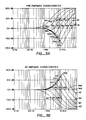
- Figs. 3A, 3B The characteristics of adaptive pre-emphasis and de-emphasis circuits 56, 78 are illustrated in Figs. 3A, 3B. It will be understood that the specific frequencies and gains in Figs. 3A, 3B and in the discussion below are for illustrative purposes only and that the characteristics of circuits 56, 78 are not limited thereby.
- the pre-emphasis and de-emphasis characteristics are similar to the well known type of "sliding band" circuits, which reduce high frequency noise by way of a filter with a variable corner frequency. As the signal level increases, the filter corner frequencies of such "sliding band” circuits slide continuously and upwardly to narrow the band boosted and cut. Examples of such circuits are found in US-PS Re 28,426; US-PS 4,072,914 and US-PS 3,934,190.
- the pre-emphasis characteristic of circuit 56 also has a variable frequency indicated at 86a, 88a, 90a, 92a, 94a and 96a of the pre-emphasis characteristic curves 86, 88, 90, 92, 94 and 96 respectively of Fig. 3A.
- the de-emphasis curves 84'-96' of Fig. 3B are complementary to curves 84-96 respectively and also have variable frequencies 86a'-96a'.
- Such variable frequencies also continuously shift as a function of the input audio.
- the continuous shifting is determined, not by the level of high frequency signals but by the spectral content of the input audio in a manner described below.
- adaptive pre-emphasis circuit 56 adopts the response labelled 84, boosting only signals with frequencies above 500 Hz; the predominant signals with frequencies below 500 Hz remain substantially unchanged. In other words, there is a high frequency boost with a minimum corner frequency of 500 Hz. This minimum corner frequency could alternatively be 1000 Hz.
- adaptive de-emphasis circuit 78 When the audio signal from the adaptive delta-demodulator 42 reaches adaptive de-emphasis circuit 78 the high frequency components of the quantizing noise will be reduced by adaptive de-emphasis circuit 78 which will have a characteristic 84' complementary to curve 84 as shown in Figs 3A and 3B. High frequency noise above 500 Hz is thereby reduced sufficiently that audible noise modulation becomes much diminished. Low and medium frequency noise below 500 Hz is masked by the signal.
- the emphasis control signal from the spectral analysis circuit 52 causes the frequency response of adaptive pre-emphasis circuit 56 to slide from 84 to 86 or 88, i.e. the corner frequency slides upwardly.
- Such dynamic action of the adaptive pre-emphasis circuit prevents undesirable increases in the step-size of the adaptive delta-modulator but still allows the subsequent complementary de-emphasis to reduce noise at frequencies above those of the input signal. Low frequency noise is not yet an audible problem.
- the frequency responses of the shape 84, 86, 88 are satisfactory for noise reduction when the predominant spectral components of the input audio signal are below 2 or 3 kHz. Noise at frequencies above these predominant spectral components is reduced as described above; lower frequency noise is masked by the signal.
- the predominant spectral components of the input audio signal are at high frequencies (e.g.above 3 kHz) such sliding boost responses may no longer be satisfactory for noise reduction, since low and medium frequency noise is no longer masked by the signal. Under these signal conditions the effect of high frequency boost would be to increase the step-size employed in the adaptive delta modulator 22 and demodulator 42, resulting in an increase in wide-band quantizing noise.
- the subsequent complementary high frequency cut would not reduce the low frequency part of this increased noise.
- low frequency noise would be modulated by changes in the high frequency components of the input audio signal.
- curves 90, 92, 94 and 96 at frequencies above the variable frequency retain the shape of a high frequency shelf.
- curves 84, 86, 88 tend towards the same fixed gain (eg. 20 dB) at high frequencies.
- curves 90-96 also tend towards the same fixed gain at still higher frequencies.
- the complementary de-emphasis curves 84'-96' corresponding to respective pre-emphasis curves 84-96 are shown in Fig. 3B, and have variable frequencies 86a'-96a' which are substantially the same as those of the pre-emphasis curves.
- De-emphasis curves 90'-96' have peaks 90b'-96b' corresponding to dips 90b-96b of the pre-emphasis curves of Fig. 3A.
- the predominant signal components of the input audio are concentrated in a certain region of the frequency spectrum.
- Such an input signal is in fact the most critical case.
- the signal spectral components are more distributed, their masking properties cover more of the noise, and the shapes of the pre-emphasis curves are less critical. If the signal spectral components are distributed in two regions of the frequency spectrum, the pre-emphasis curve will resemble the curve for the case where the spectral components are concentrated in a region between such two regions.
- Bandwidth limitation circuits 24,46, 54 and 80 limit the step-size and spectral control signals to within bandwidths of a few tens or low hundreds of Hz; hence the control signals can have rise times of a few milliseconds.
- the delay introduced by delay circuits 20, 58 is therefore chosen to be substantially equal to the rise times of the control signals as determined by the bandwidth limiting. Suitable values are in the range 5 to 20 milliseconds.
- the control A-D and D-A converters 26, 44, 72 and 76 may be simple delta or delta-sigma modulators and demodulators operating at a few kilobits per second. In television sound applications a convenient value is half the horizontal frequency, about 7.8 kHz.
- the signal entering bandwidth limitation 54 in the encoder 10 may be derived from the information bit-stream 82 instead of the output of spectral analysis 52.
- Such configuration is illustrated in Fig 4, with adaptive pre-emphasis 56, limitation circuit 54 and A-D converter 72 rearranged as shown.
- a local D-A converter 100 converts the digital step-size information from bit-stream 82 into an analog emphasis control signal.
- the circuit arrangement of Fig 4 is particularly advantageous where the A-D converter 72 uses delta-sigma modulation so that the local D-A converter 100 is already contained within the A-D converter and no extra local D-A converter will be necessary.
- the step-size information supplied to adaptive delta-modulator circuit 22 may be derived from the step-size information bit-stream 28. This is again advantageous if A-D converter 26 uses delta-sigma modulation.
- D-A converter 44 may contain the bandwidth limitation.
- bandwidth limitation circuit 80 may be eliminated if D-A converter 76 is similarly bandwidth limited.
- the A-D converter 26 and D-A converter 44 are preferable to design the A-D converter 26 and D-A converter 44 so that the digital bit-stream 28 conveys the logarithm of the step-size.
- the spectral information bit-stream preferably conveys the logarithm of the spectral information.
- some other non-linear function of the step-size such as the square root or the cube-root; such functions will not give perfectly uniform gain errors over the dynamic range of the system, but the extent of the variation will be much less than that resulting from a linear function.
- an encoder-decoder system which conveys step-size information and spectral information at low bit rates of transmission and which can be implemented at low cost.
- the scheme for A-D and D-A conversion for converters 26, 44, 72 and 76 it is desirable to choose one that allows a low bit rate for the transmission of step-size information.
- bit rate is small compared to the bit rate for transmission of audio data.
- the A-D or D-A conversion performed in converters 26, 72 and 44, 76 can be one of many schemes, including PCM, delta modulation or delta-sigma modulation.
- delta-sigma modulation requires a somewhat higher bit rate (on the order of 5 to 10 kbit/sec) than PCM but it can be implemented simply and at low cost. Furthermore, the bit rate required for delta-sigma modulation is still low compared with the bit rate for the transmission of audio data (on the order of 200 to 300 kbit/sec). Therefore, delta-sigma modulation is used in the preferred embodiment discussed below. A description of delta-sigma modulation can be found in Delta Modulation Systems , Pentech Press Limited, London, 1975 by Raymond Steele.
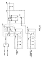
- Fig. 5 is a block diagram for a decoder system illustrating the preferred embodiment of the invention; the characteristics of most of the circuit blocks are defined for the system in Fig. 5.
- the system is particularly suitable for consumer use.
- the adaptive delta demodulator or audio decoder 42 comprises a pulse height modulator 202 and a leaky integrator 204.
- Pulse height modulator 202 multiplies the step-size control signal Vss by +1 or -1 in accordance with the audio data bit stream, and supplies the result to the leaky integrator 204.
- the leak time constant may be approximately 0.5 milliseconds which corresponds to a cut-off frequency of approximately 300 Hz.
- the integrator integrates the resulting signal to produce an analog audio signal. At frequencies below the frequency corresponding to the leak time constant, the system is strictly not delta but delta-sigma modulation.
- the adaptive delta modulator 22 also includes a leaky integrator (not shown) with a cut-off frequency which is about the same as the one in the decoder.
- the step-size derivation means 18 may be a slope detector which responds to the pre-processed input audio signal by deriving a control signal indicative of the slopes of the signal components of the audio input with frequencies above the cut-off frequency and the amplitudes of the signal components with frequencies below the cut-off frequency.
- the step-size or slope data are transmitted by delta-sigma modulation and in the form of the logarithm of the required step-size or slope.
- the slope data are therefore decoded in the slope decoder 205 by passage through a low pass filter 206 (corresponding to D-A converter 44 and bandwidth limitation 46 of Fig. 2B), which determines the bandwidth (and hence the rise-time) and ripple of the slope voltage.
- a 3-pole low pass filter is employed which causes the step-size control signal Vss to have a rise time of about 10 milliseconds corresponding to a bandwidth of about 50 Hz.
- the slope voltage is then applied to an exponentiator 208 or anti-log. circuit, which may be, for example, a bipolar transistor. If the normalized mean level of the bit stream (or the duty-cycle measured over the rise-time of the low pass filter) is written as y, then
- the transmission of slope information in logarithm form reduces the dynamic range conveyed in the slope data bit-stream from about 50 dB to about 19 dB, and spreads the effect of bit errors more uniformly across the dynamic range. Since Vss is confined by the low pass filter 206 to a bandwidth of about 50 Hz, bit errors lead to slow random amplitude modulation of the output audio. The audible disturbance produced by errors in the slope data bit-stream may be negligible. It has been observed that uncorrected bit error rates of up to 1 in 100 or so produce nearly imperceptible disturbance of music or speech.
- the low pass filter thus converts the digital slope data into analog data and limits its bandwidth.
- Low pass filter 206 therefore performs both the functions of both the D-A converter 44 and bandwidth limitation 46 of Fig. 2B.
- delay means 20 introduces such delay that the slope data are received by filter 206 before the corresponding audio data are received by the pulse height modulator 202. Such time difference compensates for the rise time of about 10 milliseconds of Vss. In such manner, the need for a delay circuit in the decodor is eliminated.
- Fig. 3B illustrates a set of de-emphasis curves which are complementary to those of the pre-emphasis curves of Fig. 3A.
- the sliding band de-emphasis 78 defined in Fig. 5 shows one practical implementation of the de-emphasis characteristic.
- the system definitions for all the circuit blocks in Fig. 5 together with one set of values of the constants giving satisfactory results are listed below:
- the spectrum decoder 212 comprising 3-pole filter 214 and exponentiator 216 is substantially the same as the slope decoder. It finds the normalized mean level x of the spectrum data input which conveys the logarithm of the variable frequency of the desired sliding band de-emphasis f1 defined above, f1 being different from the variable frequencies 86a-96a, 86a'-96a' of Figs. 3A, 3B.
- the spectrum decoder generates the exponent or anti-log. of the mean level and applies the resulting voltage or current to the sliding band de-emphasis 78.
- the emphasis control signal is even less affected by bit errors in transmission than the slope data control signal.
- Non-audio spectral components in the output are at frequencies well above the audio band and only an elementary low pass filter such as filter 118 is necessary.
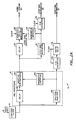
- Fig. 6 is a schematic circuit diagram showing a possible implementation of the system of Fig. 5.
- the sliding band de-emphasis circuit 78 employs a main path 78a with fixed characteristics in parallel with a further path 78b with variable characteristics.
- the variable characteristics of the further path are controlled by the resistance of a variable resistance 252, which in turn is controlled by the emphasis control signal from spectrum decoder 212.
- the further path is controlled ultimately by the spectrum of the input audio.
- the characteristics of the delta demodulator 42 and de-emphasis 78 can only change slowly. Because they have slowly changing characteristics, the delta demodulator and de-emphasis are thereby rendered linear or quasi-linear. It makes little difference whether the demodulation is performed ahead of the de-emphasis or vice versa. This linear or quasi-linear feature of the decoder system is even clearer in the case of the preferred embodiment in Fig. 5.
- Four processes are performed on the audio bit stream: pulse height modulation, leaky integration, sliding band de-emphasis and fixed de-emphasis. All four are linear or quasi-linear processes so that they can be performed in any order.
- the pulse height modulator 202 can be a relatively simple circuit since it is required only to switch the sign of voltage Vss depending on the state of the audio bit-stream.
- the modulator 202 may be made at low cost for consumer decoders.
- multiplying the audio data by the step-size control signal at a different point say after sliding band de-emphasis but before fixed de-emphasis, may have the advantage that quality of the audio output is improved. This may be desirable for applications such as in broadcast stations and other professional equipment. While the multiplication will have to be performed by a circuit more complex and therefore costlier than the type of pulse height modulator adequate for the arrangement of Fig. 5, the improvement in quality for professional applications may be well worth the additional cost. Multiplying the audio data at a different point is permissible because the four processes are effectively linear as explained above. All such possible arrangements of the four processes are within the scope of this invention.
- This invention together with the invention of the companion application referenced above reduce the transmission bit rate of the audio bit-stream to that comparable with or somewhat less than the bit rate required for a companded PCM system with comparable performance.
- the transmission bit rates for the encoder-decoder system of this invention may be in the region of 200 or 300 kbit per second.
- the transmission of spectral and step-size information may require about 10 or 23 kbit per second and does not add significantly to the total transmission bit rate required for the encoder-decoder system of this invention.
- the encoder-decoder system of Figs. 2A and 2B retains the advantages of delta modulation systems.
- the invention reduces and in many applications eliminates disturbing effects of bit errors. It and its components have high tolerance of errors.
- the receiving equipment is inexpensive.
- the system is efficient in usage of channel capacity so that more excess capacity will exist for flexibility to add additional channels or more bandwidth will be available to other signals such as video signals.
- the transmission equipment does not require special attention or require the use of non-complementary signal processing.
Description
- This invention relates to a spectral emphasis circuit comprising a spectral analysis circuit providing a control signal indicative of the predominant frequency region of an input information signal, and an adaptive circuit controlled by the control signal to impose a variable emphasis or de-emphasis characteristic on the input information signal. The invention further relates to a spectral de-emphasis circuit for use with the emphasis circuit.
- A spectral emphasis circuit of the indicated above is known fro US-A-4,101,849, where the circuit is used in conjunction with a high-frequency compressor or expander to reduce noise modulation effects. A control signal is derived in dependence on the relative levels of signals passed by feed high and low frequency filters. Depending on the control signal, the so-called pre-emphasis circuit precedes a wide-band logarithmic analog compressor and actually applies a boost or cut (de-emphasis) to the low frequency region in conjunction with the high frequency compression, depending on whether the dominant signal is in the high or low frequency region. A complementary circuit follows the expander.
- Such characteristics are unsuited to other applications of emphasis and de-emphasis. The present invention is concerned in particular with problems which arise when an audio or other signal is subjected to analogue to digital (A-D) conversion before transmission and then subjected to digital to analogue (D-A) conversion after transmission.
- In many adaptive A-D and D-A coding systems the step-size used increases with the level of the input signal. Since quantizing noise increases with the step-size the quantizing noise of such adaptive systems increases with the input signal level, an example of the effect known as noise modulation. The effects of noise modulation is disturbing in many applications, such as in high quality audio.
- It is a characteristic of human hearing that spurious spectral information is much less audible if it is close in frequency to the desired audio signal. If the spurious energy lies far from the desired audio signal frequency it is much more likely to be audible. Thus where the noise level is a function of the input signal level it is particularly important to reduce noise whose frequencies are far from the desired audio signal.
- Conventional noise reduction systems have been used to apply adaptive emphasis and de-emphasis to reduce audible noise. One conventional system employs fixed emphasis for boosting high frequency signals and complementary de-emphasis for bucking such signals. When such emphasis and de-emphasis are used to reduce audible noise that increases with signal level and when the predominant signals are of high frequencies, low frequency noise will instead be increased. Fixed high frequency emphasis and de-emphasis are therefore unsatisfactory for reducing such noise.
- A well known type of circuit, called "sliding band", reduces audible high frequency noise by way of a filter with a variable corner frequency. As the level of high frequency signals increases, the filter corner frequency slides upwardly to narrow the band boosted and cut. Examples of such circuits are to be found in US-PS Re 28,426, US-PS 4,072,914 and US-PS 3,934,190.
- The sliding of the filter corner frequency depends on both the amplitude and frequency of the input signal. If such a "sliding band" type circuit is used to reduce audible noise that is a function of input signal level, low frequency noise may also be increased when the predominant spectral components of the input signal are at very high frequencies. While such a problem is not as serious as in the case of the high frequency fixed emphasis and de-emphasis, the "sliding band" type circuit is not entirely satisfactory for reducing noise which increases with signal level.
- US-A-3,678 416 discloses a dynamic noise filter with variable high pass and low pass filters which are used to leave only a middle frequency region unfiltered, the cut-off points of the filters being controlled by control signals with fast attack and slow decay. This reference also discloses a click suppressor which switches paths, with a suitable delay, when a click is detected in order to pass the signal via a sample and hold circuit and cut out the click.
- In contrast to such prior art the present invention is concerned with the type of circuit defined in the first paragraph above where there is a control signal which is dependent essentially upon the spectral content of the input signal, not upon the amplitude of spectral components.
- The problem underlying the invention in a first aspect is that of allowing the control signal to be handled in a non-critical way. This leads to several possibilities for saving in circuit complexity and expense, as will be explained below.
- The spectral emphasis circuit according to a first aspect of the invention is characterized in that the control signal is bandwidth limited so as to change slowly relative to the input signal, and by a first delay circuit delaying the input signal to the adaptive circuit to compensate for the slow response of the control signal.
- The use of a delay circuit to compensate for the delay of a control signal smoothing circuit is known per se in other contexts. US 4,169,219 suggests this in relation to the control signal for a variable gain compressor or expander circuit. The present invention resides more in the appreciation that suitably severe bandwidth limitation can render the control signal non-critical. Some mismatch between the timings of control signals in complementary emphasis and de-emphasis circuits can be tolerated. The control signal can be transmitted so that the spectral analysis circuit is needed only in the emphasis circuit. The received control signal is subject to error (e.g. bit errors if also transmitted digitally) but will nevertheless control the de-emphasis circuit satisfactorily because it is bandwidth limited therein. Moreover, as will be shown below, the de-emphasis circuit can be further simplified by effectively placing all delay circuits in the emphasis circuit.
- The invention makes use of the observation that in order to reduce noise whose level is a function of the input signal level, the different spectral components of the input signal may be altered depending on the spectral composition of the input signal by subjecting the input signal to emphasis and subsequent de-emphasis in a complementary manner to recover an output signal which is substantially similar to the input signal. The spectral emphasis and de-emphasis circuits of this invention are particularly advantageous for reducing audible quantizing noise in many adaptive A-D and D-A coding systems.
- The spectral emphasis circuit may further comprise means for transmitting the information signal subjected to emphasis and means for also transmitting the control signal, the information signal being transmitted with a delay relative to the control signal corresponding to the delay provided by the first delay circuit.
- The de-emphasis circuit can then receive the transmitted information and control signals and comprises an adaptive circuit imposing on the received information signal a variable de-emphasis characteristic complementary to the variable emphasis characteristic imposed in the emnphasis circuit, the adaptive circuit being controlled by the received control signal.
- The invention further provides a spectral de-emphasis circuit according to claim 9 and a complementary emphasis/de-emphasis method as defined in claim 17.
- Another aspect of the invention is directed to a particular emphasis and complementary de-emphasis which when applied to a medium whose noise level is a function of the signal level in the medium, reduces noise introduced by the medium. In such aspect, the spectral emphasis circuit of the invention is characterized in that when the predominant signal components are concentrated in a first frequency range, the variable characteristic consists of a sliding high-frequency boost with its corner frequency sliding upwards in response to the control signal to stay above the frequencies of the predominant signal components leaving the predominant signal components substantially unchanged, whereas when the predominant bit signal components are concentrated in a second frequency range with frequencies above those of the first frequency range, the variable characteristic of the emphasis consists of sliding high-frequency boost with its corner frequency above those of the predominant bit signal components but a cut at the frequencies of the predominant signal components themselves.
- The restoring or spectral de-emphasis circuit is characterized by an adaptive circuit controlled by the control signal to impose a variable de-emphasis characteristic on the input information signal, so that when the predominant signal components are concentrated in a first frequency range, the variable de-emphasis characteristic consists of a sliding high-frequency cut with its corner frequency sliding upwards in response to the control signal to stay above the frequencies of the predominant signal components leaving the predominant signal components substantially unchanged, whereas when the predominant signal components are concentrated in a second frequency range with frequencies above those of the first frequency range, the variable de-emphasis characteristic consists of sliding high-frequency cut with its corner frequency above those of the predominant signal components but a boost at the frequencies of the predominant signal components themselves.
- Such circuits are particularly advantageous for reducing noise which increases with signal level as well as signal frequency.
- The invention will be described by way of example, with reference to the accompanying drawings, in which:-
- Fig. 1 is a graphical illustration of the noise distortion emerging from an adaptive delta modulation coder-decoder as a function of the step-size applied by the coder-decoder.
- Fig. 2A is a block diagram of an encoder which includes a pre-processing circuit illustrating an embodiment of this invention.
- Fig. 2B. is a block diagram of a decoder which includes a post-processing circuit illustrating the preferred embodiment of this invention.
- Figs. 3A and 3B are graphical illustrations of respectively the pre-emphasis characteristics of the pre-processing circuit of Fig. 2A and the de-emphasis characteristics of the post-processing circuit of Fig. 2B.
- Fig.4 is a block diagram illustrating the preferred embodiment for a portion of the pre-processing circuit of Fig.2A.
- Fig. 5 is a block diagram of a decoder which includes a post-processing circuit, the diagram containing the system definition of the decoder to illustrate the preferred embodiment of the invention.
- Fig. 6 is a schematic circuit diagram for the circuit of Fig. 5 to illustrate the invention.
- The spectral composition altering and restoration circuits of this invention are particularly suitable for reducing noise which is a function of signal level. Below is a description of an A-D and D-A conversion system whose noise level rises with the signal level; the description will serve as a background desirable for understanding this invention. Figs. 2A and 2B are block diagrams for an adaptive A-D encoder and D-A decoder system which includes a pre-processing circuit and a post-processing circuit for altering and restoring the spectral composition of signals to illustrate this invention. The derivation, transmission and processing of step-size information in the encoder-decoder system is the subject of the companion application No. 8430649.5, now EP-A-0 138 548 (see also divisional applications 90200454.8 and 90200455.5, now EP-A-0 376 933 and 0 384 544). The discussion that immediately follows concerning step-size determination is taken from such companion application.
- The noise and distortion emerging from an ADM encoder-decoder system (codec) depend on the audio input signal and the step-size, both of which are varying. Consider a codec handling a single sine wave. As a function of step-size, the output noise and distortion will vary as shown qualitatively in Fig. 1. In the region labelled A, the step-size is too large, which produces excessive quantizing noise. In region B the step-size is too small and the system is in overload which produces high noise and distortion. There is an optimum value of step-size for the particular input condition labelled C. For each short time segment of real audio there is a curve like that of Fig. 1, and an optimum step-size. In a conventional output controlled ADM system the step-size rarely achieves the optimum value, but remains in region A most of the time, moving into region B on signal transients. The object of this invention is to design an ADM system that operates as much as possible in region C, and that operates so that the delta modulator is fully loaded. This is possible because the step-size determination is done in the encoder and is input controlled as explained below.
- Fig. 2A is a block diagram for an encoder illustrating an embodiment of this invention. As shown in Fig. 2A, an analog
audio input signal 12 is passed through a low-pass filter 14 to determine the overall audio bandwidth of the analog input signal. Typically such bandwidth may be 15 kHz. The analog input signal is then passed through apre-processing circuit 16. The function of thepre-processing circuit 16 will be discussed below. - After being pre-processed the analog audio input signal is supplied to a step-
size derivation circuit 18 and to adelay circuit 20. In one particular application the step-size derivation circuit 18 comprises a slope detector for detecting the time derivative or slope of the incoming audio input signal. The slope detector then generates a control signal indicative of the step-size to be used in theadaptive delta modulator 22. The control signal is limited by abandwidth limitation circuit 24 and then applied to theadaptive delta modulator 22.A-D converter 26 converts the step-size control signal into a bit-stream of digital signals to convey step-size information. After being time delayed bydelay circuit 20 the audio input signal is converted into a bit-stream of digital audio signals byadaptive delta modulator 22 in accordance with the step-size indicated by the bandwidth limited step-size control signal 45. The audio bit-stream and the step-size information bit-stream are then transmitted through a medium to a decoder which is shown in Fig. 2B. In oneparticular application encoder 10 is part of a broadcasting station transmitting the audio and step-size information bit-streams to decoders in consumer systems. The function ofdelay circuit 20 andbandwidth limitation circuit 24 will be discussed after a brief description of the decoder of Fig. 2B below. - Fig. 2B is a block diagram of a decoder illustrating the preferred embodiment of this invention. As shown in Fig. 2B decoder 40 comprises an
adaptive delta demodulator 42 for receiving the digital audio bit-stream 30 transmitted through the medium and aD-A converter 44 for receiving the digital step-size information bit-stream 28.D-A converter 44 converts the digital bit-stream into an analog step-size control signal which is supplied tobandwidth limitation circuit 46. After being limited in bandwidth, the step-size control signal is applied toadaptive delta demodulator 42.Adaptive delta demodulator 42 generates an analog audio output signal from the audio bit-stream in accordance with bandwidth limited step-size control signal frombandwidth limitation 46.Bandwidth limitation circuit 24 of Fig. 2A limits the bandwidth of the step-size control signal applied to adaptive delta-modulator 22 so that the step-size cannot change abruptly from one sample to the next. Similarly,bandwidth limitation circuit 46 limits the bandwidth of the step-size control signal applied to adaptive delta-demodulator 42. Thus if the transmission medium introduces a bit error in the step-size information bit-stream, such an error, after being converted into analog form byD-A converter 44, cannot introduce a major error in the step-size atadaptive delta demodulator 42. The effect of transmission errors is thereby reduced. Therefore, cheap non-precision components may be used to construct theconverters - The generation of a limited bandwidth step-size control signal will require a finite time. To compensate for such time,
delay circuit 20 introduces a time delay so that the pre-processed analog audio input signal will reachadaptive delta modulator 22 at a time when the step-size control signal for such input signal is available frombandwidth limitation circuit 24. This is particularly advantageous when there are sudden changes in the slope of the input audio signal. - While in Figs. 2A and 2B the step-size information bit-
stream 28 and audio bit-stream 30 are shown as being transmitted separately, it will be understood that the two bit-streams may be transmitted together in one single channel provided that the two bit-streams can be distinguished from each other. Similarly, all three bit-streams - By introducing a time delay through
delay circuit 20 that also compensates for the time delay caused by thebandwidth limitation circuit 46 in the decoder, the audio bit-stream signals which are the digital representation of a particular analog signal reach the delta demodulator when the bandwidth limited step-size control signal is available fromcircuit 46. In such manner, the need for a delay circuit in the decoder to compensate for the time delay caused by the bandwidth limiting of the step-size control signal in the decoder is eliminated and the decoder circuit is simplified. This is particularly advantageous for lowering the cost of consumer decoder equipment. - The invention of this application will now be discussed. The pre-processing and
post-processing circuits circuit 16 andpost-processing circuit 96 when combined withcomponents A-D converter 72 anddigital delay 74 of Fig. 2A. Thepre-processing circuit 16 comprisesspectral analysis circuit 52,bandwidth limitation circuit 54,adaptive pre-emphasis circuit 56, anddelay circuit 58, all of Fig. 2A. Thepost-processing circuit 96 comprisesD-A converter 76, adaptivede-emphasis circuit 78 andbandwidth limitation circuit 80, all of Fig. 2B. -
Spectral analysis circuit 52 analyzes the audio input signal to generate an emphasis control signal. The emphasis control signal generated is a function only of the spectrum of the input audio and is substantially independent of the amplitude of the input audio. The emphasis control signal is then limited bybandwidth limitation circuit 54 and applied toadaptive pre-emphasis circuit 56.Adaptive pre-emphasis circuit 56 boosts or boosts and bucks the different frequency components of the input audio signal by amounts which are functions of the emphasis control signal. The emphasis control signal is limited in bandwidth so that the frequency response of theadaptive pre-emphasis circuit 56 will not change suddenly from sample to sample.Bandwidth limitation circuit 80 reduces the effect of bit errors introduced by the transmission medium in a manner similar tobandwidth limitation circuit 46 described above. - In reference to Figs. 2A, 2B,
delay circuit 58 introduces a time delay which permits thepre-emphasis circuit 56 to complete its adaptation before the audio input signal is supplied to thepre-emphasis circuit 56. The pre-processed audio input signal is supplied to delaycircuit 20 andadaptive delta modulator 22 as described above. The emphasis control signal fromspectral analysis circuit 52 is converted into a digital bit-stream carrying spectral information byA-D converter 72 and is delayed bydigital delay 74 by a time period substantially equal to that ofdelay circuit 20. - Comparing the timing relationship of the audio and the spectral information bit-streams, an audio signal in the audio bit-stream has been delayed by
delay circuits digital delay 74. Thus the net effect is that the audio is delayed relative to the corresponding spectral information by the time delay caused bydelay 58, so that the spectral information reaches the decoder of Fig. 2B and thepost-processing circuit 96 in advance of the corresponding audio signals and at the proper time to change the amplitudes of the various frequency components of the audio signal in a manner complementary to that of theadaptive pre-emphasis circuit 56. The further requirements for complementarity are discussed below. The time delay introduced in the encoder bycircuit 58 compensates for the time delay caused by bandwidth limiting the spectral information inbandwidth limitation circuit 80 in the decoder. - If the audio and the corresponding spectral information were synchronous so that they reached the decoder and the post-processing circuit at the same time, the time delay caused by
bandwidth limitation circuit 80 would cause the audio to reach theadaptive de-emphasis 78 before the bandwidth limited de-emphasis control signal was available for controlling the de-emphasis. A delay circuit would then be required in the decoder to delay the audio so that the audio would reach the de-emphasis 78 at the appropriate time. By introducing a timing discrepancy between the audio and the corresponding spectral information in the encoder in the manner discussed above, the need for a delay circuit in the decoder equipment is eliminated and the cost of the decoder is reduced. - One of the purposes of the encoder-decoder system of Figs. 2A and 2B is to transmit an analog audio signal through a medium so that the analog audio output signal recovered after the transmission is substantially the same as the input audio. To accomplish this purpose, the
adaptive delta modulator 22 in the encoder of Fig. 2A and theadaptive delta demodulator 42 are substantially complementary to each other. In addition, the step-size control signals applied to themodulator 22 anddemodulator 42 are substantially the same and are applied to the modulator and demodulator with substantially the same timing relationship with respect to the corresponding audio signals so that the modulation and demodulation applied are complementary. In other words, if the step-size control signal for an audio signal is applied at a time t before or after the audio signal reaches themodulator 22, the step-size control signal should reach thedemodulator 42 also at substantially time t before or after the audio signal reaches the demodulator. This assures that the modulation and demodulation applied are substantially complementary. Similarly, the pre-processing and post-processing circuits are also substantially complementary to each other; the emphasis and de-emphasis control signals are substantially the same and have substantially the same timing relationship with respect to the audio for the application of pre-emphasis and de-emphasis so that the pre-emphasis and de-emphasis applied are substantially complementary. - After the above requirements for complementarity are generally met, however, the encoder-decoder system is highly tolerant of timing errors. Since the step-size, pre-emphasis and de-emphasis control signals can only change slowly in the encoder and decoder, the adaptive modulation and demodulation together with the pre-emphasis and de-emphasis applied by the encoder and decoder can only change slowly. Thus mismatch in timing relationship of the type discussed above and of the order of a few percent of the bandwidth limitation rise times will not cause the modulation and demodulation to deviate significantly from being complementary. Similarly mismatch in timing relationship of such order of magnitude will not cause the pre-emphasis and de-emphasis applied to deviate significantly from being complementary.
- The characteristics of adaptive pre-emphasis and
de-emphasis circuits circuits - The pre-emphasis characteristic of
circuit 56 also has a variable frequency indicated at 86a, 88a, 90a, 92a, 94a and 96a of the pre-emphasischaracteristic curves circuit 56 as shown in Fig. 3A, for each ofcurves 90 through 96, there is a spectral region in which signals are bucked. Similarly there is a spectral region for each of de-emphasis curves 90'-96' in which signals are boosted. The detailed characteristics ofcircuit 56 are described below. - It is assumed first, for the purpose of discussion, that the predominant signal components of the input audio are concentrated in a certain region of the frequency spectrum. When the audio input signal comprises mostly low and middle frequency energy e.g. concentrated in the frequency region below 500 Hz,
adaptive pre-emphasis circuit 56 adopts the response labelled 84, boosting only signals with frequencies above 500 Hz; the predominant signals with frequencies below 500 Hz remain substantially unchanged. In other words, there is a high frequency boost with a minimum corner frequency of 500 Hz. This minimum corner frequency could alternatively be 1000 Hz. When the audio signal from the adaptive delta-demodulator 42 reaches adaptivede-emphasis circuit 78 the high frequency components of the quantizing noise will be reduced by adaptivede-emphasis circuit 78 which will have a characteristic 84' complementary tocurve 84 as shown in Figs 3A and 3B. High frequency noise above 500 Hz is thereby reduced sufficiently that audible noise modulation becomes much diminished. Low and medium frequency noise below 500 Hz is masked by the signal. - As the frequency of the input audio signal rises so that the predominant signal components are concentrated between about 500 Hz and 2 kHz, the emphasis control signal from the
spectral analysis circuit 52 causes the frequency response ofadaptive pre-emphasis circuit 56 to slide from 84 to 86 or 88, i.e. the corner frequency slides upwardly. Such dynamic action of the adaptive pre-emphasis circuit prevents undesirable increases in the step-size of the adaptive delta-modulator but still allows the subsequent complementary de-emphasis to reduce noise at frequencies above those of the input signal. Low frequency noise is not yet an audible problem. - The frequency responses of the
shape adaptive delta modulator 22 anddemodulator 42, resulting in an increase in wide-band quantizing noise. The subsequent complementary high frequency cut would not reduce the low frequency part of this increased noise. Thus low frequency noise would be modulated by changes in the high frequency components of the input audio signal. Under such conditions, it is desirable to convert the high frequency boost ofadaptive pre-emphasis circuit 56 for the spectral region where the predominant signal components of the input audio are concentrated into a cut such as the dips shown asportions respective curves adaptive emphasis circuit 56 will slide past thecurves curves - When the predominant signal components are concentrated in high frequencies such as around 5 kHz, high frequency noise around 5 kHz is masked. Noise at still higher frequencies may not be masked and it may be desirable to reduce such noise while also reducing low frequency noise in the manner described above. Thus the
curves peaks 90b'-96b' corresponding todips 90b-96b of the pre-emphasis curves of Fig. 3A. - The overall effect of the curves 90-96 can now be described. Pre-emphasis curves with dips at the spectral regions of the predominant signal components will reduce the step-size and hence the broad-band noise emerging from the encoder-decoder system. The subsequent
de-emphasis peaks 90b', 92b', 94b' and 96b' will pick out the wanted predominant signal components and restore them to their original amplitudes. The de-emphasis will also buck the signals at frequencies above the variable frequencies to reduce very high frequency noise. Thus the reduced low frequency noise level is retained, high frequency noise is masked and very high frequency noise is reduced. - In the above discussion, it has been assumed that the predominant signal components of the input audio are concentrated in a certain region of the frequency spectrum. Such an input signal is in fact the most critical case. When the signal spectral components are more distributed, their masking properties cover more of the noise, and the shapes of the pre-emphasis curves are less critical. If the signal spectral components are distributed in two regions of the frequency spectrum, the pre-emphasis curve will resemble the curve for the case where the spectral components are concentrated in a region between such two regions.
-
Bandwidth limitation circuits delay circuits D-A converters - For convenience in instrumentation and better tracking between encoder and decoder, the signal entering
bandwidth limitation 54 in theencoder 10 may be derived from the information bit-stream 82 instead of the output ofspectral analysis 52. Such configuration is illustrated in Fig 4, withadaptive pre-emphasis 56,limitation circuit 54 andA-D converter 72 rearranged as shown. Alocal D-A converter 100 converts the digital step-size information from bit-stream 82 into an analog emphasis control signal. The circuit arrangement of Fig 4 is particularly advantageous where theA-D converter 72 uses delta-sigma modulation so that the localD-A converter 100 is already contained within the A-D converter and no extra local D-A converter will be necessary. Similarly the step-size information supplied to adaptive delta-modulator circuit 22 may be derived from the step-size information bit-stream 28. This is again advantageous ifA-D converter 26 uses delta-sigma modulation. - Instead of using a
bandwidth limiting circuit 46 for limiting the bandwidth of step-size control signal applied to the adaptive delta-demodulator,D-A converter 44 may contain the bandwidth limitation. Similarly,bandwidth limitation circuit 80 may be eliminated ifD-A converter 76 is similarly bandwidth limited. - Since it is desirable that the effect of a bit error should be a gain error of similar logarithmic magnitude for both large and small step-sizes, it is preferable to design the
A-D converter 26 andD-A converter 44 so that the digital bit-stream 28 conveys the logarithm of the step-size. Similarly, the spectral information bit-stream preferably conveys the logarithm of the spectral information. In embodiments in which logarithmic and exponential circuits are inconvenient, it may be more practical to convey some other non-linear function of the step-size, such as the square root or the cube-root; such functions will not give perfectly uniform gain errors over the dynamic range of the system, but the extent of the variation will be much less than that resulting from a linear function. - For the same reasons discussed above for transmission of audio information, it is desirable to design an encoder-decoder system which conveys step-size information and spectral information at low bit rates of transmission and which can be implemented at low cost. In choosing the scheme for A-D and D-A conversion for
converters converters - Fig. 5 is a block diagram for a decoder system illustrating the preferred embodiment of the invention; the characteristics of most of the circuit blocks are defined for the system in Fig. 5. The system is particularly suitable for consumer use. The adaptive delta demodulator or
audio decoder 42 comprises apulse height modulator 202 and aleaky integrator 204.Pulse height modulator 202 multiplies the step-size control signal Vss by +1 or -1 in accordance with the audio data bit stream, and supplies the result to theleaky integrator 204. The leak time constant may be approximately 0.5 milliseconds which corresponds to a cut-off frequency of approximately 300 Hz. The integrator integrates the resulting signal to produce an analog audio signal. At frequencies below the frequency corresponding to the leak time constant, the system is strictly not delta but delta-sigma modulation. - In reference to Fig. 2A, the
adaptive delta modulator 22 also includes a leaky integrator (not shown) with a cut-off frequency which is about the same as the one in the decoder. The step-size derivation means 18 may be a slope detector which responds to the pre-processed input audio signal by deriving a control signal indicative of the slopes of the signal components of the audio input with frequencies above the cut-off frequency and the amplitudes of the signal components with frequencies below the cut-off frequency. - In the preferred embodiment, the step-size or slope data are transmitted by delta-sigma modulation and in the form of the logarithm of the required step-size or slope. The slope data are therefore decoded in the
slope decoder 205 by passage through a low pass filter 206 (corresponding toD-A converter 44 andbandwidth limitation 46 of Fig. 2B), which determines the bandwidth (and hence the rise-time) and ripple of the slope voltage. In the preferred embodiment, a 3-pole low pass filter is employed which causes the step-size control signal Vss to have a rise time of about 10 milliseconds corresponding to a bandwidth of about 50 Hz. The slope voltage is then applied to anexponentiator 208 or anti-log. circuit, which may be, for example, a bipolar transistor. If the normalized mean level of the bit stream (or the duty-cycle measured over the rise-time of the low pass filter) is written as y, then - Vss = Vo exp ky
- where Vo and k are constants suitable for the particular implementation
- The transmission of slope information in logarithm form reduces the dynamic range conveyed in the slope data bit-stream from about 50 dB to about 19 dB, and spreads the effect of bit errors more uniformly across the dynamic range. Since Vss is confined by the
low pass filter 206 to a bandwidth of about 50 Hz, bit errors lead to slow random amplitude modulation of the output audio. The audible disturbance produced by errors in the slope data bit-stream may be negligible. It has been observed that uncorrected bit error rates of up to 1 in 100 or so produce nearly imperceptible disturbance of music or speech. - The low pass filter thus converts the digital slope data into analog data and limits its bandwidth.
Low pass filter 206 therefore performs both the functions of both theD-A converter 44 andbandwidth limitation 46 of Fig. 2B. In reference to Figs. 2A, 2B and 5, delay means 20 introduces such delay that the slope data are received byfilter 206 before the corresponding audio data are received by thepulse height modulator 202. Such time difference compensates for the rise time of about 10 milliseconds of Vss. In such manner, the need for a delay circuit in the decodor is eliminated. - Fig. 3B illustrates a set of de-emphasis curves which are complementary to those of the pre-emphasis curves of Fig. 3A. There are many ways to synthesize responses of this nature. The sliding band de-emphasis 78 defined in Fig. 5 shows one practical implementation of the de-emphasis characteristic. The system definitions for all the circuit blocks in Fig. 5 together with one set of values of the constants giving satisfactory results are listed below:

- s
- is the complex frequency
- To
- = 0.5 milliseconds
- T₁
- is variable so that the variable frequency of the sliding band de-emphasis f₁ is given by:

- T₂
- = 5 microseconds
- T₃
- = 50 microseconds
- T₄
- = 2 milliseconds
- T₅
- = 25 microseconds
- fo
- = 4 kHz
- Vo
- is scaling factor to suit the design of the audio decoder.
- x and y
- are the normalized mean levels of their respective bit-streams, i.e. the proportion of 1's measured over the smoothing time of the 3-pole L.P. filter.
- k
- = 10 ln 2 = 6.93
- The
spectrum decoder 212 comprising 3-pole filter 214 andexponentiator 216 is substantially the same as the slope decoder. It finds the normalized mean level x of the spectrum data input which conveys the logarithm of the variable frequency of the desired sliding band de-emphasis f₁ defined above, f₁ being different from the variable frequencies 86a-96a, 86a'-96a' of Figs. 3A, 3B. The spectrum decoder generates the exponent or anti-log. of the mean level and applies the resulting voltage or current to the slidingband de-emphasis 78. The emphasis control signal is even less affected by bit errors in transmission than the slope data control signal. - In delta modulation systems the sampling frequency is vastly greater than the minimum required by information theory. Non-audio spectral components in the output are at frequencies well above the audio band and only an elementary low pass filter such as
filter 118 is necessary. - Fig. 6 is a schematic circuit diagram showing a possible implementation of the system of Fig. 5. As shown in Fig. 6, the sliding band
de-emphasis circuit 78 employs amain path 78a with fixed characteristics in parallel with afurther path 78b with variable characteristics. The variable characteristics of the further path are controlled by the resistance of avariable resistance 252, which in turn is controlled by the emphasis control signal fromspectrum decoder 212. There is no systematic compression or expansion of the dynamic range; the further path is controlled ultimately by the spectrum of the input audio. - In reference to Fig. 2B, by limiting the bandwidths of the step-size and emphasis control signals, the characteristics of the
delta demodulator 42 and de-emphasis 78 can only change slowly. Because they have slowly changing characteristics, the delta demodulator and de-emphasis are thereby rendered linear or quasi-linear. It makes little difference whether the demodulation is performed ahead of the de-emphasis or vice versa. This linear or quasi-linear feature of the decoder system is even clearer in the case of the preferred embodiment in Fig. 5. Four processes are performed on the audio bit stream: pulse height modulation, leaky integration, sliding band de-emphasis and fixed de-emphasis. All four are linear or quasi-linear processes so that they can be performed in any order. - In Fig. 5, the
pulse height modulator 202 can be a relatively simple circuit since it is required only to switch the sign of voltage Vss depending on the state of the audio bit-stream. Thus themodulator 202 may be made at low cost for consumer decoders. However, multiplying the audio data by the step-size control signal at a different point , say after sliding band de-emphasis but before fixed de-emphasis, may have the advantage that quality of the audio output is improved. This may be desirable for applications such as in broadcast stations and other professional equipment. While the multiplication will have to be performed by a circuit more complex and therefore costlier than the type of pulse height modulator adequate for the arrangement of Fig. 5, the improvement in quality for professional applications may be well worth the additional cost. Multiplying the audio data at a different point is permissible because the four processes are effectively linear as explained above. All such possible arrangements of the four processes are within the scope of this invention. - Instead of using a single 3-pole filter in the slope and
spectrum decoders exponentiators - This invention together with the invention of the companion application referenced above reduce the transmission bit rate of the audio bit-stream to that comparable with or somewhat less than the bit rate required for a companded PCM system with comparable performance. The transmission bit rates for the encoder-decoder system of this invention may be in the region of 200 or 300 kbit per second. The transmission of spectral and step-size information may require about 10 or 23 kbit per second and does not add significantly to the total transmission bit rate required for the encoder-decoder system of this invention. The encoder-decoder system of Figs. 2A and 2B, however, retains the advantages of delta modulation systems. The invention reduces and in many applications eliminates disturbing effects of bit errors. It and its components have high tolerance of errors. The receiving equipment (decoder) is inexpensive. The system is efficient in usage of channel capacity so that more excess capacity will exist for flexibility to add additional channels or more bandwidth will be available to other signals such as video signals. The transmission equipment (encoder) does not require special attention or require the use of non-complementary signal processing.
- It will be apparent to those skilled in the art that the principles described herein are applicable not only to adaptive delta-modulation, but to other adaptive A-D and D-A coding systems, such as delta-sigma modulation, double integration delta-modulation, and PCM systems with variable reference voltages.
Claims (36)
- A spectral emphasis circuit comprising a spectral analysis circuit (52) providing a control signal indicative of the predominant frequency region of an input information signal, and an adaptive circuit (56) controlled by the control signal to impose a variable emphasis characteristic on the input information signal, characterized in that the control signal is bandwidth limited so as to change slowly relative to the input signal, and by a first delay circuit (58) delaying the input signal to the adaptive circuit (56) to compensate for the slow response of the control signal.
- A spectral emphasis circuit according to claim 1, characterized in that the bandwidth limitation of the control signal is imposed in the spectral analysis circuit (52).
- A spectral emphasis circuit according to claim 1, comprising means (22) for transmitting the information signal subjected to emphasis, characterized by means (72) for also transmitting the control signal, and in that the information signal is transmitted with a delay relative to the control signal corresponding to the delay provided by the first delay circuit (58).
- A spectral emphasis circuit according to claim 3, characterized in that the means for transmitting the information signal comprises an analog to digital converter system (18, 20, 22, 24).
- A spectral emphasis circuit according to claim 4, characterized in that the analog to digital converter system (18, 20, 22, 24) introduces an additional delay to the information signal, and further characterized by an additional delay circuit (74) delaying the transmitted control signal by an amount corresponding to the delay provided by the analog to digital converter system.
- A spectral emphasis circuit according to claim 5, characterized in that the means (72) for transmitting the control signal comprises an analog to digital converter and the additional delay circuit (74) is a digital delay.
- A spectral de-emphasis circuit for use with an emphasis circuit according to claim 3, 4, 5 or 6 and receiving the transmitted information signal and the control signal from the emphasis circuit, characterized by an adaptive circuit (78) imposing on the received information signal a variable de-emphasis characteristic complementary to the variable emphasis characteristic imposed in the emphasis circuit, the adaptive circuit (78) being controlled by the received control signal.
- A spectral de-emphasis circuit according to claim 7, characterized in that the received control signal is bandwidth limited in the de-emphasis circuit to reduce the effects of errors introduced by the transmission, said bandwidth limitation introducing a delay which is compensated by the delay of the received information signal relative to the received control signal.
- A spectral de-emphasis circuit receiving an information signal and a control signal from an emphasis circuit through a medium, wherein the reception of the information signal is delayed relative to the reception of the control signal, characterized by an adaptive circuit (78) imposing on the received information signal a variable de-emphasis characteristic, the adaptive circuit (78) being controlled by the received control signal, and in that the received control signal is bandwidth limited in the de-emphasis circuit to reduce the effects of errors introduced by the medium, said bandwidth limitation introducing a delay which is compensated by the delay of the received information signal relative to the received control signal.
- A spectral de-emphasis circuit according to claim 9, characterized in that the received control signal is bandwidth limited by a low-pass filter (80, 214) in the de-emphasis circuit.
- A spectral de-emphasis circuit according to claim 9 or 10, characterized in that the filter (214) also acts as a delta-sigma demodulator (76) for demodulating the received control signal.
- A spectral de-emphasis circuit according to claim 10 or 11, characterized in that the low-pass filter (80, 214) comprises three single pole filters, each with a time constant of about 2 ms.
- A spectral de-emphasis circuit according to claim 11, further characterized by an exponentiator (216) for exponentiating a control signal transmitted in logarithm form.
- A spectral de-emphasis circuit according to claims 12 and 13, characterized in that two single pole filters precede and one single pole filter follows the exponentiator.
- A spectral de-emphasis circuit according to claim 13, characterized in that the ripple at the input to the exponentiator is limited to a few percent of the mean level.
- A spectral emphasis or de-emphasis circuit according to claim 1, 8 or 9, characterized in that the delay introduced by the bandwidth limitation is approximately in the range 5 to 20 milliseconds.
- A complementary emphasis/de-emphasis method wherein an information signal is subjected to adaptive modification of its spectral composition prior to transmission in response to a derived control signal, and wherein the received information signal is subjected to complementary adaptive modification of its spectral composition, characterized in that the control signal is transmitted in conjunction with the information signal for controlling the complementary adaptive modification of its spectral composition, in that the received control signal is bandwidth limited to reduce errors introduced by the transmission, and in that the transmitted information signal is delayed relative to the transmitted control signal to compensate for delay introduced by bandwidth limitation of the received control signal.
- A spectral emphasis circuit comprising a spectral analysis circuit (52) providing a control signal indicative of the regions in a frequency spectrum, if any, where the predominant components of an input information signal are concentrated, and an adaptive circuit (56) controlled by the control signal to impose a variable emphasis characteristic on the input information signal, characterized in that the adaptive circuit is so constructed that when the predominant signal components are concentrated in a first frequency range, the variable characteristic consists of a sliding high-frequency boost with its corner frequency sliding upwards in response to the control signal to stay above the frequencies of the predominant signal components leaving the predominant signal components substantially unchanged, whereas when the predominant signal components are concentrated in a second frequency range with frequencies above those of the first frequency range, the variable characteristic of the emphasis consists of sliding high-frequency boost with its corner frequency above those of the predominant signal components but a cut at the frequencies of the predominant signal components themselves.
- A spectral emphasis circuit according to claim 18, characterized in that the adaptive circuit is so constructed that when the predominant signal components are detected to be concentrated below a first predetermined frequency in the first frequency range, signal components above the first predetermined frequency are boosted, when the predominant signal components are detected to be concentrated below a second predetermined frequency but above the first predetermined frequency, signal components with frequencies above those of the predominant signal components are boosted, said second predetermined frequency being substantially at the lower end of the second frequency range, and when the predominant signal components are detected to be concentrated above the second predetermined frequency, signal components with frequencies above those of the predominant signal components are boosted, and the predominant signal components are cut.
- A spectral de-emphasis circuit receiving an input information signal and a control signal indicative of the regions in a frequency spectrum, if any, where the predominant components of the input information signal are concentrated, characterized by an adaptive circuit (78) controlled by the control signal to impose a variable de-emphasis characteristic on the input information signal, and so constructed that when the predominant signal components are concentrated in a first frequency range, the variable de-emphasis characteristic consists of a sliding high-frequency cut with its corner frequency sliding upwards in response to the control signal to stay above the frequencies of the predominant signal components leaving the predominant signal components substantially unchanged, whereas when the predominant signal components are concentrated in a second frequency range with frequencies above those of the first frequency range, the variable de-emphasis characteristic consists of sliding high-frequency cut with its corner frequency above those of the predominant signal components but a boost at the frequencies of the predominant signal components themselves.
- A spectral de-emphasis circuit according to claim 20, characterized in that the adaptive circuit is so constructed that when the predominant signal components are detected to be concentrated below a first predetermined frequency in the first frequency range, signal components above the first predetermined frequency are cut, when the predominant signal components are detected to be concentrated below a second predetermined frequency but above the first predetermined frequency, signal components with frequencies above those of the predominant signal components are cut, said second predetermined frequency being substantially at the lower end of the second frequency range, and when the predominant signal components are detected to be concentrated above the second predetermined frequency, signal components with frequencies above those of the predominant signal components are cut, and the predominant signal components are boosted.
- A spectral emphasis or de-emphasis circuit according to claim 18, 19, 20 or 21, characterized in that the adaptive circuit is so constructed that when the predominant signal components are detected to be concentrated below the first predetermined frequency, the signal components below the first predetermined frequency remain substantially unchanged, and when the predetermined signal components are detected to be concentrated below the second predetermined frequency but above the first predetermined frequency, the predominant signal components and signal components with frequencies below those of the predominant signal components remain substantially unchanged.
- A spectral emphasis or de-emphasis circuit according to claim 18, 19, 20 or 21, characterized in that the spectral components of the input signal with frequencies below those of the predominant signal components are left substantially unchanged.
- A spectral emphasis or de-emphasis circuit according to claim 18, 19, 20 or 21, characterized in that the sliding corner frequency has a predetermined minimum value regardless of how low is the predominant frequency region of the input signal.
- A spectral emphasis or de-emphasis circuit according to claim 24, characterized in that the minimum corner frequency is about 500 Hz.
- A spectral emphasis or de-emphasis circuit according to claim 24, characterized in that the minimum corner frequency is about 1000 Hz.
- A spectral emphasis or de-emphasis circuit according to any of claims 18 to 26, characterized in that the second predetermined frequency is about 2kHz.
- A spectral emphasis or de-emphasis circuit according to any of claims 18 to 27, characterized in that when the predominant frequency region of the input signal is in the second frequency range, the emphasis (de-emphasis) characteristic remains a high frequency region of boost (cut) above the predominant frequency region of the input signal, and the components of the input signal in the predominant frequency region are subjected to a cut (boost).
- A spectral emphasis or de-emphasis circuit according to any of claims 18 to 28, characterized in that the control signal is bandwidth limited so as to change slowly relative to the information signal.
- A spectral emphasis circuit according to claim 29, further characterized by a delay circuit (58) delaying the input signal to the adaptive circuit (56) to compensate for the slow response of the control signal.
- A spectral de-emphasis circuit according to claim 20, characterized in that the de-emphasis control signal indicates the normalized mean level x of the spectral information and wherein the de-emphasis applied is defined by the relationship:
 s is the complex frequencyT₁ = fo/(2π exp kx)T₂ is about 5 microsecondsT₃ is about 50 microsecondsk is a constant of predetermined value, andfo is about 4 kHz.
 - A spectral de-emphasis circuit according to claim 31, wherein k is about 6.93.
- A spectral emphasis circuit according to any of claims 18, 19, and 22 to 32, provided with an analogue to digital converter (18, 20, 22, 24) which introduces quantizing noise which increases with signal level coupled to the output of the spectral emphasis circuit.
- A spectral de-emphasis circuit according to any of claims 20 to 32, provided with a digital to analog converter (42, 44, 46) which introduces quantising noise which increases with signal level coupled to the input of the spectral de-emphasis circuit.
- A method of providing spectral emphasis to an information signal, preferably an audio signal, comprising making a spectral analysis of the input signal to provide a control signal indicative of the regions in a frequency spectrum, if any, where the predominant components of an input information signal are concentrated, and under the control of the control signal adaptively imposing a variable emphasis characteristic on the input information signal, characterized in that when the predominant signal components are concentrated in a first frequency range, the variable characteristic consists of a sliding high-frequency boost with its corner frequency sliding upwards in response to the control signal to stay above the frequencies of the predominant signal components leaving the predominant signal components substantially unchanged, whereas when the predominant signal components are concentrated in a second frequency range with frequencies above those of the first frequency range, the variable characteristic of the emphasis consists of sliding high-frequency boost with its corner frequency above those of the predominant signal components but a cut at the frequencies of the predominant signal components themselves.
- A method of providing spectral de-emphasis to a received input information signal, preferably an audio signal, including the steps of receiving the input information signal and a control signal indicative of the regions in a frequency spectrum, if any, where the predominant components of the input information signal are concentrated, characterized by under the control of the control signal adaptively imposing a variable de-emphasis characteristic on the input information signal, so that when the predominant signal components are concentrated in a first frequency range, the variable de-emphasis characteristic consists of a sliding high-frequency cut with its corner frequency sliding upwards in response to the control signal to stay above the frequencies of the predominant signal components leaving the predominant signal components substantially unchanged, whereas when the predominant signal components are concentrated in a second frequency range with frequencies above those of the first frequency range, the variable de-emphasis characteristic consists of sliding high-frequency cut with its corner frequency above those of the predominant signal components but a boost at the frequencies of the predominant signal components themselves.
Priority Applications (1)
| Application Number | Priority Date | Filing Date | Title |
|---|---|---|---|
| AT84306848T ATE72079T1 (en) | 1983-10-07 | 1984-10-08 | SPECTRAL BOOST AND CUTS CIRCUITS. |
Applications Claiming Priority (6)
| Application Number | Priority Date | Filing Date | Title |
|---|---|---|---|
| US54042183A | 1983-10-07 | 1983-10-07 | |
| US54019583A | 1983-10-07 | 1983-10-07 | |
| US540195 | 1983-10-07 | ||
| US540421 | 1983-10-07 | ||
| US06/642,044 US4700361A (en) | 1983-10-07 | 1984-08-21 | Spectral emphasis and de-emphasis |
| US642044 | 1984-08-21 |
Publications (3)
| Publication Number | Publication Date |
|---|---|
| EP0138547A2 EP0138547A2 (en) | 1985-04-24 |
| EP0138547A3 EP0138547A3 (en) | 1988-02-24 |
| EP0138547B1 true EP0138547B1 (en) | 1992-01-22 |
Family
ID=27415316
Family Applications (1)
| Application Number | Title | Priority Date | Filing Date |
|---|---|---|---|
| EP84306848A Expired - Lifetime EP0138547B1 (en) | 1983-10-07 | 1984-10-08 | Spectral emphasis and de-emphasis circuits |
Country Status (8)
| Country | Link |
|---|---|
| EP (1) | EP0138547B1 (en) |
| KR (1) | KR950015080B1 (en) |
| BR (1) | BR8405048A (en) |
| CA (1) | CA1236405A (en) |
| DE (1) | DE3485473D1 (en) |
| DK (1) | DK169693B1 (en) |
| ES (3) | ES8607646A1 (en) |
| NO (1) | NO172669C (en) |
Families Citing this family (3)
| Publication number | Priority date | Publication date | Assignee | Title |
|---|---|---|---|---|
| US4907087A (en) * | 1987-06-10 | 1990-03-06 | Massachusetts Institute Of Technology | Transmission of signals through analog channels using adaptive frequency modulation |
| JPH0575366A (en) * | 1991-09-10 | 1993-03-26 | Pioneer Electron Corp | Signal processing circuit in audio equipment |
| US5659581A (en) * | 1994-12-13 | 1997-08-19 | Paradyne Corporation | Modem receiver pre-emphasis |
Citations (1)
| Publication number | Priority date | Publication date | Assignee | Title |
|---|---|---|---|---|
| US4101849A (en) * | 1976-11-08 | 1978-07-18 | Dbx, Inc. | Adaptive filter |
Family Cites Families (1)
| Publication number | Priority date | Publication date | Assignee | Title |
|---|---|---|---|---|
| US3678416A (en) * | 1971-07-26 | 1972-07-18 | Richard S Burwen | Dynamic noise filter having means for varying cutoff point |
-
1984
- 1984-09-28 KR KR1019840006014A patent/KR950015080B1/en not_active IP Right Cessation
- 1984-10-05 DK DK478984A patent/DK169693B1/en not_active IP Right Cessation
- 1984-10-05 CA CA000464817A patent/CA1236405A/en not_active Expired
- 1984-10-05 BR BR8405048A patent/BR8405048A/en not_active IP Right Cessation
- 1984-10-05 NO NO844015A patent/NO172669C/en not_active IP Right Cessation
- 1984-10-05 ES ES536553A patent/ES8607646A1/en not_active Expired
- 1984-10-08 EP EP84306848A patent/EP0138547B1/en not_active Expired - Lifetime
- 1984-10-08 DE DE8484306848T patent/DE3485473D1/en not_active Expired - Lifetime
-
1985
- 1985-11-16 ES ES548973A patent/ES8704682A1/en not_active Expired
- 1985-11-16 ES ES548972A patent/ES8704681A1/en not_active Expired
Patent Citations (1)
| Publication number | Priority date | Publication date | Assignee | Title |
|---|---|---|---|---|
| US4101849A (en) * | 1976-11-08 | 1978-07-18 | Dbx, Inc. | Adaptive filter |
Also Published As
| Publication number | Publication date |
|---|---|
| ES8704681A1 (en) | 1987-04-01 |
| DK478984D0 (en) | 1984-10-05 |
| KR850003086A (en) | 1985-05-28 |
| NO172669B (en) | 1993-05-10 |
| ES536553A0 (en) | 1986-05-16 |
| DK169693B1 (en) | 1995-01-09 |
| DK478984A (en) | 1985-04-08 |
| BR8405048A (en) | 1985-08-20 |
| ES548973A0 (en) | 1987-04-01 |
| NO172669C (en) | 1993-08-18 |
| ES548972A0 (en) | 1987-04-01 |
| ES8607646A1 (en) | 1986-05-16 |
| KR950015080B1 (en) | 1995-12-21 |
| CA1236405A (en) | 1988-05-10 |
| ES8704682A1 (en) | 1987-04-01 |
| DE3485473D1 (en) | 1992-03-05 |
| EP0138547A3 (en) | 1988-02-24 |
| EP0138547A2 (en) | 1985-04-24 |
| NO844015L (en) | 1985-04-09 |
Similar Documents
| Publication | Publication Date | Title |
|---|---|---|
| US4700362A (en) | A-D encoder and D-A decoder system | |
| US4700361A (en) | Spectral emphasis and de-emphasis | |
| US4493091A (en) | Analog and digital signal apparatus | |
| KR910006441B1 (en) | Analog and digital signal apparatus | |
| CN100362777C (en) | BTSC encoder | |
| US5808574A (en) | Systems for achieving enhanced frequency resolution | |
| US4562591A (en) | Digital dynamic range converter | |
| US20120075528A1 (en) | Btsc encoder | |
| EP0138548B1 (en) | Analog-to-digital encoder and digital-to-analog decoder | |
| EP0138547B1 (en) | Spectral emphasis and de-emphasis circuits | |
| US5946402A (en) | Signal processing device for processing sound quality, and recording apparatus, reproducing apparatus and mixing apparatus provided with the signal processing device applied thereto | |
| JPH0520006B2 (en) | ||
| JPS58117741A (en) | Signal processing circuit | |
| KR100513543B1 (en) | BTSC encoder |
Legal Events
| Date | Code | Title | Description |
|---|---|---|---|
| PUAI | Public reference made under article 153(3) epc to a published international application that has entered the european phase |
Free format text: ORIGINAL CODE: 0009012 |
|
| AK | Designated contracting states |
Kind code of ref document: A2 Designated state(s): AT BE CH DE FR GB IT LI NL SE Designated state(s): AT BE CH DE FR GB IT LI NL SE |
|
| PUAL | Search report despatched |
Free format text: ORIGINAL CODE: 0009013 |
|
| AK | Designated contracting states |
Kind code of ref document: A3 Designated state(s): AT BE CH DE FR GB IT LI NL SE |
|
| 17P | Request for examination filed |
Effective date: 19880815 |
|
| 17Q | First examination report despatched |
Effective date: 19890817 |
|
| RAP3 | Party data changed (applicant data changed or rights of an application transferred) |
Owner name: DOLBY LABORATORIES LICENSING CORPORATION |
|
| GRAA | (expected) grant |
Free format text: ORIGINAL CODE: 0009210 |
|
| AK | Designated contracting states |
Kind code of ref document: B1 Designated state(s): AT BE CH DE FR GB IT LI NL SE |
|
| REF | Corresponds to: |
Ref document number: 72079 Country of ref document: AT Date of ref document: 19920215 Kind code of ref document: T |
|
| REF | Corresponds to: |
Ref document number: 3485473 Country of ref document: DE Date of ref document: 19920305 |
|
| ET | Fr: translation filed | ||
| ITF | It: translation for a ep patent filed |
Owner name: JACOBACCI & PERANI S.P.A. |
|
| PLBE | No opposition filed within time limit |
Free format text: ORIGINAL CODE: 0009261 |
|
| STAA | Information on the status of an ep patent application or granted ep patent |
Free format text: STATUS: NO OPPOSITION FILED WITHIN TIME LIMIT |
|
| 26N | No opposition filed | ||
| EAL | Se: european patent in force in sweden |
Ref document number: 84306848.7 |
|
| REG | Reference to a national code |
Ref country code: GB Ref legal event code: IF02 |
|
| PGFP | Annual fee paid to national office [announced via postgrant information from national office to epo] |
Ref country code: FR Payment date: 20031003 Year of fee payment: 20 |
|
| PGFP | Annual fee paid to national office [announced via postgrant information from national office to epo] |
Ref country code: SE Payment date: 20031007 Year of fee payment: 20 |
|
| PGFP | Annual fee paid to national office [announced via postgrant information from national office to epo] |
Ref country code: NL Payment date: 20031008 Year of fee payment: 20 Ref country code: GB Payment date: 20031008 Year of fee payment: 20 |
|
| PGFP | Annual fee paid to national office [announced via postgrant information from national office to epo] |
Ref country code: AT Payment date: 20031013 Year of fee payment: 20 |
|
| PGFP | Annual fee paid to national office [announced via postgrant information from national office to epo] |
Ref country code: DE Payment date: 20031016 Year of fee payment: 20 |
|
| PGFP | Annual fee paid to national office [announced via postgrant information from national office to epo] |
Ref country code: CH Payment date: 20031017 Year of fee payment: 20 |
|
| PGFP | Annual fee paid to national office [announced via postgrant information from national office to epo] |
Ref country code: BE Payment date: 20031211 Year of fee payment: 20 |
|
| PG25 | Lapsed in a contracting state [announced via postgrant information from national office to epo] |
Ref country code: LI Free format text: LAPSE BECAUSE OF EXPIRATION OF PROTECTION Effective date: 20041007 Ref country code: GB Free format text: LAPSE BECAUSE OF EXPIRATION OF PROTECTION Effective date: 20041007 Ref country code: CH Free format text: LAPSE BECAUSE OF EXPIRATION OF PROTECTION Effective date: 20041007 |
|
| PG25 | Lapsed in a contracting state [announced via postgrant information from national office to epo] |
Ref country code: NL Free format text: LAPSE BECAUSE OF EXPIRATION OF PROTECTION Effective date: 20041008 Ref country code: AT Free format text: LAPSE BECAUSE OF EXPIRATION OF PROTECTION Effective date: 20041008 |
|
| REG | Reference to a national code |
Ref country code: GB Ref legal event code: PE20 |
|
| REG | Reference to a national code |
Ref country code: CH Ref legal event code: PL |
|
| BE20 | Be: patent expired |
Owner name: *DOLBY LABORATORIES LICENSING CORP. Effective date: 20041008 |
|
| EUG | Se: european patent has lapsed | ||
| NLV7 | Nl: ceased due to reaching the maximum lifetime of a patent |
Effective date: 20041008 |