EP0136739B1 - Streuimpulsbeseitigungsvorrichtung für einen DA-Wandler - Google Patents
Streuimpulsbeseitigungsvorrichtung für einen DA-Wandler Download PDFInfo
- Publication number
- EP0136739B1 EP0136739B1 EP84201130A EP84201130A EP0136739B1 EP 0136739 B1 EP0136739 B1 EP 0136739B1 EP 84201130 A EP84201130 A EP 84201130A EP 84201130 A EP84201130 A EP 84201130A EP 0136739 B1 EP0136739 B1 EP 0136739B1
- Authority
- EP
- European Patent Office
- Prior art keywords
- output
- converter
- switching means
- reference potential
- stray
- Prior art date
- Legal status (The legal status is an assumption and is not a legal conclusion. Google has not performed a legal analysis and makes no representation as to the accuracy of the status listed.)
- Expired - Lifetime
Links
- 230000008878 coupling Effects 0.000 claims description 17
- 238000010168 coupling process Methods 0.000 claims description 17
- 238000005859 coupling reaction Methods 0.000 claims description 17
- 230000001419 dependent effect Effects 0.000 claims description 2
- 239000003990 capacitor Substances 0.000 description 9
- 230000001174 ascending effect Effects 0.000 description 2
- 238000010586 diagram Methods 0.000 description 2
- 238000010276 construction Methods 0.000 description 1
Images
Classifications
-
- H—ELECTRICITY
- H03—ELECTRONIC CIRCUITRY
- H03M—CODING; DECODING; CODE CONVERSION IN GENERAL
- H03M1/00—Analogue/digital conversion; Digital/analogue conversion
-
- H—ELECTRICITY
- H03—ELECTRONIC CIRCUITRY
- H03M—CODING; DECODING; CODE CONVERSION IN GENERAL
- H03M1/00—Analogue/digital conversion; Digital/analogue conversion
- H03M1/06—Continuously compensating for, or preventing, undesired influence of physical parameters
- H03M1/08—Continuously compensating for, or preventing, undesired influence of physical parameters of noise
- H03M1/0863—Continuously compensating for, or preventing, undesired influence of physical parameters of noise of switching transients, e.g. glitches
- H03M1/0881—Continuously compensating for, or preventing, undesired influence of physical parameters of noise of switching transients, e.g. glitches by forcing a gradual change from one output level to the next, e.g. soft-start
Definitions
- the present invention relates to a stray pulse eliminating device and in particular to a device for eliminating stray pulses occurring at the output of a digital-to-analog converter (D/A converter), the device having an input connectable to the output of the D/A converter, an output and comprising switching means, storage means and a prediction circuit adapted to calculate the instants on which stray pulses are expected to occur and dependent thereupon to activate the switching means, a possible stray pulse at the output of the D/A converter by means of the switching means being prevented from reaching the output of the device for a time period during which the pulse occurs, the storage means being coupled to the switching means and to the output of the device for storing the signal present at the output of the D/A converter during the time that the switching means are not activated.
- D/A converter digital-to-analog converter
- Such a device is known from United States Patent US-A-4,132,908.
- the switching means are coupled serially between the output of the D/A converter and the output of the device.
- the storage means comprise a capacitor that is arranged between the output of the device and a reference potential.
- the switching means are activated (opened) by the prediction circuit and the stray pulse is prevented from reaching the output of the device and therefore shall not reach a following circuit.
- the capacitor stores the prevailing signal across the capacitor just before the moment of opening the switching means, and this signal is present at the output of the device during the time the switching means are open. When the switching means are closed, the capacitor is rapidly charged to a new signal value, provided by the D/A converter.
- the known device has several disadvantages. Most of the available D/A converters for high frequencies have a current output. The known device therefore has to be completed by an amplifier at the input converting the current output of the D/A converter to a voltage output suitable for the stray pulse eliminating device having the above described construction. Consequently, the amplifier, having a limited bandwidth, introduces an undesired prolongation of the duration of the stray pulses.
- An object of the invention is to obtain a device of the kind set forth in the opening paragraph which allows the output of the D/A converter to be directly coupled to the input of the eliminating device without any intermediate amplifier distorting the shape of the stray pulses.
- a further object of the invention is to obtain a simple and cheap eliminating device operable at high frequencies.
- the objects of the invention are obtained by means of a device as described in the preamble, characterized in that the D/A converter has a current output and in that the storage means comprise an inductor arranged between the output of the D/A converter and the output of the device, the switching means being coupled between the output of the D/A converter and a reference potential for short circuiting the output of the D/A converter to the reference potential during the time period that the pulse occurs.
- the switching means are activated (closed) and maintained closed for the time period during which the pulse is present, and the charge of the stray pulse is shortcuited to ground.
- the current from the output of the D/A converter remains stored in the inductor, the voltage across this inductor being practically zero. Accordingly, there is no significant current change during the period when the switching means are closed.
- the switching means are reopened, the current at the output of the D/A converter is supplied to the inductor which rapidly changes its current to the new value.
- the invention is based on the insight that, in the event of a D/A converter having a current output, the amplifier at the input of the device, which amplifier converts the current output of the D/A converter to a voltage output suitable to be stored by the capacitor, can be omitted by using a device comprising the inductor and switching means for shortcircuiting the input of the inductor as long as these switching means are activated by the prediction circuit.
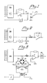
- FIG. 1 shows schematically a previously known stray pulse eliminating device
- an amplifier F1 is connected to the output of a D/A converter DA having current output.
- the output of the amplifier F1 is connected to the input of a second amplifier F2 via a switch S1.
- the input of the second amplifier F2 is connected to a reference level, in this embodiment ground, via a capacitor C.
- the switch S1 is controlled by a prediction circuit P which predicts the time of the occurance of a stray pulse. When a stray pulse is expected to occur the prediction circuit P ensures that the switch S1 disconnects the connection between the amplifiers F1, F2. The signal across the capacitor C at the time of disconnection then remains stored across the capacitor. When the expected stray pulse is assumed to have ceased the switch S1 is reclosed and the capacitor rapidly is charged to a signal value which now is present on the output of the first amplifier F1.
- a device comprises an inductor L, such as a choke coil, connected between the output of the D/A converter and the input of an operational amplifier F and a switch S2 connected between the output of the D/A converter DA and ground.
- the switch S2 is controlled by a prediction circuit P which predicts the time of the occurance of a stray pulse. Just before the pulse is expected to occur the prediction circuit P ensures that the switch S2 is closed and then is maintained closed for a period containing the instant of the occurance of the expected stray pulse. The current from the output of the D/A converter DA then remains stored in the inductor L and the charge of the stray pulse is shortcuited to ground.
- the inductor L is connected between the switch S2 and the summing point of the operational amplifier F the voltage across the inductor L is practically zero. Accordingly, this does not give rise to any significant current change during the period when the switch S2 is closed.
- the switch S2 is reopened the current at the output of the D/A converter DA is supplied to the inductor L which rapidly changes its current to the new value.
- the switch is constituted by a diode and resistor coupling consisting of four diodes and four resistors.
- the diodes which ought to be of a rapid type are arranged in a bridge coupling consisting of two parallel coupling paths with two unidirected diodes D1, D2 and D3, D4, respectively , in each of the coupling paths.
- the junction 1 between the diodes D1, D2 in one of the coupling paths is connected to the output of the D/A converter DA and the junction 2 between the diodes D3, D4 in the other coupling path is connected to ground.
- One of the common ends 3 of the coupling paths is connected to one terminal of the output of a high-frequency transformer TR via a resistor R1 and the other common end 4 of the coupling paths is connected to the other terminal of the output of the highfrequency transformer TR via a resistor R2. Furthermore, a resistor R3 is connected between a terminal of the transformer TR and ground and a further resistor R4 is connected between the other terminal of the transformer TR and ground.
- the switch S1 in the form of a diode and resistor bridge is closed by means of a pulse signal at the output of a driver, for example a TTL gate, being supplied to the resistor and the diode coupling via the high-frequency transformer TR.
- a driver for example a TTL gate
- the signal pulls equal currents through the two coupling paths so that the junctions 1, 2 between the diodes D1, D2 and D3, D4, respectively, in the coupling paths assume substantially the same potential, that is the potential of ground.
- a lowpass filter LP is shown at the output of the amplifier F.
- the filter prevents high frequency signals from passing so that the output of the filter becomes a constant direct current.
- the lowpass filter function is obtained by a system coupled to the output of the amplifier, the system being in the form of, for example, a deflection system having per se a limited band width and hence an upper limiting frequency.
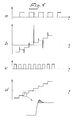
- Fig. 4a-d time diagrams of the device according to the invention are shown.
- the digital input signal of the D/A converter is assumed having been generated by a BCD counter clocked with a constant frequency so that the ideal output current of the D/A converter thus should have an evenly ascending stair-case shape.
- Fig. 4a shows the clock pulses of the counter.
- Fig. 4b shows the D/A converter output current which as shown may have both positive and negative stray pulses of varying amplitudes.
- Fig. 4c indicates the time intervals during which stray pulses are expected to occur, that is the time intervals during which, according to the invention, the switch S2 is maintained closed.
- Fig. 4d shows the actual current through the inductor L at the output of the D/A converter, the upper front edge of a stairstep being shown in an enlarged scale.
- the region of the enlarging having oblique strokes has a substantial constant charge content for each stairstep. Accordingly, the current curve deviates somewhat from the ideal evenly ascending staircase due to transients occurring when the switch S2 is closed, but these disturbances have as has already been pointed out a substantially constant charge content.
Landscapes
- Engineering & Computer Science (AREA)
- Theoretical Computer Science (AREA)
- Analogue/Digital Conversion (AREA)
- Details Of Television Scanning (AREA)
Claims (4)
- Schaltungsanordnung zum Beseitigen von Streuimpulsen am Ausgang eines Digital-Analog-Umsetzers (D/A-Umsetzers), wobei diese Schaltungsanordnung einen mit dem Ausgang des D/A-Umsetzers verbindbaren Eingang sowie einen Ausgang hat und Schaltmittel, Speichermittel und einen Prädiktionskreis aufweist, mit dem die Zeitpunkte, an denen das Auftreten von Streuimpulsen erwartet wird, berechnet und abhängig davon die Schaltmittel aktiviert werden können, wobei ein etwaiger Streuimpuls am Ausgang des D/A-Umsetzers durch die Schaltmittel daran gehindert wird, den Ausgang der Schaltungsanordnung zu erreichen, und zwar während einer Zeit, in der der Impuls auftritt, wobei die Speichermittel mit den Schaltmitteln gekoppelt sind, sowie mit dem Ausgang der Schaltungsanordnung zum Speichern des an dem Ausgang des D/A-Umsetzers während der Zeit, in der die Schaltmittel nicht aktiviert sind, vorhandenen Signals,
dadurch gekennzeichnet, daß der D/A-Umsetzer einen Stromausgang aufweist und die Speichermittel eine zwischen dem Ausgang des D/A-Umsetzers und dem Ausgang der Schaltungsanordnung vorgesehene Induktivität aufweisen, wobei die Schaltmittel zwischen dem Ausgang des D/A-Umsetzers und einem Bezugspotential zum Kurzschließen des Ausgangs des D/A-Umsetzers zu dem Bezugspotential während der Zeitperiode, in der der Impuls auftritt, vorgesehen sind. - Schaltungsanordnung nach Anspruch 1, dadurch gekennzeichnet, daß die Induktivität eine Drosselspule ist.
- Schaltungsanordnung nach einem der vorstehenden Ansprüche, dadurch gekennzeichnet, daß die Schaltmittel eine Diodenkopplung mit zwei parallelen Koppelstrecken mit je zwei reihengeschalteten Sperrdioden aufweisen, wobei der Übergang zwischen den Dioden in der einen Koppelstrecke mit dem Ausgang des Digital-Analog-Umsetzers verbunden ist und der Übergang zwischen den Dioden in der anderen Koppelstrecke mit dem Bezugspotential verbunden ist, sowie ein Widerstandsnetzwerk aus einem ersten Widerstand zwischen der einen Eingangsklemme des Schalters und einem gemeinsamen Übergang der Koppelstrecken, einem zweiten Widerstand zwischen der anderen Eingangsklemme des Schalters und einem zweiten gemeinsamen Übergang der Koppelstrecken, einem dritten Widerstand zwischen der ersten Eingangsklemme und dem Bezugspotential, sowie einem vierten Widerstand zwischen der zweiten Eingangsklemme und dem Bezugspotential.
- Schaltungsanordnung nach Anspruch 3, dadurch gekennzeichnet, daß ein der ersten und zweiten Eingangklemme des Schalters zugeführtes Impulssignal über einen Transformator gekoppelt wird.
Applications Claiming Priority (2)
| Application Number | Priority Date | Filing Date | Title |
|---|---|---|---|
| SE8304290 | 1983-08-05 | ||
| SE8304290A SE437750B (sv) | 1983-08-05 | 1983-08-05 | Anordning for eliminering av storpulser pa utgangen av en d/a-omvandlare |
Publications (3)
| Publication Number | Publication Date |
|---|---|
| EP0136739A2 EP0136739A2 (de) | 1985-04-10 |
| EP0136739A3 EP0136739A3 (en) | 1987-10-21 |
| EP0136739B1 true EP0136739B1 (de) | 1992-03-11 |
Family
ID=20352126
Family Applications (1)
| Application Number | Title | Priority Date | Filing Date |
|---|---|---|---|
| EP84201130A Expired - Lifetime EP0136739B1 (de) | 1983-08-05 | 1984-08-01 | Streuimpulsbeseitigungsvorrichtung für einen DA-Wandler |
Country Status (4)
| Country | Link |
|---|---|
| US (1) | US4638301A (de) |
| EP (1) | EP0136739B1 (de) |
| DE (1) | DE3485557D1 (de) |
| SE (1) | SE437750B (de) |
Families Citing this family (1)
| Publication number | Priority date | Publication date | Assignee | Title |
|---|---|---|---|---|
| US4825448A (en) * | 1986-08-07 | 1989-04-25 | International Mobile Machines Corporation | Subscriber unit for wireless digital telephone system |
Family Cites Families (2)
| Publication number | Priority date | Publication date | Assignee | Title |
|---|---|---|---|---|
| GB1385410A (en) * | 1972-08-10 | 1975-02-26 | Micro Consultants Ltd | Signal sampling |
| US4132908A (en) * | 1977-08-04 | 1979-01-02 | Smiths Industries, Inc. | Digital-to-analog conversion with deglitch |
-
1983
- 1983-08-05 SE SE8304290A patent/SE437750B/sv not_active IP Right Cessation
-
1984
- 1984-08-01 DE DE8484201130T patent/DE3485557D1/de not_active Expired - Lifetime
- 1984-08-01 EP EP84201130A patent/EP0136739B1/de not_active Expired - Lifetime
- 1984-08-06 US US06/638,135 patent/US4638301A/en not_active Expired - Fee Related
Non-Patent Citations (1)
| Title |
|---|
| U Tietze/CH Schenk: "Halbleiter-Schaltungstechnik", 5th edition, Springer-Verlag Berlin Heidelberg New York, 1980, pp 399-400; "Sourcebook of Electronic Circuits", McGraw-Hill Inc 1980, p.82 * |
Also Published As
| Publication number | Publication date |
|---|---|
| EP0136739A3 (en) | 1987-10-21 |
| SE8304290L (de) | 1985-02-06 |
| SE437750B (sv) | 1985-03-11 |
| DE3485557D1 (de) | 1992-04-16 |
| SE8304290D0 (sv) | 1983-08-05 |
| EP0136739A2 (de) | 1985-04-10 |
| US4638301A (en) | 1987-01-20 |
Similar Documents
| Publication | Publication Date | Title |
|---|---|---|
| EP0135212B1 (de) | Band-Sperr-Filter mit geschalteten Kapazitäten | |
| US4531096A (en) | Pulse-width modulation circuit | |
| US4349703A (en) | Programmable ring signal generator | |
| GB2222044A (en) | Isolation amplifier | |
| GB1585890A (en) | Gating circuits for semiconductors | |
| US3976942A (en) | Watt/watt hour transducer having current signals and a modulator therefor | |
| JPH09511633A (ja) | パルスカウントfm復調器を具える受信機、及びパルスカウントfm復調器 | |
| EP0351009B1 (de) | Schleifenstromreguliereinrichtung für eine Fernsprechleitung | |
| US4500844A (en) | Ringing signal generator employing delta-modulation power amplification techniques | |
| EP0029067B1 (de) | Umrichteranordnung zum Speichern eines vorbestimmten Energiemenge | |
| CA1123067A (en) | Variable leading edge circuit apparatus | |
| EP0136739B1 (de) | Streuimpulsbeseitigungsvorrichtung für einen DA-Wandler | |
| US4652774A (en) | Rectangular wave-shaping circuit with varying threshold level | |
| CA2037944C (en) | Switching converter | |
| US4425515A (en) | Method and means to minimize risetime of a microwave pulse modulated signal from a frequency multiplier circuit | |
| US4354062A (en) | Communication system signaling circuit | |
| JPH0683332B2 (ja) | 電信電話装置における加入者接続―端末装置への電力遠隔供給のための回路設備 | |
| SU1429948A3 (ru) | Статический счетчик киловатт-часов | |
| US5097229A (en) | Modulator - demodulator transformer coupled d.c. to one mhz information channel | |
| US3783304A (en) | Constant pulse width generator | |
| US4290034A (en) | Switched capacitor filter | |
| EP0367522A2 (de) | Impulsbreiten-Analog/Digitalwandler mit geschlossener Schleife | |
| US4247823A (en) | Low noise, low phase shift analog signal multiplier | |
| US4594578A (en) | One shot pulse width modulating converter | |
| US4550308A (en) | Signal converting apparatus |
Legal Events
| Date | Code | Title | Description |
|---|---|---|---|
| PUAI | Public reference made under article 153(3) epc to a published international application that has entered the european phase |
Free format text: ORIGINAL CODE: 0009012 |
|
| AK | Designated contracting states |
Designated state(s): DE FR GB SE |
|
| PUAL | Search report despatched |
Free format text: ORIGINAL CODE: 0009013 |
|
| AK | Designated contracting states |
Kind code of ref document: A3 Designated state(s): DE FR GB SE |
|
| 17P | Request for examination filed |
Effective date: 19880418 |
|
| 17Q | First examination report despatched |
Effective date: 19890818 |
|
| GRAA | (expected) grant |
Free format text: ORIGINAL CODE: 0009210 |
|
| AK | Designated contracting states |
Kind code of ref document: B1 Designated state(s): DE FR GB SE |
|
| REF | Corresponds to: |
Ref document number: 3485557 Country of ref document: DE Date of ref document: 19920416 |
|
| ET | Fr: translation filed | ||
| PLBE | No opposition filed within time limit |
Free format text: ORIGINAL CODE: 0009261 |
|
| STAA | Information on the status of an ep patent application or granted ep patent |
Free format text: STATUS: NO OPPOSITION FILED WITHIN TIME LIMIT |
|
| 26N | No opposition filed | ||
| EAL | Se: european patent in force in sweden |
Ref document number: 84201130.6 |
|
| REG | Reference to a national code |
Ref country code: FR Ref legal event code: CD |
|
| PGFP | Annual fee paid to national office [announced via postgrant information from national office to epo] |
Ref country code: GB Payment date: 19950731 Year of fee payment: 12 |
|
| PGFP | Annual fee paid to national office [announced via postgrant information from national office to epo] |
Ref country code: SE Payment date: 19950825 Year of fee payment: 12 |
|
| PGFP | Annual fee paid to national office [announced via postgrant information from national office to epo] |
Ref country code: FR Payment date: 19950830 Year of fee payment: 12 |
|
| PGFP | Annual fee paid to national office [announced via postgrant information from national office to epo] |
Ref country code: DE Payment date: 19951024 Year of fee payment: 12 |
|
| PG25 | Lapsed in a contracting state [announced via postgrant information from national office to epo] |
Ref country code: GB Effective date: 19960801 |
|
| PG25 | Lapsed in a contracting state [announced via postgrant information from national office to epo] |
Ref country code: SE Effective date: 19960802 |
|
| GBPC | Gb: european patent ceased through non-payment of renewal fee |
Effective date: 19960801 |
|
| PG25 | Lapsed in a contracting state [announced via postgrant information from national office to epo] |
Ref country code: FR Effective date: 19970430 |
|
| PG25 | Lapsed in a contracting state [announced via postgrant information from national office to epo] |
Ref country code: DE Effective date: 19970501 |
|
| EUG | Se: european patent has lapsed |
Ref document number: 84201130.6 |
|
| REG | Reference to a national code |
Ref country code: FR Ref legal event code: ST |