EP0134069B1 - Bipolar transistor having a heterojunction between base and collector - Google Patents
Bipolar transistor having a heterojunction between base and collector Download PDFInfo
- Publication number
- EP0134069B1 EP0134069B1 EP84302952A EP84302952A EP0134069B1 EP 0134069 B1 EP0134069 B1 EP 0134069B1 EP 84302952 A EP84302952 A EP 84302952A EP 84302952 A EP84302952 A EP 84302952A EP 0134069 B1 EP0134069 B1 EP 0134069B1
- Authority
- EP
- European Patent Office
- Prior art keywords
- region
- collector
- base
- heterojunction
- semiconductor material
- Prior art date
- Legal status (The legal status is an assumption and is not a legal conclusion. Google has not performed a legal analysis and makes no representation as to the accuracy of the status listed.)
- Expired
Links
- 230000007704 transition Effects 0.000 claims description 46
- 239000000463 material Substances 0.000 claims description 29
- 239000004065 semiconductor Substances 0.000 claims description 26
- 229910001218 Gallium arsenide Inorganic materials 0.000 claims description 11
- 230000004888 barrier function Effects 0.000 claims description 11
- 239000000203 mixture Substances 0.000 claims description 5
- 239000000370 acceptor Substances 0.000 claims description 4
- 230000005684 electric field Effects 0.000 description 17
- 239000012535 impurity Substances 0.000 description 11
- 239000002131 composite material Substances 0.000 description 8
- 238000000034 method Methods 0.000 description 6
- 238000001451 molecular beam epitaxy Methods 0.000 description 6
- 239000000758 substrate Substances 0.000 description 6
- 230000008569 process Effects 0.000 description 5
- XUIMIQQOPSSXEZ-UHFFFAOYSA-N Silicon Chemical compound [Si] XUIMIQQOPSSXEZ-UHFFFAOYSA-N 0.000 description 4
- 239000000969 carrier Substances 0.000 description 4
- 230000008859 change Effects 0.000 description 4
- 238000009826 distribution Methods 0.000 description 4
- 229910052710 silicon Inorganic materials 0.000 description 4
- 239000010703 silicon Substances 0.000 description 4
- 230000000694 effects Effects 0.000 description 3
- 230000010354 integration Effects 0.000 description 3
- 229910052790 beryllium Inorganic materials 0.000 description 2
- ATBAMAFKBVZNFJ-UHFFFAOYSA-N beryllium atom Chemical compound [Be] ATBAMAFKBVZNFJ-UHFFFAOYSA-N 0.000 description 2
- 230000003247 decreasing effect Effects 0.000 description 2
- 238000003860 storage Methods 0.000 description 2
- 230000015572 biosynthetic process Effects 0.000 description 1
- 238000005229 chemical vapour deposition Methods 0.000 description 1
- 239000013078 crystal Substances 0.000 description 1
- 230000007423 decrease Effects 0.000 description 1
- 238000005421 electrostatic potential Methods 0.000 description 1
- 238000004519 manufacturing process Methods 0.000 description 1
- 230000000717 retained effect Effects 0.000 description 1
Images


Classifications
-
- H—ELECTRICITY
- H10—SEMICONDUCTOR DEVICES; ELECTRIC SOLID-STATE DEVICES NOT OTHERWISE PROVIDED FOR
- H10D—INORGANIC ELECTRIC SEMICONDUCTOR DEVICES
- H10D48/00—Individual devices not covered by groups H10D1/00 - H10D44/00
- H10D48/30—Devices controlled by electric currents or voltages
- H10D48/32—Devices controlled by only the electric current supplied, or only the electric potential applied, to an electrode which does not carry the current to be rectified, amplified or switched
- H10D48/34—Bipolar devices
- H10D48/345—Bipolar transistors having ohmic electrodes on emitter-like, base-like, and collector-like regions
-
- H—ELECTRICITY
- H10—SEMICONDUCTOR DEVICES; ELECTRIC SOLID-STATE DEVICES NOT OTHERWISE PROVIDED FOR
- H10D—INORGANIC ELECTRIC SEMICONDUCTOR DEVICES
- H10D10/00—Bipolar junction transistors [BJT]
- H10D10/80—Heterojunction BJTs
- H10D10/821—Vertical heterojunction BJTs
Definitions
- This invention relates to a heterojunction semiconductor device and, more particularly, to a bipolar transistor provided with a heterojunction formed between base and collector regions.
- the heterojunction bipolar transistor is known to offer more advantages than the conventional homojunction transistor made of a single semiconductor material. These advantages may be broadly classified into those realized by forming a heterojunction between emitter and base regions of a transistor and those derived from providing a heterojunction between base and collector regions of the transistor.
- the so-called wide-gap emitter structure obtained by forming a heterojunction between the emitter and base regions of the transistor offers the following advantages:
- a wide-gap collector structure obtained by preparing a collector region from a material having a broader energy gap than the base region has the following advantages:
- the heterojunction bipolar transistor having the above-mentioned merits has been found to be far more excellent than the conventional homojunction bipolar transistor in respect of its high frequency and switching characteristics.
- an energy barrier ⁇ Ec is produced in the conduction band in the heterojunction.
- the occurrence of the energy barrier ⁇ Ec arises from the discontinuity of the conduction band.
- the energy barrier ⁇ Ec obstructs the transport of electrons from the emitter region to the collector region. This fact eventually leads to a decline in the transport factor of the base region and to the loss of the DC characteristic of the transistor.
- the DC characteristic can be effectively prevented from falling by adopting a grading layer structure allowing energy gaps to slowly vary from the base region to the collector region, instead of providing an abrupt heterojunction between the base and collector regions. This is because the barrier in the conduction band has a smaller height than that of the abrupt heterojunction.
- transition region The region in which the energy gap varies from the collector region to the base region.
- an object of this invention to provide a heterojunction bipolar transistor of a wide-gap collector structure having improved DC charactersitics.
- a heterojunction bipolar transistor of this invention comprises: an n-type emitter region; a p-type base region comprising a region which is formed of a first kind of semiconductor material and defines the pn junction with the emitter region; and a n-type collector region which is formed of a second kind of semiconductor material and defines a heterojunction with the base region, the collector region having a wider energy gap than the base region and producing an energy barrier AEc[eV] in the conduction band in the heterojunction, a transition region having a thickness Wt [cm] is formed in the heterojunction defined between the base region and collector region wherein the semiconductor material composition gradually varies, and the energy gap varies, said transition region being included in a depletion layer which is formed by a built-in voltage said transition region extending over at least said base region (114), between said base region and collector region, and the relationship between said energy barrier ⁇ Ec and the width Wt (cm) of said transition region being given by
- the heterojunction bipolar transistor of this invention constructed as described above has improved DC characteristics as well as advantages offered by the wide gap collector structure.
- the subject heterojunction bipolar transistor stands above conventional homojunction bipolar transistors in respect of its high frequency and switching characteristics.
- a heterojunction bipolar transistor embodying this invention uses a wide energy gap region as a collector region and a narrow energy gap region as a base region.
- the narrow energy gap region is of p-type and the wide energy gap region is of n-type. Then the conduction band and valence band have their profiles changed from those of Fig. 1 to those of Fig. 2 due to the redistribution of the electric charge resulting from the formation of the pn junction.
- Fig. 2 shows the condition of the conduction band and valence band when the pn junction is depleted due to the effect of inverse voltage or built-in voltage.
- the origin of the position coordinate x is chosen to the position of the pn junction.
- the position coordinate is defined as positive in the direction of the wide energy gap region.
- Wnd denotes the edge of depletion layer formed at the collector region
- -Wpd represents the edge of depletion layer formed at the base region.
- -Wpt denotes the base-side edge of the transition region where the energy gap slowly varies
- Wnt the collector-side edge of the transition region.
- a transition region is generally formed by progressively varying, over the range extending from the base region to the collector region, the mixed-crystal ratio between the first kind of semiconductor material forming the base region and the second kind of semiconductor material forming the collector region.
- the process of molecular beam epitaxy is used for forming the transition region, it is most facile to linearly change the mixing ratio with respect to the position x.
- the shape of the condition band may be considered to change approximately linearly from the narrow energy gap region to the wide energy gap region. Therefore, the following equation (10) results: where:
- AEc the barrier height (measured in the unit of eV) in the conduction band when the wide energy gap collector and the narrow energy gap base are connected together without an intervening transition region (the total width of the transition region).
- an electric field E(x) acting on electrons moving from the emitter region to the collector region is expressed by the sum of equations (8) and (10).
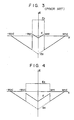
- This composite electric field E(x) is indicated by the solid lines shown in Fig. 3.
- the broken line given in Fig. 3 denotes the electric field Ee expressed by equation (8).
- the one dot-dash line represents the electric field Es expressed by equation (10).
- the composite electric field E(x) should have a negative maximum value. If the transition region extends beyond the depletion region, it will be evident that a region in which the composite electric field E(x) becomes positive appears, since the electric field Es is positive. Therefore, the first requisite condition of a heterojunction bipolar transistor embodying this invention is that a transition region defined between the base and collector regions should be included in the depletion layer which is produced when a prescribed inverse voltage is impressed between the base and collector regions.
- a composite electric field E(x) obtained on the collector side is expressed as follows:
- Equation (13) The condition that E of equation (13) is negative is necessary for electrons injected from the emitter region to reach the collector region without undergoing a repulsive force. Eventually, therefore, the. necessary condition for suppressing a drop in the transport factor of the base region may be given by
- the integration of the right side of equation (14) is equal to the total amount r2 of the effective donors present in that portion of the collector-side depletion layer which is not included in the transition region. Therefore,
- Equations (15), (16) represent a second requisite condition necessary to realize the heterojunction bipolar transistor of this invention.
- the elements included in equations (15), (16) are measured in the following units:
- the aforementioned first and second requisite conditions of the subject heterojunction bipolar transistor define the upper and lower limits of the width Wt of the transition region. This will be discussed more practically hereinafter.
- a heterojunction bipolar transistor embodying this invention which prepares a wider-gap semiconductor material from Ga 1 _ x AI x As and a narrow-gap semiconductor material from GaAs.
- n +- type GaAs substrate 110 Formed on an n +- type GaAs substrate 110 is a collector region 112 formed of n-type Ga 1 _ x AI x As.
- a base region 114 of p-type GaAs Formed on the base region 114 is an n-type emitter region 116 prepared from Ga 1 _ x AI x As.
- the GaAs substrate 110 is contacted by an electrode 118, and the emitter region 116 is contacted by an electrode 120.
- a transition region 122 having a width Wt is provided to extend over the collector region 112 and the base region 114. The transition region 122 is formed so as to satisfy equations (1) and (2).
- GaAs is the optimum material for the substrate 110.
- the molecular beam epitaxy (MBE) process may be considered as acceptable in forming a transistor on the substrate 110. When the compositions of the various materials must be precisely controlled as in the structure of this invention, the MBE process proves most satisfactory.
- the flow rate of Ga, As and Al must be controlled and an impurity, for example, Si, should be introduced during the growth. Further, the flow rate of AI must also be controlled in the growth of the transition region 122 extending from the collector region 112 into the base region 114 in order to effect the slow change of the composition from Ga 1 _x AI x As to GaAs. In this case, the flow rate of AI has to be precisely controlled. In the embodiment of this invention, however, the thickness of the transition region 122 is more than several scores nm (several hundred Angstrom) units as described later.
- the application of the MBE process ensures the control of the above-mentioned AI flow rate.
- the collector region 112 of Ga 1 _ x AI x As the energy gap changes substantially in proportion to the value of x which is less than 0.3. Therefore, by varying the flow rate of AI in proportion to the growth time, it is possible to form the transition region 122 wherein the energy gap varies substantially linearly.
- the p-type base region 114 of GaAs is formed similarly by the MBE process with Be, for example, used as the impurity.
- the n-type emitter region 116 is produced by the growth of Ga 1 _ x AI x As while introducing an n-type impurity of silicon.
- the transition region 122 is formed in the collector region 112 and into the base region 114 and is doped into n-type with the silicon impurity concentration of 3x10 16 c m - 3 .
- equation (1) may be rewritten as follows: Therefore, the requisite condition for the width Wt may be expressed as follows: Considering the dielectric constant of the transition region 122 to have a value fully approaching that of the collector region 112, and using the absolute depletion layer approximation, the following relation results: where:
- Fig. 6 of a heterojunction bipolar transistor according to a second embodiment of the invention.
- the transition region 122 having the width Wt is formed in the base region 114 alone.
- the other parts of the second embodiment of Fig. 6 are the same as those of the first embodiment of Fig. 5 and are denoted by the same numerals.
- the transition region 122 is so formed as to satisfy equations (1), (2). This second embodiment ensures a high speed operation without losing the DC characteristics as in the first embodiment of Fig. 5.
Landscapes
- Bipolar Transistors (AREA)
Description
- This invention relates to a heterojunction semiconductor device and, more particularly, to a bipolar transistor provided with a heterojunction formed between base and collector regions.
- Recently, a noticeable development has been made in the heterojunction semiconductor devices constructed by bonding together different kinds of semiconductor materials due to the progress in molecular beam epitaxy (MBE) or in metal-organic chemical vapor deposition (MOCVD). The heterojunction bipolar transistor is known to offer more advantages than the conventional homojunction transistor made of a single semiconductor material. These advantages may be broadly classified into those realized by forming a heterojunction between emitter and base regions of a transistor and those derived from providing a heterojunction between base and collector regions of the transistor. The so-called wide-gap emitter structure obtained by forming a heterojunction between the emitter and base regions of the transistor offers the following advantages:
- a1: The emitter efficiency can be elevated, even if the impurity concentration of the emitter region bears a small ratio to that of the base region.
- a2: Since the base region is allowed to have a large impurity concentration, the base resistance can be reduced.
- a3: Since the emitter region is allowed to have a small impurity concentration, the emitter capacitance can be decreased.
- On the other hand, a wide-gap collector structure obtained by preparing a collector region from a material having a broader energy gap than the base region has the following advantages:
- b1: Since, in the saturation region, minority carriers are prevented from being injected from the base region into the collector region, the storage region for the excess carriers can be reduced in size.
- b2: When minority carriers are prominently injected, the base push-out effect is restricted, thereby enabling the storage region for the excess carriers to be decreased in size.
- The heterojunction bipolar transistor having the above-mentioned merits has been found to be far more excellent than the conventional homojunction bipolar transistor in respect of its high frequency and switching characteristics. However, if in the case of an npn transistor having a wide-gap collector structure, an abrupt heterojunction is formed by directly connecting the wide-gap collector to the base region, then an energy barrier ΔEc is produced in the conduction band in the heterojunction. The occurrence of the energy barrier ΔEc arises from the discontinuity of the conduction band. The energy barrier ΔEc obstructs the transport of electrons from the emitter region to the collector region. This fact eventually leads to a decline in the transport factor of the base region and to the loss of the DC characteristic of the transistor. The DC characteristic can be effectively prevented from falling by adopting a grading layer structure allowing energy gaps to slowly vary from the base region to the collector region, instead of providing an abrupt heterojunction between the base and collector regions. This is because the barrier in the conduction band has a smaller height than that of the abrupt heterojunction.
- The energy barrier ΔEc in the grading layer structure has already been discussed in various treatises, for example, in "Heterostructure Bipolar Transistors and Integrated Circuits" by H. Kroemer, Proceedings of the IEEE, vol. 70, No. 1, pp. 13-25, January, 1982 and in "A Simplified Model for Graded-Gap Heterojunctions" by D. T. Cheung et al, Solid-State Electronics, vol. 18, pp. 263-266, 1975. However, the publications known to date have given no clear hints as to what condition should be retained by a region in which the energy gap varies from the collector region to the base region.
- The region in which the energy gap varies from the collector region to the base region is referred to as "transition region" hereinafter.
- It is, accordingly, an object of this invention to provide a heterojunction bipolar transistor of a wide-gap collector structure having improved DC charactersitics.
- To attain the above-mentioned object, a heterojunction bipolar transistor of this invention comprises: an n-type emitter region; a p-type base region comprising a region which is formed of a first kind of semiconductor material and defines the pn junction with the emitter region; and a n-type collector region which is formed of a second kind of semiconductor material and defines a heterojunction with the base region, the collector region having a wider energy gap than the base region and producing an energy barrier AEc[eV] in the conduction band in the heterojunction, a transition region having a thickness Wt [cm] is formed in the heterojunction defined between the base region and collector region wherein the semiconductor material composition gradually varies, and the energy gap varies, said transition region being included in a depletion layer which is formed by a built-in voltage said transition region extending over at least said base region (114), between said base region and collector region, and the relationship between said energy barrier ΔEc and the width Wt (cm) of said transition region being given by:-


- q=elementary charge [C]
- e1=dielectric constant [Farad/cm] of the first kind of semiconductor material
- e2=dielectric constant [Farad/cm] of the second kind of semiconductor material
- Γ1=total amount of effective acceptors in that portion of the base side depletion layer which is not included in the transition region
- r2=total amount of the effective donors in that portion of the collector side depletion layer which is not included in the transition region.
- The heterojunction bipolar transistor of this invention constructed as described above has improved DC characteristics as well as advantages offered by the wide gap collector structure. The subject heterojunction bipolar transistor stands above conventional homojunction bipolar transistors in respect of its high frequency and switching characteristics.
- The objects and advantages of this invention will be apparent from the following description taken in conjunction with the accompanying drawings, in which:
- Fig. 1 illustrates the energy band profile of a heterojunction having a transition region, with no consideration given to the redistribution of electric charges;
- Fig. 2 shows an energy band profile of a heterojunction having a transition region with the redistribution of the electric charges taken into account;
- Fig. 3 shows the distribution of an electric field in the depletion layer of a heterojunction having a conventional transition region;
- Fig. 4 indicates the distribution of an electric field in the depletion layer of a heterojunction having a transition region embodying this invention; and
- Figs. 5 and 6 are cross-sectional views of heterojunction bipolar transistors according to embodiments of this invention.
- If two kinds of semiconductor materials are connected so as to provide a transition region between the materials, and the redistribution of electric charges between these semiconductor materials is not taken into account, then an energy band as shown in Fig. 1 is obtained with respect to the position coordinate x due to the differences between the
electron affinities - A detailed description may now be made, with reference to Fig. 2, of a heterojunction bipolar transistor embodying this invention. Now consider the potential ψ expressed by equation (3) which equivalently represents the shape of a conduction band.

- Ec(x)=energy of the conduction band
- q=electric elementary charge
- ψ(x) denotes the sum of electrostatic potential ψe(x) resulting from the distribution of electric charge and potential ψs(x) caused by changes in the band structure.
- Thus,


- e(x)=the dielectric constant of a semiconductor material at the position x
- Nd(x), Na(x)=the respective densities of ionized donors and acceptors.
- Ee(x)=0 is obtained in each of the following conditions:


- Now, let it be assumed an electric field corresponding to the potential ψs(x) resulting from changes in band structure is expressed as follows:


- AEc=the barrier height (measured in the unit of eV) in the conduction band when the wide energy gap collector and the narrow energy gap base are connected together without an intervening transition region

- In an npn transistor having a heterojunction with a transition region formed between the base and collector regions, an electric field E(x) acting on electrons moving from the emitter region to the collector region is expressed by the sum of equations (8) and (10). This composite electric field E(x) is indicated by the solid lines shown in Fig. 3. The broken line given in Fig. 3 denotes the electric field Ee expressed by equation (8). The one dot-dash line represents the electric field Es expressed by equation (10). When the composite electric field E(x) has a positive value, electrons are pushed back toward the emitter by the electric field. When, therefore, electrons injected from the emitter into the base region has to reach the collector region without undergoing a repulsive force, the composite electric field E(x) should have a negative maximum value. If the transition region extends beyond the depletion region, it will be evident that a region in which the composite electric field E(x) becomes positive appears, since the electric field Es is positive. Therefore, the first requisite condition of a heterojunction bipolar transistor embodying this invention is that a transition region defined between the base and collector regions should be included in the depletion layer which is produced when a prescribed inverse voltage is impressed between the base and collector regions.
- When the transition region is included in the depletion region, a composite electric field E(x) obtained on the collector side is expressed as follows:

 of equation (13) is negative is necessary for electrons injected from the emitter region to reach the collector region without undergoing a repulsive force. Eventually, therefore, the. necessary condition for suppressing a drop in the transport factor of the base region may be given by


- If the same discussion as described above is applied to the base region, then

- e1=the dielectric constant of the first kind of semiconductor material forming the base region
-
Γ 1 =the total amount of effective acceptors present in that portion of the base side depletion layer extending from the pn junction to the base region which is not included in the transition region. - Equations (15), (16) represent a second requisite condition necessary to realize the heterojunction bipolar transistor of this invention. The elements included in equations (15), (16) are measured in the following units:
- AEc=the unit of [eV]
- Wt=the unit of [cm]
- q=the unit of [C] or Coulomb
- e1 and s2=the unit of [Farad/cm].
- The aforementioned first and second requisite conditions of the subject heterojunction bipolar transistor define the upper and lower limits of the width Wt of the transition region. This will be discussed more practically hereinafter.
- For the convenience of discussion, let it be assumed that the effective donor density of the collector side is fixed. Then equation (15) may be rewritten as follows:


- AEcn=the barrier height in the conduction band when a stepped heterojunction is formed between a semiconductor material having the composition of the pn junction and the semiconductor material forming the collector region.
- The following equation is derived from equations (17) and (18):


- A description may now be made, with reference to Fig. 5, of a heterojunction bipolar transistor embodying this invention which prepares a wider-gap semiconductor material from Ga1_xAIxAs and a narrow-gap semiconductor material from GaAs. Formed on an n+-
type GaAs substrate 110 is acollector region 112 formed of n-type Ga1_xAIxAs. Formed on thecollector region 112 is abase region 114 of p-type GaAs. Formed on thebase region 114 is an n-type emitter region 116 prepared from Ga1_xAIxAs. TheGaAs substrate 110 is contacted by anelectrode 118, and theemitter region 116 is contacted by anelectrode 120. Atransition region 122 having a width Wt is provided to extend over thecollector region 112 and thebase region 114. Thetransition region 122 is formed so as to satisfy equations (1) and (2). - A description may now be made of the method of manufacturing the heterojunction bipolar transistor. To fabricate such a bipolar transistor it is necessary to epitaxially grow the
collector region 112, thebase region 114 and theemitter region 116 on the electrically conducting orsemi-insulating substrate 110 successively. In this embodiment, where Ga,_xAlxAs is used as a collector material, GaAs is the optimum material for thesubstrate 110. The molecular beam epitaxy (MBE) process may be considered as acceptable in forming a transistor on thesubstrate 110. When the compositions of the various materials must be precisely controlled as in the structure of this invention, the MBE process proves most satisfactory. When thecollector region 112 of the n-type Ga1_xAIxAs is grown on theGaAs substrate 110, the flow rate of Ga, As and Al must be controlled and an impurity, for example, Si, should be introduced during the growth. Further, the flow rate of AI must also be controlled in the growth of thetransition region 122 extending from thecollector region 112 into thebase region 114 in order to effect the slow change of the composition from Ga1_xAIxAs to GaAs. In this case, the flow rate of AI has to be precisely controlled. In the embodiment of this invention, however, the thickness of thetransition region 122 is more than several scores nm (several hundred Angstrom) units as described later. Therefore, the application of the MBE process ensures the control of the above-mentioned AI flow rate. Further, referring to thecollector region 112 of Ga1_xAIxAs, the energy gap changes substantially in proportion to the value of x which is less than 0.3. Therefore, by varying the flow rate of AI in proportion to the growth time, it is possible to form thetransition region 122 wherein the energy gap varies substantially linearly. The p-type base region 114 of GaAs is formed similarly by the MBE process with Be, for example, used as the impurity. The n-type emitter region 116 is produced by the growth of Ga1_xAIxAs while introducing an n-type impurity of silicon. - A concrete description may now be made of the method of designing the width Wt of the
transition region 122 when thecollector region 112 is prepared from Ga0.7Al0.3As containing a silicon impurity concentration of Nd=3x1016 cm-3 and when thebase region 114 is formed of GaAs containing a beryllium impurity concentration of Na=1X1018 cm-3. As seen from Fig. 5, thetransition region 122 is formed in thecollector region 112 and into thebase region 114 and is doped into n-type with the silicon impurity concentration of 3x1016 cm-3. - Since, in this case, equation (2) is automatically satisfied when equation (1) is satisfied, it suffices to take equation (1) alone into account. In this case, equation (1) may be rewritten as follows:


transition region 122 to have a value fully approaching that of thecollector region 112, and using the absolute depletion layer approximation, the following relation results:
- V=the prescribed reverse voltage applied between the
base region 114 andcollector region 112 - - Vbi=the built-in voltage between the
base region 114 andcollector region 112. - This voltage Vbi is expressed as follows:

- X1, X2=the respective electron affinities [eV] in the
base region 114 andcollector region 112 - Eg1=the energy gap [eV] in the
base region 114 - Nv1=the effective density [cm-3] of the valence band of the
base region 114 - k=Boltzmann's constant
- T=absolute temperature.
- As seen from equation (23), the width Wnd is progressively widened as the reverse voltage V impressed between the
base region 114 andcollector region 112 is increased. As a result, a large lattitude is allowed in designing the width Wt expressed by equation (22). In the actual design, therefore, it is sufficient to set the width of the transition region at Wt as defined by equation (22) where V=0. When V=0 and T=300°K, substituting concrete numerical values into equations (22), (23) and (24) yields: - Vbip=1.52 [V]
- Wnd≈2.55x10⁻⁵ [cm]
- Thus, the design condition for the width Wt is given by
- Therefore, the npn heterojunction bipolar transistor, which comprises the
collector region 112 of Ga0,7Alo,3As containing the silicon impurity concentration of Nd=3x10'6 cm-3 and thebase region 114 of GaAs containing the beryllium impurity concentration of Na=1 X 1018 cm-3, can be operated at a high speed without losing its DC characteristics, if the width of thetransition region 122 falls within the range expressed by equation (25). - A description may now be made with reference to Fig. 6 of a heterojunction bipolar transistor according to a second embodiment of the invention. With this second embodiment, the
transition region 122 having the width Wt is formed in thebase region 114 alone. The other parts of the second embodiment of Fig. 6 are the same as those of the first embodiment of Fig. 5 and are denoted by the same numerals. With the second embodiment of Fig. 6, too, thetransition region 122 is so formed as to satisfy equations (1), (2). This second embodiment ensures a high speed operation without losing the DC characteristics as in the first embodiment of Fig. 5.



Claims (2)


Applications Claiming Priority (2)
| Application Number | Priority Date | Filing Date | Title |
|---|---|---|---|
| JP86071/83 | 1983-05-17 | ||
| JP58086071A JPS59211267A (en) | 1983-05-17 | 1983-05-17 | Hetero junction bipolar transistor |
Publications (3)
| Publication Number | Publication Date |
|---|---|
| EP0134069A2 EP0134069A2 (en) | 1985-03-13 |
| EP0134069A3 EP0134069A3 (en) | 1986-12-30 |
| EP0134069B1 true EP0134069B1 (en) | 1990-03-21 |
Family
ID=13876469
Family Applications (1)
| Application Number | Title | Priority Date | Filing Date |
|---|---|---|---|
| EP84302952A Expired EP0134069B1 (en) | 1983-05-17 | 1984-05-02 | Bipolar transistor having a heterojunction between base and collector |
Country Status (3)
| Country | Link |
|---|---|
| EP (1) | EP0134069B1 (en) |
| JP (1) | JPS59211267A (en) |
| DE (1) | DE3481746D1 (en) |
Families Citing this family (9)
| Publication number | Priority date | Publication date | Assignee | Title |
|---|---|---|---|---|
| JP2647824B2 (en) * | 1984-08-10 | 1997-08-27 | 三洋電機株式会社 | Semiconductor laminated structure |
| GB2181299B (en) * | 1985-09-30 | 1989-03-15 | Gen Electric Plc | Semiconductor devices |
| US4788579A (en) * | 1985-09-30 | 1988-11-29 | The General Electric Company | Semiconductor superlattice |
| CA1299771C (en) * | 1987-02-06 | 1992-04-28 | Tadao Ishibashi | Heterojunction bipolar transistor with collector buffer layer |
| EP0355464A3 (en) * | 1988-08-15 | 1990-04-18 | Motorola, Inc. | Heterojunction bipolar transistor formed on a critically misoriented substrate |
| JP2801624B2 (en) * | 1988-12-09 | 1998-09-21 | 株式会社東芝 | Heterojunction bipolar transistor |
| US5162243A (en) * | 1991-08-30 | 1992-11-10 | Trw Inc. | Method of producing high reliability heterojunction bipolar transistors |
| JP2731089B2 (en) * | 1991-10-02 | 1998-03-25 | 三菱電機株式会社 | High speed operation semiconductor device and method of manufacturing the same |
| DE102008044069B3 (en) | 2008-11-26 | 2010-08-05 | Airbus Deutschland Gmbh | Shaped body for producing a fiber composite component |
Family Cites Families (4)
| Publication number | Priority date | Publication date | Assignee | Title |
|---|---|---|---|---|
| JPS5511329A (en) * | 1978-07-08 | 1980-01-26 | Shunpei Yamazaki | Semiconductor device |
| JPS5511330A (en) * | 1978-07-08 | 1980-01-26 | Shunpei Yamazaki | Semiconductor device having continuous junction |
| DE2847451C2 (en) * | 1978-11-02 | 1986-06-12 | Telefunken electronic GmbH, 7100 Heilbronn | Semiconductor device and method of manufacturing |
| DE3380047D1 (en) * | 1982-09-17 | 1989-07-13 | France Etat | Ballistic heterojunction bipolar transistor |
-
1983
- 1983-05-17 JP JP58086071A patent/JPS59211267A/en active Granted
-
1984
- 1984-05-02 EP EP84302952A patent/EP0134069B1/en not_active Expired
- 1984-05-02 DE DE8484302952T patent/DE3481746D1/en not_active Expired - Lifetime
Also Published As
| Publication number | Publication date |
|---|---|
| DE3481746D1 (en) | 1990-04-26 |
| EP0134069A3 (en) | 1986-12-30 |
| JPH0315353B2 (en) | 1991-02-28 |
| EP0134069A2 (en) | 1985-03-13 |
| JPS59211267A (en) | 1984-11-30 |
Similar Documents
| Publication | Publication Date | Title |
|---|---|---|
| US5060031A (en) | Complementary heterojunction field effect transistor with an anisotype N+ ga-channel devices | |
| JP2822547B2 (en) | High electron mobility transistor | |
| JP3135939B2 (en) | HEMT type semiconductor device | |
| US5903018A (en) | Bipolar transistor including a compound semiconductor | |
| JP2801624B2 (en) | Heterojunction bipolar transistor | |
| US4958208A (en) | Bipolar transistor with abrupt potential discontinuity in collector region | |
| EP0313749B1 (en) | Heterojunction bipolar transistor | |
| US4924283A (en) | Heterojunction bipolar transistor and process for fabricating same | |
| EP0134069A2 (en) | Bipolar transistor having a heterojunction between base and collector | |
| CA2098919C (en) | Semiconductor device | |
| EP0273363B1 (en) | Heterojunction bipolar transistor with ballistic operation | |
| JPH0658918B2 (en) | Heterojunction bipolar transistor | |
| Chor et al. | Composite step-graded collector of InP/InGaAs/InP DHBT for minimised carrier blocking | |
| CA2529595C (en) | Heterostructure bipolar transistor | |
| JPH0213831B2 (en) | ||
| GB2191037A (en) | Hot charge-carrier transistors | |
| EP0247667B1 (en) | Hot charge-carrier transistors | |
| JP2586640B2 (en) | Heterojunction bipolar transistor | |
| US4616242A (en) | Enhancement and depletion mode selection layer for field effect transistor | |
| EP0251352B1 (en) | Hot charge-carrier transistors | |
| JPH01171269A (en) | Semiconductor device | |
| JPH061783B2 (en) | Semiconductor device | |
| EP0237029A2 (en) | A heterojunction field effect device operable at a high output current with a high withstand voltage | |
| JPS63289860A (en) | Bipolar transistor | |
| JPH061782B2 (en) | Semiconductor device |
Legal Events
| Date | Code | Title | Description |
|---|---|---|---|
| PUAI | Public reference made under article 153(3) epc to a published international application that has entered the european phase |
Free format text: ORIGINAL CODE: 0009012 |
|
| 17P | Request for examination filed |
Effective date: 19840521 |
|
| AK | Designated contracting states |
Designated state(s): DE FR GB NL |
|
| PUAL | Search report despatched |
Free format text: ORIGINAL CODE: 0009013 |
|
| AK | Designated contracting states |
Kind code of ref document: A3 Designated state(s): DE FR GB NL |
|
| 17Q | First examination report despatched |
Effective date: 19880711 |
|
| GRAA | (expected) grant |
Free format text: ORIGINAL CODE: 0009210 |
|
| AK | Designated contracting states |
Kind code of ref document: B1 Designated state(s): DE FR GB NL |
|
| PG25 | Lapsed in a contracting state [announced via postgrant information from national office to epo] |
Ref country code: NL Effective date: 19900321 |
|
| REF | Corresponds to: |
Ref document number: 3481746 Country of ref document: DE Date of ref document: 19900426 |
|
| PGFP | Annual fee paid to national office [announced via postgrant information from national office to epo] |
Ref country code: NL Payment date: 19900531 Year of fee payment: 7 |
|
| ET | Fr: translation filed | ||
| NLV1 | Nl: lapsed or annulled due to failure to fulfill the requirements of art. 29p and 29m of the patents act | ||
| PLBE | No opposition filed within time limit |
Free format text: ORIGINAL CODE: 0009261 |
|
| STAA | Information on the status of an ep patent application or granted ep patent |
Free format text: STATUS: NO OPPOSITION FILED WITHIN TIME LIMIT |
|
| 26N | No opposition filed | ||
| PGFP | Annual fee paid to national office [announced via postgrant information from national office to epo] |
Ref country code: GB Payment date: 19970423 Year of fee payment: 14 |
|
| PGFP | Annual fee paid to national office [announced via postgrant information from national office to epo] |
Ref country code: DE Payment date: 19970509 Year of fee payment: 14 |
|
| PGFP | Annual fee paid to national office [announced via postgrant information from national office to epo] |
Ref country code: FR Payment date: 19970513 Year of fee payment: 14 |
|
| PG25 | Lapsed in a contracting state [announced via postgrant information from national office to epo] |
Ref country code: GB Free format text: LAPSE BECAUSE OF NON-PAYMENT OF DUE FEES Effective date: 19980502 |
|
| PG25 | Lapsed in a contracting state [announced via postgrant information from national office to epo] |
Ref country code: FR Free format text: LAPSE BECAUSE OF NON-PAYMENT OF DUE FEES Effective date: 19980531 |
|
| GBPC | Gb: european patent ceased through non-payment of renewal fee |
Effective date: 19980502 |
|
| PG25 | Lapsed in a contracting state [announced via postgrant information from national office to epo] |
Ref country code: DE Free format text: LAPSE BECAUSE OF NON-PAYMENT OF DUE FEES Effective date: 19990302 |
|
| REG | Reference to a national code |
Ref country code: FR Ref legal event code: ST |