EP0129867A1 - Multi-color flat display panel - Google Patents
Multi-color flat display panel Download PDFInfo
- Publication number
- EP0129867A1 EP0129867A1 EP19840107168 EP84107168A EP0129867A1 EP 0129867 A1 EP0129867 A1 EP 0129867A1 EP 19840107168 EP19840107168 EP 19840107168 EP 84107168 A EP84107168 A EP 84107168A EP 0129867 A1 EP0129867 A1 EP 0129867A1
- Authority
- EP
- European Patent Office
- Prior art keywords
- color filters
- color
- layers
- pixel
- liquid crystal
- Prior art date
- Legal status (The legal status is an assumption and is not a legal conclusion. Google has not performed a legal analysis and makes no representation as to the accuracy of the status listed.)
- Withdrawn
Links
- 239000004973 liquid crystal related substance Substances 0.000 claims abstract description 25
- 239000003086 colorant Substances 0.000 claims abstract description 6
- 230000003595 spectral effect Effects 0.000 claims abstract description 3
- 230000005684 electric field Effects 0.000 claims description 5
- 238000001228 spectrum Methods 0.000 description 10
- 239000000758 substrate Substances 0.000 description 10
- 239000011521 glass Substances 0.000 description 8
- 229910021417 amorphous silicon Inorganic materials 0.000 description 4
- 239000000975 dye Substances 0.000 description 3
- 230000000694 effects Effects 0.000 description 3
- 239000010408 film Substances 0.000 description 3
- 238000005286 illumination Methods 0.000 description 3
- 239000010409 thin film Substances 0.000 description 3
- 229910052581 Si3N4 Inorganic materials 0.000 description 2
- 230000005540 biological transmission Effects 0.000 description 2
- 230000031700 light absorption Effects 0.000 description 2
- 239000000463 material Substances 0.000 description 2
- 238000000034 method Methods 0.000 description 2
- 241001572615 Amorphus Species 0.000 description 1
- 239000004986 Cholesteric liquid crystals (ChLC) Substances 0.000 description 1
- 239000004695 Polyether sulfone Substances 0.000 description 1
- 229910021175 SmF3 Inorganic materials 0.000 description 1
- 229910004299 TbF3 Inorganic materials 0.000 description 1
- 208000003464 asthenopia Diseases 0.000 description 1
- 238000004040 coloring Methods 0.000 description 1
- 238000007796 conventional method Methods 0.000 description 1
- 238000004043 dyeing Methods 0.000 description 1
- 238000005401 electroluminescence Methods 0.000 description 1
- 238000000295 emission spectrum Methods 0.000 description 1
- AMGQUBHHOARCQH-UHFFFAOYSA-N indium;oxotin Chemical compound [In].[Sn]=O AMGQUBHHOARCQH-UHFFFAOYSA-N 0.000 description 1
- 238000004519 manufacturing process Methods 0.000 description 1
- 239000011159 matrix material Substances 0.000 description 1
- 239000000203 mixture Substances 0.000 description 1
- 229910021421 monocrystalline silicon Inorganic materials 0.000 description 1
- 229910021420 polycrystalline silicon Inorganic materials 0.000 description 1
- 229920006393 polyether sulfone Polymers 0.000 description 1
- 238000003825 pressing Methods 0.000 description 1
- 230000001681 protective effect Effects 0.000 description 1
- 239000011347 resin Substances 0.000 description 1
- 229920005989 resin Polymers 0.000 description 1
- 230000000717 retained effect Effects 0.000 description 1
- 238000000926 separation method Methods 0.000 description 1
- 230000003068 static effect Effects 0.000 description 1
- 229910052714 tellurium Inorganic materials 0.000 description 1
- 238000000411 transmission spectrum Methods 0.000 description 1
- LKNRQYTYDPPUOX-UHFFFAOYSA-K trifluoroterbium Chemical compound F[Tb](F)F LKNRQYTYDPPUOX-UHFFFAOYSA-K 0.000 description 1
Images


Classifications
-
- G—PHYSICS
- G02—OPTICS
- G02F—OPTICAL DEVICES OR ARRANGEMENTS FOR THE CONTROL OF LIGHT BY MODIFICATION OF THE OPTICAL PROPERTIES OF THE MEDIA OF THE ELEMENTS INVOLVED THEREIN; NON-LINEAR OPTICS; FREQUENCY-CHANGING OF LIGHT; OPTICAL LOGIC ELEMENTS; OPTICAL ANALOGUE/DIGITAL CONVERTERS
- G02F1/00—Devices or arrangements for the control of the intensity, colour, phase, polarisation or direction of light arriving from an independent light source, e.g. switching, gating or modulating; Non-linear optics
- G02F1/01—Devices or arrangements for the control of the intensity, colour, phase, polarisation or direction of light arriving from an independent light source, e.g. switching, gating or modulating; Non-linear optics for the control of the intensity, phase, polarisation or colour
- G02F1/13—Devices or arrangements for the control of the intensity, colour, phase, polarisation or direction of light arriving from an independent light source, e.g. switching, gating or modulating; Non-linear optics for the control of the intensity, phase, polarisation or colour based on liquid crystals, e.g. single liquid crystal display cells
- G02F1/133—Constructional arrangements; Operation of liquid crystal cells; Circuit arrangements
- G02F1/1333—Constructional arrangements; Manufacturing methods
- G02F1/1335—Structural association of cells with optical devices, e.g. polarisers or reflectors
- G02F1/1336—Illuminating devices
- G02F1/133617—Illumination with ultraviolet light; Luminescent elements or materials associated to the cell
-
- G—PHYSICS
- G02—OPTICS
- G02F—OPTICAL DEVICES OR ARRANGEMENTS FOR THE CONTROL OF LIGHT BY MODIFICATION OF THE OPTICAL PROPERTIES OF THE MEDIA OF THE ELEMENTS INVOLVED THEREIN; NON-LINEAR OPTICS; FREQUENCY-CHANGING OF LIGHT; OPTICAL LOGIC ELEMENTS; OPTICAL ANALOGUE/DIGITAL CONVERTERS
- G02F1/00—Devices or arrangements for the control of the intensity, colour, phase, polarisation or direction of light arriving from an independent light source, e.g. switching, gating or modulating; Non-linear optics
- G02F1/01—Devices or arrangements for the control of the intensity, colour, phase, polarisation or direction of light arriving from an independent light source, e.g. switching, gating or modulating; Non-linear optics for the control of the intensity, phase, polarisation or colour
- G02F1/13—Devices or arrangements for the control of the intensity, colour, phase, polarisation or direction of light arriving from an independent light source, e.g. switching, gating or modulating; Non-linear optics for the control of the intensity, phase, polarisation or colour based on liquid crystals, e.g. single liquid crystal display cells
- G02F1/133—Constructional arrangements; Operation of liquid crystal cells; Circuit arrangements
- G02F1/136—Liquid crystal cells structurally associated with a semi-conducting layer or substrate, e.g. cells forming part of an integrated circuit
- G02F1/1362—Active matrix addressed cells
- G02F1/1368—Active matrix addressed cells in which the switching element is a three-electrode device
-
- G—PHYSICS
- G02—OPTICS
- G02F—OPTICAL DEVICES OR ARRANGEMENTS FOR THE CONTROL OF LIGHT BY MODIFICATION OF THE OPTICAL PROPERTIES OF THE MEDIA OF THE ELEMENTS INVOLVED THEREIN; NON-LINEAR OPTICS; FREQUENCY-CHANGING OF LIGHT; OPTICAL LOGIC ELEMENTS; OPTICAL ANALOGUE/DIGITAL CONVERTERS
- G02F1/00—Devices or arrangements for the control of the intensity, colour, phase, polarisation or direction of light arriving from an independent light source, e.g. switching, gating or modulating; Non-linear optics
- G02F1/01—Devices or arrangements for the control of the intensity, colour, phase, polarisation or direction of light arriving from an independent light source, e.g. switching, gating or modulating; Non-linear optics for the control of the intensity, phase, polarisation or colour
- G02F1/13—Devices or arrangements for the control of the intensity, colour, phase, polarisation or direction of light arriving from an independent light source, e.g. switching, gating or modulating; Non-linear optics for the control of the intensity, phase, polarisation or colour based on liquid crystals, e.g. single liquid crystal display cells
- G02F1/133—Constructional arrangements; Operation of liquid crystal cells; Circuit arrangements
- G02F1/1333—Constructional arrangements; Manufacturing methods
- G02F1/1335—Structural association of cells with optical devices, e.g. polarisers or reflectors
- G02F1/133509—Filters, e.g. light shielding masks
- G02F1/133514—Colour filters
Definitions
- the present invention relates to a flat display panel capable of vivid representation in multiple colors and having a large display capacity.
- CTRs cathode ray tubes
- LCD liquid crystal display
- Expansion of the LCD's representation capacity is realized by laying a switching element over each display picture element (pixel).
- Switching elements used for this purpose include thin-film transistors (TFTs) of polycrystalline Si, monocrystalline Si, amorphous Si or Te.
- TFTs thin-film transistors
- the methods of color representation include multi- coloring of the background plate or providing each pixel with a color filter.
- the liquid crystal (LC) layer functions as a light shutter in the twist nematic (TN) mode or black guest-host (GH) mode, so that the color of the background plate or of the color filter is seen at the pixel where the liquid crystal layer is on, or the pixel where it is off appears black.
- TN twist nematic
- GH black guest-host
- An example of this kind of LCD is reported on by S. Morozumi et al in their article entitled "B/W and Color LC Video Displays Addressed by Poly Si TFTs" in SID 83 Digest (1983), pp. 156
- this type LCD if used in a reflective mode, is insufficient in brightness and accordingly unpractical, and has to be used in a transmissive mode.
- the LCD reported on by Morozumi and his associates is a transmissive version, they state nothing as to the type of back lighting.
- a fluorescent lamp is conventionally used for back lighting in an LCD, but this kind of lamp, even a flat one, is rather thick, and therefore ruins the important feature of the LCD as a thin display.
- the fluorescent lamp has the additional disadvantage of being unable to always ensure uniform illumination.
- An object of the present invention is to provide a flat display panel capable of vivid multi- color representation and having a large display capacity.
- the multi-color flat display panel according to the invention is characterized in that it is provided with electroluminescent layers for illuminating the whole display screen from behind; color filters of a plurality of colors for selectively transmitting in a spectral manner the lights emitted by the electroluminescent layers; liquid crystal layers for selectively transmitting or intercepting electroluminescent lights entering from or passing to the color filters; and switching elements connected to the liquid crystal layers on a pixel-by-pixel basis.
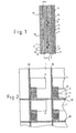
- FIG. 1 is a sectional view of a part of a multi-color flat display, which is a preferred embodiment of the invention, wherein, behind a glass substrate 1 on one side, there are formed a transparent electrode 2, an electroluminescent layer 3 consisting of ZnS doped with TbF 3 emitting green electroluminescent light, another electroluminescent layer 4 comprising ZnS doped with SmF 3 emitting red electroluminescent light and another electrode 5 having a light-reflective face.
- switching elements each built into one or another pixel, of thin-film transistor (TFT) structure of amorphous Si.
- TFT thin-film transistor
- Each TFT consists of an Mo gate electrode 6, an Si 3 N 4 insulating layer 7, an amorphous Si layer 8, an Mo source electrode 9 and an Mo drain electrode 10, and to the drain electrode 10 is connected an indium tin oxide (ITO) electrode 11.
- the TFT is covered with an Si 3 N 4 protective film 12.
- the gate electrode and source electrode of the TFT are composed of a part each of the gate signal electrode and of the source signal electrode, respectively, and driving electric signals from outside the panel are fed by the gate signal electrode and source signal electrode to the gate electrode and source electrode, respectively, to operate the TFT.
- FIG. 2 is a front view showing the matrix arrangement of the array of switching elements of TFT structure formed inside the glass substrate 1 and the signal electrodes in a part of the panel illustrated in FIG. 1.
- reference numerals 26 represent gate signal electrodes and 29, source signal electrodes, a part of each constituting a gate electrode 6 or a source electrode 9, whichever is pertinent.
- Numerals 8, 10 and 11 respectively refer to an amorphous Si, an Mo drain electrode and an ITO pixel electrode as in FIG. 1.
- color filters 14 passing green light and color filters 15 passing red light in such positions as correspond to pixel electrodes, and all over them is formed an ITO common electrode 16.
- the color filters 14 and 15 are prepared by dyeing polyether sulfone resin with a mixture of Sumicaron E-FBL and Sumicaron E-4GL and Eastman Scarlet BG, respectively.
- a polarizing film 17 To the outside of this glass substrate 13 is attached a polarizing film 17 for the purpose of improving the contrast of images.
- the multi-color flat display panel is fabricated by positioning opposite to each other the two glass substrates 1 and 13 of such structures with an approximately 10-micron gap in-between and filling the gap with a liquid crystal material prepared by adding a suitable quantity of chiral nematic liquid crystals CM15 (a product of Chisso Corp.) to mixed liquid crystals ZLI1841 (a product of E. Merck) containing black dichroic dyes.
- CM15 a product of Chisso Corp.
- ZLI1841 a product of E. Merck
- FIG. 3 illustrating the positional relationship between the split structure of color filters and pixels in the embodiment of FIG. 1, is a front view seen from the a-b position in FIG. 1.
- reference numerals 11 represent the same ITO pixel electrodes as in FIG. l, each of which constitutes a display pixel.
- 14 and 15 refer to the same color filters as in FIG. 1, respectively passing green and red lights, and they are so positioned as to be in one-to-one correspondence with the display pixels 11.
- a TFT-structured switching element connected from a gate electrode 6 to the corresponding gate signal electrode 26 is kept “on” as long as the pulse voltage is applied, and the voltage of about 10 V impressed on a source signal electrode 29 causes the electric charge to shift from a source electrode 9, connected to the corresponding source signal electrode 29, by way of a drain electrode 10 to an ITO pixel electrode 11.
- the source signal electrode is maintained at 0 V, even though the switching element is "on", no electric field will be generated between the pixel electrode pertinent to that source signal electrode and the common electrode.
- the liquid crystal molecules are uniformly oriented in parallel with the electrode faces.
- the absorption of light rays of all wavelengths by the black dichroic dyes causes the liquid crystal layer to pass virtually no light. This effect is reinforced by the utilization of linearly polarized light in only one direction by the use of the polarizing film 17.
- the multi-color flat display panel according to the present invention uses color filters.
- the color filters 14 and 15 have the transmission spectra shown in FIGS. 5a and 5b, respectively.
- the color filter 14 effectively passes the main wavelength of the green luminescent light emitted from the electroluminescent layer 3
- a pixel provided with a color filter 14 if a pixel provided with a color filter 14 is selected, there is transmitted vivid green light having a very steep spectrum.
- the color filter 15 effectively passes the main wavelength of the red luminescent light emitted from the electroluminescent layer 4
- a pixel provided with a color filter 15 if a pixel provided with a color filter 15 is selected, there is transmitted vivid red light having a very steep spectrum. Even the light passed by a color filter cannot give a completely separated spectrum, like the one shown in FIG.
- the multi-color flat display panel according to the present invention in which color filters are so structured as to spectrally validly and effectively select lights emitted from electroluminescent layers, can give very vivid color images even if the illumination light emitted from the electroluminescent layers is not perfectly colorless. Moreover, obviously, the display can be built far thinner than one having a fluorescent lamp as light source for the illuminating purpose.
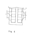
- FIG. 6 is a front view of another color filter structure that can be used in the present invention, further illustrating the positional relationship between the color filters and display pixels.
- each of the reference numerals 11 represents, as in FIG. 1, an ITO pixel electrode, which constitutes one display pixel.
- display pixels on the left hand side make up one group, Group A, and ones on the right hand side form another, Group B.
- 14 and 15 respectively refer to a color filter passing green light and another passing red light, like in FIG. 1, and the color filters 14 and 15 are so positioned as to respectively correspond to Groups A and B of display pixels on a one-to-one basis.
- This embodiment especially if it is a very fine display panel having a large display capacity, does not require the arrangement of color filters in a finely dotted pattern, permits a high production yield and accordingly costs less. Of course, like the first preferred embodiment, it is capable of vivid color representation.
- the color filters 14 and 15 are formed on the glass substrate 13 in the foregoing embodiments as shown in.FIG. 1, they may as well be formed overlapped on the ITO pixel electrodes 11 on the other glass substrate 1.
- the present invention is applicable to any operational mode in which light transmission and light interception can be effectively switched between each other according to the selection or non-selection of display pixel, such as a twist nematic mode.
- the switching elements for connecting each display pixels to liquid crystal layers are not restricted to thin-film transistors of amorphus Si which are used in this embodiment.
- the present invention can provide a flat display panel capable of vivid multi-color representation and having a large display capacity.
Landscapes
- Physics & Mathematics (AREA)
- Nonlinear Science (AREA)
- Mathematical Physics (AREA)
- Chemical & Material Sciences (AREA)
- Crystallography & Structural Chemistry (AREA)
- General Physics & Mathematics (AREA)
- Optics & Photonics (AREA)
- Engineering & Computer Science (AREA)
- Microelectronics & Electronic Packaging (AREA)
- Devices For Indicating Variable Information By Combining Individual Elements (AREA)
Abstract
Description
- The present invention relates to a flat display panel capable of vivid representation in multiple colors and having a large display capacity.
- There is a great demand for graphic and/or character display units, especially for use in office automation systems and various computer systems, and there further are pressing requirements on these display units for multi-color representation capability and large display capacities. To meet these requirements, cathode ray tubes (CRTs) are commonly used. However, CRTs have such disadvantages as large cubic measures, heavy weights and screen flickers, which invite eye strain on the part of their users, and accordingly there is an urgent call for the development of a new type flat display panel, free of these disadvantages.
- To meet this call have been developed the plasma display panel (PDP), electroluminescent (EL) panel and liquid crystal display (LCD) panel, which, however, are still inadequate in performance, especially unsatisfactory in multi-color representation capability. Among these new types of flat display panel, what is considered the most likely to replace the CRT display is the LCD panel.
- Expansion of the LCD's representation capacity is realized by laying a switching element over each display picture element (pixel). Switching elements used for this purpose include thin-film transistors (TFTs) of polycrystalline Si, monocrystalline Si, amorphous Si or Te. The methods of color representation include multi- coloring of the background plate or providing each pixel with a color filter. Thus, the liquid crystal (LC) layer functions as a light shutter in the twist nematic (TN) mode or black guest-host (GH) mode, so that the color of the background plate or of the color filter is seen at the pixel where the liquid crystal layer is on, or the pixel where it is off appears black. An example of this kind of LCD is reported on by S. Morozumi et al in their article entitled "B/W and Color LC Video Displays Addressed by Poly Si TFTs" in SID 83 Digest (1983), pp. 156-157.
- However, this type LCD, if used in a reflective mode, is insufficient in brightness and accordingly unpractical, and has to be used in a transmissive mode. Whereas the LCD reported on by Morozumi and his associates is a transmissive version, they state nothing as to the type of back lighting. A fluorescent lamp is conventionally used for back lighting in an LCD, but this kind of lamp, even a flat one, is rather thick, and therefore ruins the important feature of the LCD as a thin display. Moreover, in a display of a relatively large area, the fluorescent lamp has the additional disadvantage of being unable to always ensure uniform illumination.
- There has been an attempt to use an electroluminescent (EL) light source, instead of the fluorescent lamp which has these disadvantages, in a monochrome LCD (Nikkei Electronics, Jan. 31, 1983, p. 67). However, no conventional method permitted the use of an EL light source for the illumination of a color LCD, because light from the EL, unlike that from the fluorescent lamp, cannot be made colorless. Even what is the closest to colorless light among the currently available, for instance that mentioned in the above-cited reference, is slightly yellow, and no such EL light source can give any shade of blue. Thus, the LCD, which is considered the foremost among the known alternatives to meet the demand for a flat color display having a large capacity, is still unsatisfactory, especially in terms of color representation capability.
- An object of the present invention, therefore, is to provide a flat display panel capable of vivid multi- color representation and having a large display capacity.
- The multi-color flat display panel according to the invention is characterized in that it is provided with electroluminescent layers for illuminating the whole display screen from behind; color filters of a plurality of colors for selectively transmitting in a spectral manner the lights emitted by the electroluminescent layers; liquid crystal layers for selectively transmitting or intercepting electroluminescent lights entering from or passing to the color filters; and switching elements connected to the liquid crystal layers on a pixel-by-pixel basis.
-
- FIG. 1 is a sectional view of a part of a liquid crystal panel, which is a preferred embodiment of the present invention;
- FIG. 2 is a front view showing the arrangement of switching elements formed over the
substrate 1 relating to the embodiment of the invention: - FIG. 3 is a front view of the a-b section of FIG. 1 and shows the arrangement of filters and pixel electrodes;
- FIGS. 4a and 4b are graphs showing the emission spectra of the electroluminescent layer 3 and the electroluminescent layer 4, respectively, relating to the embodiment of the invention;
- ' FIGS. 5a and 5b are graphs showing the transmission characteristics of the
filters - FIG. 6 is a front view showing an alternative arrangement of filters and pixel electrodes, which can be used in the embodiment of the invention.
- Other features and advantages of the present invention will be more apparent from the detailed description hereunder taken in conjunction with the accompanying drawings. FIG. 1 is a sectional view of a part of a multi-color flat display, which is a preferred embodiment of the invention, wherein, behind a
glass substrate 1 on one side, there are formed atransparent electrode 2, an electroluminescent layer 3 consisting of ZnS doped with TbF3 emitting green electroluminescent light, another electroluminescent layer 4 comprising ZnS doped with SmF3 emitting red electroluminescent light and anotherelectrode 5 having a light-reflective face. Inside theglass substrate 1 are switching elements, each built into one or another pixel, of thin-film transistor (TFT) structure of amorphous Si. Each TFT consists of anMo gate electrode 6, an Si3N4insulating layer 7, anamorphous Si layer 8, anMo source electrode 9 and anMo drain electrode 10, and to thedrain electrode 10 is connected an indium tin oxide (ITO)electrode 11. The TFT is covered with an Si3N4protective film 12. The gate electrode and source electrode of the TFT are composed of a part each of the gate signal electrode and of the source signal electrode, respectively, and driving electric signals from outside the panel are fed by the gate signal electrode and source signal electrode to the gate electrode and source electrode, respectively, to operate the TFT. - Next will be described how these electrodes are formed with reference to FIG. 2, which is a front view showing the matrix arrangement of the array of switching elements of TFT structure formed inside the
glass substrate 1 and the signal electrodes in a part of the panel illustrated in FIG. 1. In FIG. 2,reference numerals 26 represent gate signal electrodes and 29, source signal electrodes, a part of each constituting agate electrode 6 or asource electrode 9, whichever is pertinent.Numerals - Referring again to FIG. 1, inside the
other glass substrate 13 are alternately formedcolor filters 14 passing green light andcolor filters 15 passing red light in such positions as correspond to pixel electrodes, and all over them is formed an ITOcommon electrode 16. Thecolor filters glass substrate 13 is attached a polarizingfilm 17 for the purpose of improving the contrast of images. The multi-color flat display panel is fabricated by positioning opposite to each other the twoglass substrates - FIG. 3, illustrating the positional relationship between the split structure of color filters and pixels in the embodiment of FIG. 1, is a front view seen from the a-b position in FIG. 1. In FIG. 3,
reference numerals 11 represent the same ITO pixel electrodes as in FIG. l, each of which constitutes a display pixel. Further in FIG. 3, 14 and 15 refer to the same color filters as in FIG. 1, respectively passing green and red lights, and they are so positioned as to be in one-to-one correspondence with thedisplay pixels 11. - In a panel of this structure, as D.C. voltage pulses of around 15 V are successively applied to a
gate signal electrode 26, a TFT-structured switching element connected from agate electrode 6 to the correspondinggate signal electrode 26 is kept "on" as long as the pulse voltage is applied, and the voltage of about 10 V impressed on asource signal electrode 29 causes the electric charge to shift from asource electrode 9, connected to the correspondingsource signal electrode 29, by way of adrain electrode 10 to anITO pixel electrode 11. Therefore, if the electric potentials of apixel electrode 11 and the corresponding ITOcommon electrode 16 are set at the ground level (0 V), an electric field will be generated in the part of the liquid crystal layer sandwiched between the twoelectrodes - On the other hand, if the source signal electrode is maintained at 0 V, even though the switching element is "on", no electric field will be generated between the pixel electrode pertinent to that source signal electrode and the common electrode. In the parts of the liquid crystal layer which are either over the pixel electrode of such a pixel (unselected pixel) or facing no pixel electrode, the liquid crystal molecules are uniformly oriented in parallel with the electrode faces. As a result, in these regions, or elsewhere than the region of the selected pixel electrode, the absorption of light rays of all wavelengths by the black dichroic dyes causes the liquid crystal layer to pass virtually no light. This effect is reinforced by the utilization of linearly polarized light in only one direction by the use of the polarizing
film 17. - Since gate signal electrodes are successively scanned, when the pulse voltage applied on the gate electrode is eliminated, the switching element is turned off, so that the voltage applied to the source signal electrode is not conveyed to the drain electrode and the shift of electric charge to the ITO pixel electrode is discontinued. However, because the electric charge, once stored in the selected pixel, is maintained for a duration determined by a CR time constant, the forced orientation of the liquid crystal molecules by the electric field, and consequently the transparent state of the pixel, will be retained until the scanning of gate signal electrodes recurs if the time constant value is sufficiently great. This is the effect of the TFT-structured switching elements, which makes even time-division driving in a line-at-a-time addressing scheme, as viewed from liquid crystals, similar to static driving, and accordingly permits ready realization of a large-capacity display where many electrodes have to be scanned.
- To describe the functioning of the electroluminescent layers, supplying an A.C. voltage between the
transparent electrode 2 and theelectrode 5 having a light-reflective face causes the first such layer 3 to emit green luminescent light having the spectrum of FIG. 4a and the second such layer 4 to emit red luminescent light having the spectrum of FIG. 4b. Therefore, these luminescent lights alone constitute a sum of the spectra of FIGS. 4a and 4b. (As regards a double-layer structured electroluminescence panel, there is known, for instance a report by R.E. Coovert et al., entitled "Feasibility of a Dual-Color ACTFEL Display" and published in SID 82 Digest, pp. 128-129.) This light of the synthesized spectrum, as seen from the spectra of FIGS. 4a and 4b, is far from being colorless and, as it is, can give no satisfactory color display, as described with reference to prior art. - The multi-color flat display panel according to the present invention uses color filters. The color filters 14 and 15 have the transmission spectra shown in FIGS. 5a and 5b, respectively. Thus, as the
color filter 14 effectively passes the main wavelength of the green luminescent light emitted from the electroluminescent layer 3, if a pixel provided with acolor filter 14 is selected, there is transmitted vivid green light having a very steep spectrum. Similarly, as thecolor filter 15 effectively passes the main wavelength of the red luminescent light emitted from the electroluminescent layer 4, if a pixel provided with acolor filter 15 is selected, there is transmitted vivid red light having a very steep spectrum. Even the light passed by a color filter cannot give a completely separated spectrum, like the one shown in FIG. 5a or 5b, but light of wavelengths in the vicinity of 590 nm or above 660 nm is transmitted, though only slightly, by both color filters. Therefore, if light of wavelengths in one or more of, these regions is emitted from the light source behind, separation by the color filters will become inadequate, resulting in deteriorated chroma of the display colors. In the light emitted from the electroluminescent layers of this embodiment, however, the components of wavelengths in these regions are negligibly small, and moreover the lights of 550 nm and 650 nm, the main wavelengths of the lights emitted from the electroluminescent layers, effectively pass the respectively corresponding color filters. - . It is thus seen that the multi-color flat display panel according to the present invention, in which color filters are so structured as to spectrally validly and effectively select lights emitted from electroluminescent layers, can give very vivid color images even if the illumination light emitted from the electroluminescent layers is not perfectly colorless. Moreover, obviously, the display can be built far thinner than one having a fluorescent lamp as light source for the illuminating purpose.
- FIG. 6 is a front view of another color filter structure that can be used in the present invention, further illustrating the positional relationship between the color filters and display pixels. In FIG. 6, each of the
reference numerals 11 represents, as in FIG. 1, an ITO pixel electrode, which constitutes one display pixel. In FIG. 6, display pixels on the left hand side make up one group, Group A, and ones on the right hand side form another, Group B. Further in the figure, 14 and 15 respectively refer to a color filter passing green light and another passing red light, like in FIG. 1, and thecolor filters - To add, though the
color filters glass substrate 13 in the foregoing embodiments as shown in.FIG. 1, they may as well be formed overlapped on theITO pixel electrodes 11 on theother glass substrate 1. - Whereas the foregoing description, with a view to simplification, limits itself to embodiments having two electroluminescent layers, exactly the same effect can be realized with a single electroluminescent layer formed by mixing the two sets of electroluminescent materials to emit light having a spectrum combining the spectra of FIGS. 4a and 4b. Obviously, the display colors are not restricted to the ones used in these embodiments. Nor is their number limited to two.
- Although the foregoing description refers to embodiments in which liquid crystal layers operate in a guest-host mode, the present invention is applicable to any operational mode in which light transmission and light interception can be effectively switched between each other according to the selection or non-selection of display pixel, such as a twist nematic mode. Further, though perhaps reduncant to state in particular, the switching elements for connecting each display pixels to liquid crystal layers are not restricted to thin-film transistors of amorphus Si which are used in this embodiment.
- As hitherto described, the present invention can provide a flat display panel capable of vivid multi-color representation and having a large display capacity.
Claims (1)
- A multi-color flat display panel comprising:eletroluminiscent layers (3,4) for illuminating the whole display screen from behind;color filters (14, 15) of a plurality of colors for selectively transmitting in a spectral manner the lights emitted by said electroluminiscent layers;liquid crystal layers for selectively transmitting or intercepting electroluminiscent lights entering from or passing to said color filters (14, 15);transparent pixel electrodes (11) arranged at prescribed intervals in connection with said liquid crystal layers;
and switching elements (6 to 10) for applying electric fields on said transparent pixel electrodes (11), wherein said color filters (14, 15) are so positioned as to correspond to said transparent pixel electrodes or groups of said tranaparent pixel electrodes on a one-to-one basis and at least one of color filters adjoining each of said color filters has a different selective characteristic.
Applications Claiming Priority (4)
| Application Number | Priority Date | Filing Date | Title |
|---|---|---|---|
| JP111345/83 | 1983-06-21 | ||
| JP58111343A JPS602980A (en) | 1983-06-21 | 1983-06-21 | Multicolor flat display panel |
| JP111343/83 | 1983-06-21 | ||
| JP58111345A JPS602981A (en) | 1983-06-21 | 1983-06-21 | Multicolor flat display panel |
Publications (1)
| Publication Number | Publication Date |
|---|---|
| EP0129867A1 true EP0129867A1 (en) | 1985-01-02 |
Family
ID=26450761
Family Applications (1)
| Application Number | Title | Priority Date | Filing Date |
|---|---|---|---|
| EP19840107168 Withdrawn EP0129867A1 (en) | 1983-06-21 | 1984-06-22 | Multi-color flat display panel |
Country Status (1)
| Country | Link |
|---|---|
| EP (1) | EP0129867A1 (en) |
Cited By (3)
| Publication number | Priority date | Publication date | Assignee | Title |
|---|---|---|---|---|
| EP0267686A1 (en) * | 1986-10-23 | 1988-05-18 | Litton Systems Canada Limited | Full colour liquid crystal display |
| FR2643488A1 (en) * | 1989-02-21 | 1990-08-24 | France Etat | ELECTROLUMINESCENT POLYCHROME DISPLAY DISPLAY WITH MEMORY EFFECT |
| WO1993016410A1 (en) * | 1992-02-14 | 1993-08-19 | Raychem Corporation | Front lit liquid crystal displays |
Citations (3)
| Publication number | Priority date | Publication date | Assignee | Title |
|---|---|---|---|---|
| US3840695A (en) * | 1972-10-10 | 1974-10-08 | Westinghouse Electric Corp | Liquid crystal image display panel with integrated addressing circuitry |
| GB1509643A (en) * | 1975-05-02 | 1978-05-04 | Hughes Aircraft Co | Liquid crystal dot colour display |
| DE2722388B2 (en) * | 1976-05-13 | 1979-03-01 | Ebauches S.A., Neuenburg (Schweiz) | Passive electro-optical display arrangement |
-
1984
- 1984-06-22 EP EP19840107168 patent/EP0129867A1/en not_active Withdrawn
Patent Citations (3)
| Publication number | Priority date | Publication date | Assignee | Title |
|---|---|---|---|---|
| US3840695A (en) * | 1972-10-10 | 1974-10-08 | Westinghouse Electric Corp | Liquid crystal image display panel with integrated addressing circuitry |
| GB1509643A (en) * | 1975-05-02 | 1978-05-04 | Hughes Aircraft Co | Liquid crystal dot colour display |
| DE2722388B2 (en) * | 1976-05-13 | 1979-03-01 | Ebauches S.A., Neuenburg (Schweiz) | Passive electro-optical display arrangement |
Cited By (4)
| Publication number | Priority date | Publication date | Assignee | Title |
|---|---|---|---|---|
| EP0267686A1 (en) * | 1986-10-23 | 1988-05-18 | Litton Systems Canada Limited | Full colour liquid crystal display |
| FR2643488A1 (en) * | 1989-02-21 | 1990-08-24 | France Etat | ELECTROLUMINESCENT POLYCHROME DISPLAY DISPLAY WITH MEMORY EFFECT |
| EP0384829A1 (en) * | 1989-02-21 | 1990-08-29 | France Telecom | Multicolour electroluminescent flat panel display having a memory effect |
| WO1993016410A1 (en) * | 1992-02-14 | 1993-08-19 | Raychem Corporation | Front lit liquid crystal displays |
Similar Documents
| Publication | Publication Date | Title |
|---|---|---|
| EP0336351B1 (en) | Controlled color filter for use in information display applications | |
| US5337068A (en) | Field-sequential display system utilizing a backlit LCD pixel array and method for forming an image | |
| US6570554B1 (en) | Liquid crystal display | |
| JP2582644B2 (en) | Flat panel image display | |
| US7755597B2 (en) | Liquid crystal display device and driving method used in same | |
| US4924215A (en) | Flat panel color display comprising backlight assembly and ferroelectric liquid crystal shutter assembly | |
| US20020145685A1 (en) | Blue backlight and phosphor layer for a color LCD | |
| US7639324B2 (en) | Liquid crystal display device | |
| US20060125982A1 (en) | Liquid crystal display | |
| US6184951B1 (en) | Liquid crystal display wherein each pixels of first layer is optically aligned with respective group of pixels of second layer | |
| US7006171B1 (en) | Light-control device and method of driving | |
| US6600467B1 (en) | Flat panel display architecture | |
| US20080084521A1 (en) | Field sequentially driven liquid crystal display device | |
| US20050046765A1 (en) | Dual-sided flat panel display structure and operating method thereof | |
| JP2000028984A (en) | Display control method for liquid crystal display device and liquid crystal display device | |
| US7697089B2 (en) | Liquid crystal display apparatus | |
| JPS61121033A (en) | Liquid crystal color display device | |
| Uchida | Multicolored liquid crystal displays | |
| EP0129867A1 (en) | Multi-color flat display panel | |
| JP2004333583A (en) | Liquid crystal display device | |
| JPH08166589A (en) | Liquid crystal display element | |
| JPH0554642B2 (en) | ||
| JPS61231586A (en) | Color liquid crystal display unit | |
| KR20000022608A (en) | Display device | |
| US20040041783A1 (en) | Reflective liquid crystal display and driving method thereof |
Legal Events
| Date | Code | Title | Description |
|---|---|---|---|
| PUAI | Public reference made under article 153(3) epc to a published international application that has entered the european phase |
Free format text: ORIGINAL CODE: 0009012 |
|
| 17P | Request for examination filed |
Effective date: 19840622 |
|
| AK | Designated contracting states |
Designated state(s): DE FR GB |
|
| 17Q | First examination report despatched |
Effective date: 19860903 |
|
| STAA | Information on the status of an ep patent application or granted ep patent |
Free format text: STATUS: THE APPLICATION IS DEEMED TO BE WITHDRAWN |
|
| 18D | Application deemed to be withdrawn |
Effective date: 19870314 |
|
| RIN1 | Information on inventor provided before grant (corrected) |
Inventor name: TANAKA, TAKANORI Inventor name: NAEMURA, SHOHEI Inventor name: SAKUMA, HIRAKU Inventor name: TANI, CHIZUKA Inventor name: SAITO, TAKESHI Inventor name: NUNOMURA, KEIJI |