EP0129707B1 - Magnetically sensitive semiconductor devices - Google Patents
Magnetically sensitive semiconductor devices Download PDFInfo
- Publication number
- EP0129707B1 EP0129707B1 EP84105752A EP84105752A EP0129707B1 EP 0129707 B1 EP0129707 B1 EP 0129707B1 EP 84105752 A EP84105752 A EP 84105752A EP 84105752 A EP84105752 A EP 84105752A EP 0129707 B1 EP0129707 B1 EP 0129707B1
- Authority
- EP
- European Patent Office
- Prior art keywords
- emitter
- schottky barrier
- junction
- substrate
- magnetically sensitive
- Prior art date
- Legal status (The legal status is an assumption and is not a legal conclusion. Google has not performed a legal analysis and makes no representation as to the accuracy of the status listed.)
- Expired
Links
- 239000004065 semiconductor Substances 0.000 title claims description 7
- 230000004888 barrier function Effects 0.000 claims description 45
- 239000000758 substrate Substances 0.000 claims description 35
- 238000002347 injection Methods 0.000 claims description 30
- 239000007924 injection Substances 0.000 claims description 30
- 239000000969 carrier Substances 0.000 claims description 21
- 229910052751 metal Inorganic materials 0.000 claims description 14
- 239000002184 metal Substances 0.000 claims description 14
- XUIMIQQOPSSXEZ-UHFFFAOYSA-N Silicon Chemical compound [Si] XUIMIQQOPSSXEZ-UHFFFAOYSA-N 0.000 claims description 11
- 229910052710 silicon Inorganic materials 0.000 claims description 11
- 239000010703 silicon Substances 0.000 claims description 11
- VBJZVLUMGGDVMO-UHFFFAOYSA-N hafnium atom Chemical compound [Hf] VBJZVLUMGGDVMO-UHFFFAOYSA-N 0.000 claims description 9
- 229910052735 hafnium Inorganic materials 0.000 claims description 6
- HCHKCACWOHOZIP-UHFFFAOYSA-N Zinc Chemical compound [Zn] HCHKCACWOHOZIP-UHFFFAOYSA-N 0.000 claims description 5
- QCWXUUIWCKQGHC-UHFFFAOYSA-N Zirconium Chemical compound [Zr] QCWXUUIWCKQGHC-UHFFFAOYSA-N 0.000 claims description 5
- 229910052726 zirconium Inorganic materials 0.000 claims description 5
- 230000004044 response Effects 0.000 claims description 4
- 229910052725 zinc Inorganic materials 0.000 claims description 4
- 239000011701 zinc Substances 0.000 claims description 4
- XAGFODPZIPBFFR-UHFFFAOYSA-N aluminium Chemical compound [Al] XAGFODPZIPBFFR-UHFFFAOYSA-N 0.000 description 11
- 229910052782 aluminium Inorganic materials 0.000 description 10
- 239000013598 vector Substances 0.000 description 10
- 239000000463 material Substances 0.000 description 9
- 230000004907 flux Effects 0.000 description 8
- 238000009792 diffusion process Methods 0.000 description 6
- 230000000694 effects Effects 0.000 description 6
- 230000035945 sensitivity Effects 0.000 description 6
- 238000010438 heat treatment Methods 0.000 description 5
- 238000002513 implantation Methods 0.000 description 5
- 229910021332 silicide Inorganic materials 0.000 description 5
- FVBUAEGBCNSCDD-UHFFFAOYSA-N silicide(4-) Chemical compound [Si-4] FVBUAEGBCNSCDD-UHFFFAOYSA-N 0.000 description 4
- VYPSYNLAJGMNEJ-UHFFFAOYSA-N Silicium dioxide Chemical compound O=[Si]=O VYPSYNLAJGMNEJ-UHFFFAOYSA-N 0.000 description 2
- TWRSDLOICOIGRH-UHFFFAOYSA-N [Si].[Si].[Hf] Chemical compound [Si].[Si].[Hf] TWRSDLOICOIGRH-UHFFFAOYSA-N 0.000 description 2
- 239000011248 coating agent Substances 0.000 description 2
- 238000000576 coating method Methods 0.000 description 2
- 238000005516 engineering process Methods 0.000 description 2
- 238000005530 etching Methods 0.000 description 2
- 150000002739 metals Chemical class 0.000 description 2
- 238000000034 method Methods 0.000 description 2
- 230000026683 transduction Effects 0.000 description 2
- 238000010361 transduction Methods 0.000 description 2
- 230000002411 adverse Effects 0.000 description 1
- 229910052785 arsenic Inorganic materials 0.000 description 1
- RQNWIZPPADIBDY-UHFFFAOYSA-N arsenic atom Chemical compound [As] RQNWIZPPADIBDY-UHFFFAOYSA-N 0.000 description 1
- 230000008901 benefit Effects 0.000 description 1
- 238000000151 deposition Methods 0.000 description 1
- 230000008021 deposition Effects 0.000 description 1
- 238000000227 grinding Methods 0.000 description 1
- BHEPBYXIRTUNPN-UHFFFAOYSA-N hydridophosphorus(.) (triplet) Chemical compound [PH] BHEPBYXIRTUNPN-UHFFFAOYSA-N 0.000 description 1
- 239000012212 insulator Substances 0.000 description 1
- 230000003993 interaction Effects 0.000 description 1
- 238000004519 manufacturing process Methods 0.000 description 1
- 238000001465 metallisation Methods 0.000 description 1
- 230000008569 process Effects 0.000 description 1
- 238000005215 recombination Methods 0.000 description 1
- 230000006798 recombination Effects 0.000 description 1
- 230000009467 reduction Effects 0.000 description 1
- 235000012239 silicon dioxide Nutrition 0.000 description 1
- 239000000377 silicon dioxide Substances 0.000 description 1
- 239000007787 solid Substances 0.000 description 1
- 238000003860 storage Methods 0.000 description 1
Images

Classifications
-
- H—ELECTRICITY
- H10—SEMICONDUCTOR DEVICES; ELECTRIC SOLID-STATE DEVICES NOT OTHERWISE PROVIDED FOR
- H10D—INORGANIC ELECTRIC SEMICONDUCTOR DEVICES
- H10D48/00—Individual devices not covered by groups H10D1/00 - H10D44/00
- H10D48/40—Devices controlled by magnetic fields
Definitions
- This invention relates to magnetically sensitive semiconductive devices, and more particularly to new magnetically sensitive semiconductive devices having Schottky barrier junctions.
- the invention as claimed is intended to provide an improved magnetically sensitive semiconductor device having uniplanar minority carrier Schottky injection at an emitter or cathode.
- the invention is also intended to provide an improved semiconductive magnetically sensitive device having high frequency operating characteristics.
- the Schottky barrier is preferably constructed using hafnium, zirconium, zinc, or any similar material that can form a silicide layer at the surface of P-type silicon substrates and having a work function potential cp " less than 4,8 volts. Because no unwanted perimeter injection exists from the Schottky barrier, i.e., it is a uniplanar, unidirectional injection source, it is not necessary to remove the collectors or anodes to a distance more widely separated from the source of minority carriers in order to emphasize the contribution of those carriers injected in the desired direction.
- the carriers may all be injected in the desired vertical direction for maximum sensitivity to magnetic flux directed parallel to the surface of the substrate, the collectors or anodes can be brought very close to the emissive surface. This, in turn, leads to a high frequency capability due to the short carrier transit times.
- Both vertical and lateral diode and transistor structures are possible and have been constructed as shown herein.
- the metals hafnium, zirconium, and zinc form appropriate silicides with silicon substrates when a heat treatment is carried out.
- the heat treatment is generally known in the art and will not be described in detail herein. Briefly, it consists in heating the substrate on whose surface has been deposited the appropriate metal in the desired areas to a temperature approximating 538°C until a metallic silicide is formed at the junction between the two materials.
- the barrier potential (())s ⁇ Pm) for hafnium silicide that provides a reliable Schottky barrier is approximately a negative 0,95 volts at room temperature.
- Zirconium and zinc also have a suitable Schottky barrier potential of approximately negative 0.8 volts and negative 0.53 volts, respectively, at room temperature.
- the other elements also form suitable barriers but are less desirable insofar as they are presently understood.
- Base or anode ohmic output contacts can be made using ordinary aluminum for example, but Schottky barrier contacts of the desired metal can also be used. It is only necessary that a good ohmic base contact or anode contact be made. This can be achieved by heavily doping a P-region in the substrate in the area in which the aluminum is to make ohmic contacts for the collector or anode outputs.
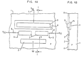
- FIG. 1A a form of a Schottky barrier magnetically sensitive transistor is illustrated in Figures 1A and 1B.
- Figure 1A a plan view with the overlying oxide coating of the semiconductive substrate removed for clarity is shown.
- Semiconductive substrate 1 is supplied with a metallic rectifying emitter contact 2.
- hafnium metal is used and a heat treatment as mentioned above is performed to create a hafnium silicide layer at the junction between the substrate 1 and the emitter metal 2.
- Two hafnium metal collectors with similar silicide barrier layers are deposited as collectors 3. The collectors are spaced on either side of an imaginary plan constructed perpendicular to the emissive surface and passing through the Lorentz potential null line of the emitter area.
- the hafnium emitter junction is forward biased by applying a positive voltage V BB to the base contact 9 while grounding the emitter contact 2.
- Base contact 9 can be ordinary aluminum making only ohmic contact with the surface of the semiconductive substrate 1.
- P-type substrates make good ohmic contact with aluminum and, to achieve even better contact, a heavy doping P+ material in the vicinity of the base contact may be carried out. This is illustrated as the implanted area 4 with the actual aluminum contact shown as 9 in Figures 1A and 1 B.
- a quiescent current will be caused to flow in the collector circuit comprising the load resistors 6 to which voltage V cc is applied. This can be sensed at the output terminals 5.
- This current can be controlled by the base voltage applied to the base at terminal 7 in a known manner.
- the quiescent current of the reverse biased collector is essentially balanced at the outset, but may be imbalanced by applying a magentic field vector parallel to the surface of the emitter.
- the emitter injects all minority carriers in the same direction, in this case, directly into the substrate in a vertical manner.
- these carriers will intercept the magnetic flux vector at right angles and produce the maximum Lorentz potential along the bottom single plane of the emitter junction.
- the application of a magnetic field parallel to this plane modulates the forward bias voltage occurring at the emitter junction since the Lorentz potential is greater at one side of the emitter than at the other and increases injection toward the one side while suppressing it toward the other.
- a null line exists between the two extremes of the Lorentz voltage.
- the effect is such that the left half Schottky emitter junction will inject more electrons than the right half.
- electrons are the minority carriers as required for operation.
- the emitted minority carriers stream toward the two spaced apart collectors 3 and are drawn off through the load resistors 6. This results in a differential collector current which can be sensed as a differential voltage between the output terminals 5. This occurs as a result of the left collector receiving an increase in minority carrier flow while the right collector experiences a decrease in minority carrier flow. The total emitter current remains unchanged.
- Perimeter injection is undesirable since this leads to a reduction in sensitivity for the desired magnetic field components and will account for a magnetic sensitivity to field components directed other than in the desired direction. If fields other than that preferred are employed, sensitivity to flux in unwanted directions cannot be distinguished at the output from that which is desired.
- the sensor height and length will be typically 1.0 and 4.0 micrometers, respectively.
- the mounted and packaged sensor must also be brought close to the magnetically recorded medium. Consequently, a grinding and lapping process will ordinarily be carried out that may come close to an edge of the emitter part and actually lap away a portion of it.
- the Schottky junction is essentially unaffected by a removal of a small portion along its edge.
- Magnetically sensitive Schottky diodes and transistors depend on minority carrier injection.
- the injected minority carriers reduce conductivity in the region between the emitter or cathode and the output base, collector or anodes.
- a high level injection of minority carriers with base resistivities in excess of 2 ohm centimeters can satisfy the desired criteria.
- Figure 3 illustrates a magnetically sensitive Schottky barrier diode formed using hafnium, zirconium or zinc metal contacts as the cathode 2 in contact with a P-type silicon substrate 1.
- the magnetic field is, as in the previous Figure 1, oriented parallel to the surface of the junction such that modulation of injection across the junction will take place when the magnetic field is present.
- the preferential injection of minority carriers from the emissive surface of the cathode (or emitter) 2 will result in modulation of the anode (or base) conductivity that will lead to a differential output voltage measured at the output terminals 5 connected to the anode contacts 9 which through load resistors 6 are connected to the V EB voltage present at terminal 7.
- a heavy doped P+ material 4 may be present in the vicinity of the anode contact.
- FIG 2 a different magnetically sensitive lateral Schottky barrier transistor configuration is shown in plan view.
- the collectors 3 are relatively C-shaped and surround the ends of the metal emitter 2. However, the collectors 3 still reside on opposite sides of an imaginary plane passing through the Lorentz voltage null and perpendicular to the emissive surface as required for proper operation.
- the other elements are similarly numbered for the same purpose and function as that described with reference to Figures 1A and 1B.
- Placing the ohmic base contacts 9 at a symmetrically spaced distance relative to the emitter and the collectors results in attracting the minority carriers toward the direction of each collector to maximize collection of injected carriers. This enhances the overall sensitivity of the device.
- a signal output will be measured between the collector Schottky barriers 3 which also employ hafnium metal in the preferred embodiment as shown.
- the magnetic field vector B is shown in Figure 2 as parallel to the bottom surface of the emitter so that the maximum Lorentz potential modulation of the emitter injection will occur as described in my aforementioned references.
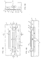
- FIGs 4A-4C a vertical Schottky barrier injection magnetically sensitive transistor is shown.
- FIG 4A a plan view of the elements in their arrangement on a semiconductive substrate 1 is shown.
- the Schottky emitter 2 is positioned on a top surface and directly above the two spaced apart collectors 3.
- Collector contacts 12 contact N+ doped regions which are diffused deeply to make contact with the N+ doped collectors located beneath the emitter; output terminals (not shown) like terminals 5 in Figure 1 are connected to collector contacts 12.
- the metallic base contact 9 makes contact with P+ doped base regions 4 since aluminum makes good ohmic contact with P+ material. N+ material also allows for good ohmic contact but this material is avoided here to prevent the creation of rectifying contacts at these points.
- FIG 4B shows a horizontal sectional elevation view along line AA in Figure 4A. It will be observed that the Schottky emitter 2 is provided with an aluminum top ohmic contact 10. The oxide layer 8 is shown in Figure 4B with windows opened up for the aluminum contact 12 and the Schottky emitter 2.
- This structure is built in a somewhat different fashion.
- a semiconductor substrate 1 which may be either P or intrinsic material for these purposes and is not an active part of the structure, is implanted with the collector regions 3. These are heavily N+ doped with arsenic, for example. These regions lie in the top region of the semiconductive substrate 1.
- an epitaxial layer 11 of a P- semiconductor material is laid down over the entire semiconductive substrate 1 and the collectors 3.
- a heavy doping of phosphorous for example which can be implanted or diffused to relatively great depths, is provided in region 13 to make contact with the N+ doped collectors from the top surface of the P- epitaxial layer.
- the oxide layer 8 will be grown or deposited and then an etching step is carried out to open up the contact windows for the aluminum contacts 12 for the collectors, for the base contacts 9, and in the region for the Schottky barrier emitter 2. The metal depositions for the Schottky barrier and for the contacts are then made.
- Figure 4C illustrates another sectional view BB through an end elevation of the structure shown in Figure 4A. It may be observed that the collectors 3 are directly beneath the emitter Schottky barrier 2 and are separated by the relatively thin P- layer 11. This means that the emissive surface of the Schottky barrier 2 is directly aligned with the collector surfaces 3. Lorentz modulation of emitter injection occurs at the Schottky barrier and will supply current more heavily to one collector 3 than the other depending on the direction of a magnetic flux vector. The most sensitive direction for interaction is when the magnetic flux vector passes parallel to the substrate and the emissive surface so as to be perpendicular to the direction of travel of the injected minority carriers.
- the Schottky barrier technology also provides an opportunity for creating magnetically sensitive diodes and transistors without diffusions or implantations into the substrate.
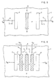
- Figure 5 illustrates a plan view of a Schottky barrier diode that is magnetically sensitive.
- the substrate 1 and the emitter or cathode 2 are constructed as explained above.
- the cathode 2 is a rectifying contact Schottky barrier junction.
- the base or anode contacts are ohmic contacts 9, which have output terminals 5 and are connected through load resistors 6 to voltage source V BB at terminals 7. It may be observed that the base and emitter are all in the same plane, do not require diffusions or implantations and are easily constructed.
- the magnetic vector B is also shown in Figure 5. It is directed parallel with the substrate 1 and the emissive surface of the cathode 2.
- the Lorentz potential will be developed at right angles to the magnetic vector and, in the case illustrated in Figure 5, along the shorter axis of the emitter 2.
- the null of the Lorentz potential will be on the center line or longitudinal axis of emitter 2 and it may be seen that the imaginary plane constructed perpendicular to the emissive surface and passing through the null of the Lorentz potential will also lie along this axis.
- the base or anode contacts in the case of a diode and collector contacts and base contacts in the case of a transistor will be located as described above on opposite sides of this imaginary plane.
- the base or anode contacts uniplanar and coplanar with the emitter, several important attributes result.
- Figure 6 illustrates in schematic plan view a magnetically sensitive transistor having in substrate 1 a Schottky barrier emitter 2, two ohmic base contacts 9 connected to voltage source V BB , and two spaced apart rectifying collectors 3 which have output terminals 5 and are connected through load resistors 6 to voltage source Vc c at terminals 7. It will be observed that the structure is similar to that in Figure 5 with the exception that rectifying collectors have been added between the base contacts and the emitter. The placement of the collector between the bases and the emitter and in the same plane as the emitter is important for the reasons noted with respect to the diode but also is easily constructed for the same reasons as well.
- the collectors 3 in Figure 6 are preferably the rectifying Schottky barrier contacts similar to the emitter 2. However, doped diffusions or implantations can also be utilized in a hybrid form of this transistor. It will be observed that in Figure 6 and Figure 5 as well, the base or anode contacts and the collector contacts as well, when present, are located on opposite sides of said imaginary plane and parallel therewith with the collectors spaced closer to the emitter than are the base contacts. This placement of the elements relative to one another enhances the effect of the Lorentz modulation of emitter injection by encouraging the minority carrier flow to occur directly between the emitter and the collectors or anodes. This means that virtually all carriers which are emitted will take part in and add to the eventual differential output signal, which equates to a high overall transduction efficiency.
Landscapes
- Electrodes Of Semiconductors (AREA)
- Hall/Mr Elements (AREA)
Applications Claiming Priority (2)
| Application Number | Priority Date | Filing Date | Title |
|---|---|---|---|
| US49910183A | 1983-05-27 | 1983-05-27 | |
| US499101 | 1983-05-27 |
Publications (2)
| Publication Number | Publication Date |
|---|---|
| EP0129707A1 EP0129707A1 (en) | 1985-01-02 |
| EP0129707B1 true EP0129707B1 (en) | 1988-02-24 |
Family
ID=23983821
Family Applications (1)
| Application Number | Title | Priority Date | Filing Date |
|---|---|---|---|
| EP84105752A Expired EP0129707B1 (en) | 1983-05-27 | 1984-05-21 | Magnetically sensitive semiconductor devices |
Country Status (4)
| Country | Link |
|---|---|
| EP (1) | EP0129707B1 (OSRAM) |
| JP (1) | JPS59222968A (OSRAM) |
| DE (1) | DE3469470D1 (OSRAM) |
| ES (1) | ES8503454A1 (OSRAM) |
Families Citing this family (1)
| Publication number | Priority date | Publication date | Assignee | Title |
|---|---|---|---|---|
| US5591996A (en) * | 1995-03-24 | 1997-01-07 | Analog Devices, Inc. | Recirculating charge transfer magnetic field sensor |
Family Cites Families (1)
| Publication number | Priority date | Publication date | Assignee | Title |
|---|---|---|---|---|
| US3167663A (en) * | 1962-08-06 | 1965-01-26 | Massachusetts Inst Technology | Magneto-semiconductor devices |
-
1984
- 1984-02-20 JP JP59028830A patent/JPS59222968A/ja active Granted
- 1984-05-21 DE DE8484105752T patent/DE3469470D1/de not_active Expired
- 1984-05-21 EP EP84105752A patent/EP0129707B1/en not_active Expired
- 1984-05-24 ES ES532746A patent/ES8503454A1/es not_active Expired
Also Published As
| Publication number | Publication date |
|---|---|
| JPS59222968A (ja) | 1984-12-14 |
| DE3469470D1 (en) | 1988-03-31 |
| EP0129707A1 (en) | 1985-01-02 |
| ES532746A0 (es) | 1985-02-16 |
| ES8503454A1 (es) | 1985-02-16 |
| JPH0351117B2 (OSRAM) | 1991-08-05 |
Similar Documents
| Publication | Publication Date | Title |
|---|---|---|
| US4149174A (en) | Majority charge carrier bipolar diode with fully depleted barrier region at zero bias | |
| US5491461A (en) | Magnetic field sensor on elemental semiconductor substrate with electric field reduction means | |
| CA1092723A (en) | High speed semiconductor device | |
| GB2126009A (en) | Magnetic field sensors | |
| GB2083700A (en) | Semiconductor device having a reduced surface field strength | |
| JPH0734479B2 (ja) | 半導体デバイス | |
| JP2781021B2 (ja) | 磁界センサ | |
| US3522494A (en) | Hall element | |
| US4009484A (en) | Integrated circuit isolation using gold-doped polysilicon | |
| CA1271266A (en) | Vertical ballistic transistor with isolated base contact | |
| JPH0126181B2 (OSRAM) | ||
| US4689648A (en) | Magnetically sensitive metal semiconductor devices | |
| US3427515A (en) | High voltage semiconductor transistor | |
| EP0129707B1 (en) | Magnetically sensitive semiconductor devices | |
| GB2237930A (en) | A semiconductor device and method of manufacturing a semiconductor device | |
| US4566020A (en) | Hot-electron and hot-hole transistors having silicide contacts | |
| US4910562A (en) | Field induced base transistor | |
| US3500141A (en) | Transistor structure | |
| US3677280A (en) | Optimum high gain-bandwidth phototransistor structure | |
| US4843447A (en) | Hot charge-carrier transistors | |
| JPS61161775A (ja) | ツエナー・ダイオード | |
| EP0096218B1 (en) | Differentially magnetically sensitive diode structure | |
| US4922314A (en) | Hot charge-carrier transistors | |
| EP0106044B1 (en) | Space charge modulating semiconductor device and circuit comprising it | |
| JPS6354785A (ja) | ヘテロ接合磁気センサ |
Legal Events
| Date | Code | Title | Description |
|---|---|---|---|
| PUAI | Public reference made under article 153(3) epc to a published international application that has entered the european phase |
Free format text: ORIGINAL CODE: 0009012 |
|
| AK | Designated contracting states |
Designated state(s): DE FR GB IT |
|
| 17P | Request for examination filed |
Effective date: 19841123 |
|
| 17Q | First examination report despatched |
Effective date: 19860219 |
|
| GRAA | (expected) grant |
Free format text: ORIGINAL CODE: 0009210 |
|
| AK | Designated contracting states |
Kind code of ref document: B1 Designated state(s): DE FR GB IT |
|
| REF | Corresponds to: |
Ref document number: 3469470 Country of ref document: DE Date of ref document: 19880331 |
|
| ITF | It: translation for a ep patent filed | ||
| ET | Fr: translation filed | ||
| PLBE | No opposition filed within time limit |
Free format text: ORIGINAL CODE: 0009261 |
|
| STAA | Information on the status of an ep patent application or granted ep patent |
Free format text: STATUS: NO OPPOSITION FILED WITHIN TIME LIMIT |
|
| 26N | No opposition filed | ||
| ITTA | It: last paid annual fee | ||
| PGFP | Annual fee paid to national office [announced via postgrant information from national office to epo] |
Ref country code: GB Payment date: 19920409 Year of fee payment: 9 |
|
| PGFP | Annual fee paid to national office [announced via postgrant information from national office to epo] |
Ref country code: FR Payment date: 19920427 Year of fee payment: 9 |
|
| PGFP | Annual fee paid to national office [announced via postgrant information from national office to epo] |
Ref country code: DE Payment date: 19920523 Year of fee payment: 9 |
|
| PG25 | Lapsed in a contracting state [announced via postgrant information from national office to epo] |
Ref country code: GB Effective date: 19930521 |
|
| GBPC | Gb: european patent ceased through non-payment of renewal fee |
Effective date: 19930521 |
|
| PG25 | Lapsed in a contracting state [announced via postgrant information from national office to epo] |
Ref country code: FR Effective date: 19940131 |
|
| PG25 | Lapsed in a contracting state [announced via postgrant information from national office to epo] |
Ref country code: DE Effective date: 19940201 |
|
| REG | Reference to a national code |
Ref country code: FR Ref legal event code: ST |