EP0128752A2 - Anordnungen zum Ablesen von Kodes - Google Patents
Anordnungen zum Ablesen von Kodes Download PDFInfo
- Publication number
- EP0128752A2 EP0128752A2 EP19840303867 EP84303867A EP0128752A2 EP 0128752 A2 EP0128752 A2 EP 0128752A2 EP 19840303867 EP19840303867 EP 19840303867 EP 84303867 A EP84303867 A EP 84303867A EP 0128752 A2 EP0128752 A2 EP 0128752A2
- Authority
- EP
- European Patent Office
- Prior art keywords
- pulse
- data
- signal
- output
- input
- Prior art date
- Legal status (The legal status is an assumption and is not a legal conclusion. Google has not performed a legal analysis and makes no representation as to the accuracy of the status listed.)
- Withdrawn
Links
Images


Classifications
-
- G—PHYSICS
- G06—COMPUTING OR CALCULATING; COUNTING
- G06K—GRAPHICAL DATA READING; PRESENTATION OF DATA; RECORD CARRIERS; HANDLING RECORD CARRIERS
- G06K7/00—Methods or arrangements for sensing record carriers, e.g. for reading patterns
- G06K7/01—Details
- G06K7/016—Synchronisation of sensing process
- G06K7/0163—Synchronisation of sensing process by means of additional timing marks on the record-carrier
-
- G—PHYSICS
- G06—COMPUTING OR CALCULATING; COUNTING
- G06K—GRAPHICAL DATA READING; PRESENTATION OF DATA; RECORD CARRIERS; HANDLING RECORD CARRIERS
- G06K7/00—Methods or arrangements for sensing record carriers, e.g. for reading patterns
- G06K7/08—Methods or arrangements for sensing record carriers, e.g. for reading patterns by means detecting the change of an electrostatic or magnetic field, e.g. by detecting change of capacitance between electrodes
- G06K7/082—Methods or arrangements for sensing record carriers, e.g. for reading patterns by means detecting the change of an electrostatic or magnetic field, e.g. by detecting change of capacitance between electrodes using inductive or magnetic sensors
- G06K7/083—Methods or arrangements for sensing record carriers, e.g. for reading patterns by means detecting the change of an electrostatic or magnetic field, e.g. by detecting change of capacitance between electrodes using inductive or magnetic sensors inductive
- G06K7/084—Methods or arrangements for sensing record carriers, e.g. for reading patterns by means detecting the change of an electrostatic or magnetic field, e.g. by detecting change of capacitance between electrodes using inductive or magnetic sensors inductive sensing magnetic material by relative movement detecting flux changes without altering its magnetised state
Definitions
- the present invention relates to an arrangement for reading codes, in particular those on coded identification members.
- coding there can be a variation in the level of a signal produced by a reading head upon relative movement relative to a coded member. For example, there may be a variation in the level of detected signal dependent upon the relative speed of the reading head and the coded member. This can cause difficulties in determining whether a particular data bit should be correctly read as a "1" or a "O". This determination can be effected by comparing the detected signal with a predetermined level, but there may be confusion between background noise and a relatively weak data input signal.
- an arrangement for reading a coded member having a reference track and one or more data tracks comprising a reference track pulse input and one or more data track pulse inputs, and means for comparing the magnitude of a data track pulse signal, or a signal representative thereof, with the magnitude of a corresponding reference track pulse signal, or a signal representative thereof, the output of the comparing means being connected to data output means of the arrangement, characterised in that reference pulse detector means are provided for determining when a reference track pulse is present, said reference pulse detector means comparing the actual level of a current reference track pulse with a value proportional to the peak value of the preceding reference track pulse.
- An advantage of the above arrangement is that it permits a form of automatic gain control to be used to set the reference pulse reading thresholds. This achieves the accommodation of a wide range of reading speeds and an associated wide range of voltage outputs from the reading head.
- the peak value of the preceding reference track pulse is stored on a first capacitor and at the end of the pulse a second capacitor is connected in parallel with the first capacitor by switching means controlled by logic means so as to reduce the voltage across the first capacitor to a predetermined fraction of the peak value, the first capacitor being connected to a first potentiometer which supplies a signal to a first input of said reference pulse detector means, and a signal representative of the actual level of the current reference track pulse is supplied to a second input of said reference pulse detector means.
- the reference track pulse signal is supplied to the first capacitor via rectifying means. This ensures that, after the voltage across the first capacitor has been reduced by the connection thereto of the second capacitor, it cannot fall further.
- the reference and data tracks are preferably read magnetically; this method is less susceptible to the presence of dirt than photoelectric methods.
- an arrangement for reading a series of pulses characterized in that it comprises means for comparing the actual level of a current pulse, or a signal representative thereof, with a signal proportional to the peak level attained by the preceding pulse in the series, or a signal representative thereof.
- This provides a convenient way of evaluating the validity of each successive pulse of a train of pulses.
- an identification member 10 has pierced lugs 12 which allow it to be attached to an item to be identified.
- Guide edges 13 allow a reading head to be easily slid along from one end to the other, the edges 13 being splayed at the ends.
- the coding of the member is embodied in he body 14 of the member. This body incorporates a coding layer 15 of ferromagnetic material, as described with reference to Fig.2.
- the coding layer 15 is encapsulated in an inert, nonmagnetic layer. This may be done for example by potting in resin, by sandwiching between plastics layers and subjecting the sandwich to heat and pressure, or by injection moulding.
- the coding layer or card 15 is in the form of a flat sheet of mild steel approximately 0.010 inches thick. Holes are punched in this sheet in 5-hole rows across the layer. The holes in one column 16 at one edge of the card are present in every row, and form a "clock" reference for the card reader. The holes in the other four positions 17 are absent or present according to the encoded information, each row representing 1 of 16 possible codes. In this particular application the card is approximately 45mm wide and columns of holes occur on 20mm centres, each hole being 6.5 mm dia. The punched sheet steel is sealed after punching between two sheets of 0.010 inches thick melinex.
- the layer has 18 data 'words', with identical end words 19 which are not part of the information carried.
- the end words would normally form part of the start/stop and error checking facilities ensuring high level of reading reliability.
- the sheet is punched by numerically controlled machinery in a continuous roll of material, or as precut label sized sheets.
- the plastic outer covering can be optically marked if required with information relating to the internal codes.
- the card can then be mounted as an identification member as in Fig.l which also acts as a guide for the reading head.
- any coding system may be used and the holes can be circular, square or slots.
- Figure 3 shows a reading head for use with an identification member as described.
- the head has a casing 30 with a handle 31 through which pass signal wires 32 to the code reading circuit of Figure 4.
- Holes 20 in a soft-iron shoe plate 21 are of the same diameter and at the same spacing as the columns 17 of the coding layer, and the tips 23 of soft iron pole pieces 22 are level with the bottom of the shoe plate 21.
- Permanent magnets 24 apply via these pole-pieces 22 a strong radial field across the shoe plate holes 20. This field is partially short-circuited when the shoe plate holes are over unpunched metal of the layer being read.
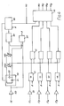
- Figure s 4 and 5 show a circuit for reading codes in accordance with the present invention.
- the circuit has five inputs 16,17,, 17 2 , 17 4 and 17 8 corresponding to the five columns on coding layer 15.
- the circuitry associated with inputs 17 2 , 17 4 and 17 8 is similar to that associated with input 17 1 , and will not be described in detail.
- the signals at inputs 16,17 1 are applied to respective non-linear amplifiers 40,41 which have a gain of 10 for induced input e.m.f.s. greater than a predetermined reference level and a gain of 1 for e.m.f.s. less than the reference level.
- the output of amplifier 40 is supplied to a clock track pulse sampler 50 which incorporates a first capacitor Cl for storing the clock pulse voltage and a second capacitor C2.
- the output of amplifier 40 is also applied to an input of a clock pulse detector 60.
- Outputs from sampler 50 are applied across potentiometers VR2 and VR1 each of which have a value of lOOKohm.
- An output from potentiometer VR1 is supplied to a second input of the clock pulse detector 60.
- a zero detector 65 is also connected to sampler 50 and is arranged to produce a reset signal R.
- the clock pulse detector 60 supplies an output to a pulse control logic circuit 80.
- Circuit 80 also receives the reset signal R from zero detector 65.
- Outputs of the logic circuit 80 are connected to the clock pulse sampler 50 and to a clock input of a data latch 70.
- the output of amplifier 41 is supplied to the first input of a data track pulse sampler 51, the second input of which is the reset signal from zero detector 65.
- Data pulse sampler 51 incorporates a capacitor for storing the peak level attained by voltage 17 1 .
- the output of sampler 51 is connected to a first input of a data pulse detector 61, the second input of which is the output of potentiometer VR2.
- the output of the data pulse detector 61 is connected to a respective data input of the data latch 70, which has a corresponding data output 95 1 .
- the four data outputs 95 1 , 95 2 , 95 4 and 95 8 may be connected to a microprocessor or digital hardware for further processing and/or to an LCD or similar display.
- the data may also be stored for later transmission, e.g. over modem link to a main frame computer.
- Software and/or hardware checks are used for CRC and word-length checking so that errors caused, for example, by not completing the reading stroke are flagged and cause a warning device to sound
- the peak level from the data track sampler 51 is compared in data detector 61 with a proportion (set by potentiometer VR2) of the clock track peak level.
- the condition "data hole present” or “data hole absent” is determined by the data track level being greater or less than this proportion respectively.
- Latching of the output of detector 61 into the data latch 70 occurs when the clock track level falls below a proportion (set by potentiometer VRl) of its peak level. Latching is effected by logic circuit 80 supplying a data pulse to the clock input of data latch 70. The data pulse also appears at an output 90 of the circuit.
- capacitors Cl and C2 and the associated logic circuitry function are fed to an input differential amplifier 150 of the clock pulse sampler 50.
- a diode 250 connected to the output of amplifier 150 the voltage on capacitor Cl can follow the input voltage upwards but not downwards.
- Capacitors Cl and C2 which are of equal value e.g. 10 microfarads, are interconnected via analogue switches 200,300.
- the logic circuitry 80 comprises two interconnected latch devices 180, 280 and the control inputs of the analogue switches 200,300 are connected to the Q and Q outputs of latch device 280, so that either switch 200 is on and switch 300 is off or switch 200 is off and switch 300 is on.
- switch 200 is off and C2 is shorted by switch 300.
- Cl charges up to the clock peak level voltage.
- switch 300 is off and switch 200 is on, which causes the voltage on Cl to be shared equally with C2; thus the voltage supplied to potentiometer VR1 falls to half the clock track peak level value.
- a fraction k of this half-value is compared at the clock pulse detector 60 with the clock input signal from amplifier 40.
- detector 60 acts as a threshold device and is used to determine whether the next clock pulse is present or not.
- the input signal rises through the "zero" level set by detector 65.
- the zero level used corresponds to a small positive voltage.
- the reset signal R applied, inter alia, to latch 180 to go from logic value 1 to logic value 0 (i.e high to low).
- the reset input of latch 280 which is connected to zero detector 65 via an inverting amplifier 165, goes from 0 to 1 which causes the output Q of latch 280 to go low, which switches off analogue switch 200, and output Q of latch 280 to go high, which switches on analogue switch 300 and thus discharges capacitor C2.
- the potentiometer VR1 supplies a voltage K x p/2 to an input of clock pulse detector 60, where k is less than 1.
- the clock pulse next reaches the val'ue p/2.
- the capacitor Cl then begins to charge up from p/2 to p, and the output of potentiometer VRl correspondingly rises from K x p/2 to K x p.
- the reset signal is withdrawn from the reset input of latch 280.
- An advantage of the above described arrangement is that it takes into account the speed dependence of the data track voltages by comparing them with a clock track voltage which has the same speed dependence.
- the use in this way of the induced levels for the clock track as a reference for the data tracks ensures that a wide range of speeds may be covered from 0.5 ft/sec (15 cm/sec) to the fastest possible that the reaching head can be physically moved by a person over a coded member.
- the layer 15 may be of any ferromagnetic material regardless of internal loss factor.
- the above-described arrangement is especially suitable for reading coded members attached to stationary railway wagons, the reading head being moved manually across the coded member.
- a fixed head may read coded members attached to wagons which are moving past.
- capacitors Cl and C2 may have different values.
- the above references to "half" the voltage level should be suitably modified.
- the values of Cl and C2 do not differ by more than a factor of two.
- the clock track 16 is at the edge in the coded member shown in Figs 1 and 2, it may, of course, be at any location across the member.
- the clock track constitutes the central column of holes, since this provides the option of having a symmetrical label which can be read in any direction, upside down and/or back to front.
- the data holes do not need to be duplicated in this modification. Rather the final data-detecting means is capable of determining that the information has been received in a particular form (e.g. back-to-front) and, e.g. by suitable programming, processing the information correctly.
- the arrangement of the present invention has the advantage that the arrangement will still function if the coded member and/or the reading head are covered with a thin layer of dirt since the magnitudes of the reference and data track signals will be affected to a similar extent. With all methods of coding the arrangement of the present invention also similarly compensates for differences in the separation of successive coded members from the reading head.
Landscapes
- Engineering & Computer Science (AREA)
- Artificial Intelligence (AREA)
- Computer Vision & Pattern Recognition (AREA)
- Physics & Mathematics (AREA)
- General Physics & Mathematics (AREA)
- Theoretical Computer Science (AREA)
- Signal Processing For Digital Recording And Reproducing (AREA)
Applications Claiming Priority (2)
| Application Number | Priority Date | Filing Date | Title |
|---|---|---|---|
| GB838315600A GB8315600D0 (en) | 1983-06-07 | 1983-06-07 | Coded reading arrangement |
| GB8315600 | 1983-06-07 |
Publications (1)
| Publication Number | Publication Date |
|---|---|
| EP0128752A2 true EP0128752A2 (de) | 1984-12-19 |
Family
ID=10543914
Family Applications (1)
| Application Number | Title | Priority Date | Filing Date |
|---|---|---|---|
| EP19840303867 Withdrawn EP0128752A2 (de) | 1983-06-07 | 1984-06-07 | Anordnungen zum Ablesen von Kodes |
Country Status (3)
| Country | Link |
|---|---|
| EP (1) | EP0128752A2 (de) |
| JP (1) | JPS6045977A (de) |
| GB (2) | GB8315600D0 (de) |
-
1983
- 1983-06-07 GB GB838315600A patent/GB8315600D0/en active Pending
-
1984
- 1984-06-07 EP EP19840303867 patent/EP0128752A2/de not_active Withdrawn
- 1984-06-07 GB GB08414550A patent/GB2141852A/en not_active Withdrawn
- 1984-06-07 JP JP11741884A patent/JPS6045977A/ja active Pending
Also Published As
| Publication number | Publication date |
|---|---|
| GB8414550D0 (en) | 1984-07-11 |
| JPS6045977A (ja) | 1985-03-12 |
| GB8315600D0 (en) | 1983-07-13 |
| GB2141852A (en) | 1985-01-03 |
Similar Documents
| Publication | Publication Date | Title |
|---|---|---|
| CA2049040C (en) | Magnetic code reader with adjustable thresholds | |
| EP0286378A2 (de) | Beglaubigungsverfahren und -systeme | |
| US3847346A (en) | Data field recognition and reading method and system | |
| US5285328A (en) | Process for evaluating binary data of a magnetic storage card using curve patterns | |
| US4218612A (en) | Magnetic signal detector | |
| US4354208A (en) | Magnetic recording medium and digital storage device including same | |
| US4232216A (en) | Method and device for reading coded information in the form of intervals of predetermined sizes | |
| CA2201306C (en) | Security thread detector assembly | |
| US4182481A (en) | Bar code reading device | |
| US3638238A (en) | Magnetic ink symbol recognition system with waveshapes representing direct magnetic flux | |
| US3715738A (en) | Data detection system | |
| US5736722A (en) | Dual sensor decoder | |
| US4328519A (en) | Reading secure magnetic documents | |
| EP0128752A2 (de) | Anordnungen zum Ablesen von Kodes | |
| US4414831A (en) | Key-operated lock | |
| CA1068387A (en) | Electronic railroad track marker system | |
| US3688260A (en) | Self-clocking digital data systems employing data-comparison codes and error detection | |
| EP0042707A1 (de) | Identitätsplakettenabtaster | |
| US5350950A (en) | Setting circuit of binary threshold value | |
| US4878136A (en) | Track crossing detector | |
| EP1204944B1 (de) | Verfahren zum lesen eines codierten etiketts | |
| Adams | Success and failure analysis of neurel network identification of aircraft noise | |
| EP0658267B1 (de) | Verarbeitung von aufgezeichneten daten | |
| JPS57189382A (en) | Discriminating method for information recording track | |
| EP0361488A3 (de) | Magnetisches Plattengerät mit einer Schaltungsanordnung zur Detektion von auf einer magnetischen Platte aufgezeichneten Servo-Informationen |
Legal Events
| Date | Code | Title | Description |
|---|---|---|---|
| PUAI | Public reference made under article 153(3) epc to a published international application that has entered the european phase |
Free format text: ORIGINAL CODE: 0009012 |
|
| AK | Designated contracting states |
Designated state(s): AT BE CH DE FR IT LI LU NL SE |
|
| STAA | Information on the status of an ep patent application or granted ep patent |
Free format text: STATUS: THE APPLICATION HAS BEEN WITHDRAWN |
|
| 18W | Application withdrawn |
Withdrawal date: 19850219 |
|
| RIN1 | Information on inventor provided before grant (corrected) |
Inventor name: PARSONS, LAURENCE EDWARD Inventor name: GALE, KENNETH CHARLES |