EP0126759B1 - Apparatus for deriving synchronisation signals for component television video signal reception - Google Patents
Apparatus for deriving synchronisation signals for component television video signal reception Download PDFInfo
- Publication number
- EP0126759B1 EP0126759B1 EP84900082A EP84900082A EP0126759B1 EP 0126759 B1 EP0126759 B1 EP 0126759B1 EP 84900082 A EP84900082 A EP 84900082A EP 84900082 A EP84900082 A EP 84900082A EP 0126759 B1 EP0126759 B1 EP 0126759B1
- Authority
- EP
- European Patent Office
- Prior art keywords
- signals
- frame
- line
- signal
- synchronisation
- Prior art date
- Legal status (The legal status is an assumption and is not a legal conclusion. Google has not performed a legal analysis and makes no representation as to the accuracy of the status listed.)
- Expired
Links
Images



Classifications
-
- H—ELECTRICITY
- H04—ELECTRIC COMMUNICATION TECHNIQUE
- H04N—PICTORIAL COMMUNICATION, e.g. TELEVISION
- H04N7/00—Television systems
- H04N7/08—Systems for the simultaneous or sequential transmission of more than one television signal, e.g. additional information signals, the signals occupying wholly or partially the same frequency band, e.g. by time division
- H04N7/083—Systems for the simultaneous or sequential transmission of more than one television signal, e.g. additional information signals, the signals occupying wholly or partially the same frequency band, e.g. by time division with signal insertion during the vertical and the horizontal blanking interval, e.g. MAC data signals
-
- H—ELECTRICITY
- H04—ELECTRIC COMMUNICATION TECHNIQUE
- H04N—PICTORIAL COMMUNICATION, e.g. TELEVISION
- H04N11/00—Colour television systems
- H04N11/06—Transmission systems characterised by the manner in which the individual colour picture signal components are combined
- H04N11/08—Transmission systems characterised by the manner in which the individual colour picture signal components are combined using sequential signals only
-
- H—ELECTRICITY
- H04—ELECTRIC COMMUNICATION TECHNIQUE
- H04N—PICTORIAL COMMUNICATION, e.g. TELEVISION
- H04N9/00—Details of colour television systems
- H04N9/44—Colour synchronisation
Definitions
- the present invention relates to a system for transmitting and/or receiving television video signals in component form, which components have been time compressed and placed sequentially so as to occupy, together with the necessary sync and clamping signals, a period substantially identical to the existing line period, e.g. approximately 64 ⁇ S.
- this audio signal takes the form of a digital signal placed before the video components signals. Further, it has been proposed to add to this digital signal a predetermined sequence of digits for use as either a sound or line sync signal.
- sequences there will be just two predetermined sequences which will alternate line by line for the bulk of one frame but-one of the sequences will be repeated for a plurality of lines just prior to the end of one frame while the other of the sequences will be repeated for a plurality of lines at the beginning of the next frame.
- the sequences will then alternate as before.
- the present invention provides a method for deriving line and frame frequency synchronisation signals from a received television signal which has a repeated sequence for a plurality of different digital words, each word in a respective one of a plurality of lines, as synchronisation signals comprising the steps:
- the present invention further provides apparatus for deriving line and frame frequency synchronisation signals from a received television signal which has a repeated sequence of a plurality of different digital words, each word in a respective one of a plurality of lines, as synchronisation signals comprising
- the Multiplex Analogue Components (MAC) system for whom television signal transmission replaces the colour subcarrier coding of NTSC, PAL and SECAM with a single method of time compression.
- the conventional studio colour coder is replaced by a MAC coder which separately time compresses each active picture line (52 ps nominally) of luminance (Y) and chrominance (alternate lines contain U and V).
- Y luminance
- chrominance alternate lines contain U and V
- CCDs charge-coupled devices
- Conventional sync pulses designed for receiver technology over 30 years ago, are no longer required and are replaced by other synchronisatioon information within the waveform.
- the colour subcarrier burst is no longer required, and any timing information required for further developments such as extended definition receivers can be derived from the video and sound/data signals.
- This time compression results in a proportionate increase in the bandwith required to pass the signal.
- the extra bandwidth of the time-compressed baseband signal can be accommodated within a satellite FM transmission channel, since the spectral width of the FM signal is a function of both the frequency and amplitude of the baseband signals.
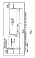
- the synchronisation, sound and data signals are digitally modulated onto the carrier in the line-blanking interval of the MAC signal, giving an overall time division multiplex of the RF carrier as shown in Fig. 1.
- the complete absence of high frequency sub-carriers either for colour or for sound allows the bandwidth of the baseband signals to be increased with the upper limit set by interference constraints.
- the use of large amounts of pre- and de-emphasis to reduce distortion on subcarriers becomes unnecessary. As a result, the pre- and de-emphasis can be reduced to a level to give optimum noise and interference performance.
- Time division multiplexing of the digital synchronisation, sound and data with the analogue video signal is carried out at an intermediate frequency, switching between digital modulation for the ⁇ synchronisation, sound and data, and frequency modulation from the chrominance and luminance as shown in Figure 1. Such switching is carried out without discontinuity of phase in the main carrier.
- Luminance compression of 1.5:1 and chrominance compression 3:1 which are used for C-MAC mean that after compression the effective sampling frequencies for both luminance and chrominance are 20.25 MHz. For convenience of generation and recovery, the same data rate is chosen for the sound signal.
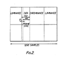
- Fig. 2 shows the format of a C-MAC signal offset by line and frame.
- the line is broken into the three component parts of the time division multiplex as shown in Table 1.
- line synchronising words W, and W 2 which are sent on alternate lines. Their relative positions are inverted once every frame to provide a frame reference as shown in Table 2 below.
- the line sync word W 2 is replaced with a 7 bit word which may be used for signalling purposes.
- Line syncs may also be derived by detecting a unique frame sync word placed in line 625 as shown in Fig. 2 and using this to lock an oscillator running at line rate.
- Video frame sync This is available in two ways:
- the synchronisation period consists of an 8-bit sequence transmitted at the start of each data burst. Of this the first bit is a run-in bit, and without synchronisation detection can be considered to be of no useful value.
- the other seven bits contain both the horizontal and vertical sync information in the format shown below.
- a line sync can be considered to consist of either the word pair W, W 2 or the pair W 2 W 1 .
- a frame sync will then consist of the sequences W, W 1 W 2 W 2 or W 2 W 2 W 1 W, reversing a W 1 W 2 pair at the frame boundary.
- W 1 , W 2 The choice of words for W 1 , W 2 is governed solely by the desired behaviour of the system under conditions of noise.
- Both W, and W 2 should be chosen to have smallest possible correlation with shifted versions of themselves to prevent false lock occurring.
- W 2 was chosen to be 1110010.
- a line sync is therefore present on every line and a frame sync once a frame.
- the line marked t contains a valid line sync, but the W 1 W 2 pair sequence is inverted. This can be used as a less rugged form of frame sync if desired for a simpler receiver and is indicated in Fig. 2.
- a phase locked loop recovers the 20.25 MHz clock from the incoming data stream in a conventional manner. Even when not locked, the oscillator of the phase locked loop is running at a nominal 20.25 MHz and so there is only scale difference in phase between the incoming data stream and the oscillator which results in long period of in phase running of the oscillator in facilitate lock-up.
- a sync word recognition circuit 21 which converts the continuous 20 Mb/s data stream to a continuous error pattern. That is, the output represents the number of bits that the input is away from W 1 . For example, in the case of W 2 this is the Hamming distance, or 7.
- the figure e l may be used as a measure of the BER for the channel.
- This operation is achieved by means of an inverter 22 which inverts the present sample and feeds it to one input of an adder 23 whose other input is supplied with the output from a line delay circuit 24.
- the output of the adder 23 is fed to a comparing circuit 25 where the 4 bit output of the adder 23 is compared with predetermined maximum and minimum numbers of errors and if the level of the output of the adder 23 falls between the maximum and minimum numbers of errors a line sync detection signal is generated.
- a frame sync signal could also be extracted from the circuit 25 by detection when minimum and maximum signals are produced.
- the uninverted present sample is in this case summed with the same sample from the previous line in an adder 27. This gives a minimum for W, W, and a maximum for the sequence W 2 W 2 . This result is delayed by two lines in a delay circuit 28 which comprises a 2 x 4 bit 2 line gated latch and added to the inverted undelayed signal in an adder 30.
- False sync pulses may also be generated by the random data in the channel, or by a particular arrangement of video signals. Therefore some sort of discrimination is required to extract the true syncs from any possible misdetections.
- the clock recovery PLL is gated to prevent spurious signals (e.g.g video) outside the burst increasing the amount of jitter on the clock.
- the state diagram is the same for line and frame syncs, but acquisition of frame sync is not initiated until line lock is acquired when the position of frame sync can be indicated by line syncs.
- Clock recovery is gated as soon as line lock is established (3 lines) thereby reducing clock jitter at low C/N.
- the clock has only to run ungated for 3 lines as opposed to running ungated accurately for at least one frame.
- Figure 5 shows a block diagram of a part of a receiver concentrating on sync detection and acquisition which differs from that shown in Fig. 3 in that it is much more simple and easy to instruct.
- the previously described receiver required a fairly substantial amount of hardware, mostly running at the 20.25 Mb/s clock rate.
- the receiver shown in Figure 5 and described below has a considerably reduced amount of logic running at 20.25 MHz and in particular contains no line store.
- the same reference numerals are used for the same parts as in Fig. 3.
- serial incoming data is inverted as before in a circuit 40 to produce a 3-bit error word.
- a line sync acquisition and flywheel and state counter circuit 41 receives an input from a word detection circuit each time a W 1 or W 2 word is detected by a word detection circuit 42 connected to the output of the circuit 40. It also receives the line sync detection signal generated by the comparing circuit 25.
- the counter circuit 41 generates a number of outputs among which is a line rate clock signal which is fed to a 3-bit latch 43 which replaces the line delay circuit 24 of Fig. 3.
- the counter circuit 41 also acts as a reference signal generator for generating reference signals for application to a word detector and adaptive error control circuit 44.
- the reference signal being used to select the type of detection and number of errors tolerated by the detector 42 and the comparing circuit 25.
- Adaptive error control is achieved using a frame sync flywheel and acquisition circuit 46 and an error control circuit 47 which operates in a similar manner to the corresponding circuits described in relation to line sync detector.
- the counter circuit 41 is now at state 2 in ( Figure 3A).
- Frame syncs are detected using a 2 latch double line delay as before, and frame lock is also acquired as before.
- Adaptive error tolerance on either or both line and frame sync detection allows sync extraction in the presence of a greater amount of noise (or higher BER).
- the arrangement shown in Fig. 5 has an increased initial lock up time with respect to that of Fig. 3. This is increased by an average of 12 lines in low BER conditions to approximately 40 lines at a BER of 10- 1 .
Landscapes
- Engineering & Computer Science (AREA)
- Multimedia (AREA)
- Signal Processing (AREA)
- Power Engineering (AREA)
- Synchronisation In Digital Transmission Systems (AREA)
- Television Systems (AREA)
- Synchronizing For Television (AREA)
- Processing Of Color Television Signals (AREA)
Abstract
Description
- The present invention relates to a system for transmitting and/or receiving television video signals in component form, which components have been time compressed and placed sequentially so as to occupy, together with the necessary sync and clamping signals, a period substantially identical to the existing line period, e.g. approximately 64 µS.
- It has already been proposed to compress the video component signals to such an extent that an audio signal can be included either before or after the video component signal, within the line period. It is preferred that this audio signal takes the form of a digital signal placed before the video components signals. Further, it has been proposed to add to this digital signal a predetermined sequence of digits for use as either a sound or line sync signal.
- We now propose that a plurality of predetermined digital sequences be used, each in a different line, from which both line and frame syncs may be derived in a receiving apparatus.
- Preferably, there will be just two predetermined sequences which will alternate line by line for the bulk of one frame but-one of the sequences will be repeated for a plurality of lines just prior to the end of one frame while the other of the sequences will be repeated for a plurality of lines at the beginning of the next frame. The sequences will then alternate as before.
- The present invention provides a method for deriving line and frame frequency synchronisation signals from a received television signal which has a repeated sequence for a plurality of different digital words, each word in a respective one of a plurality of lines, as synchronisation signals comprising the steps:
- a) recognising one of the digital words;
- b) generating a first signal indicative of recognition of said one of the digital words;
- c) recognising at least one further digitial word;
- d) generating at least one further signal indicative of recognition of a respective further digital word;
- e) operating on the first and further signals to determine the sequence and timing of the first and further signals whereby to generate a signal indicative of synchronisation signal detection; and
- f) initiating the generation of receiver sync signals at the line and frame frequency in response to the signal produced as a result of the operating step.
- The present invention further provides apparatus for deriving line and frame frequency synchronisation signals from a received television signal which has a repeated sequence of a plurality of different digital words, each word in a respective one of a plurality of lines, as synchronisation signals comprising
- means (21) for generating a first signal indicative of recognition of one of the digital words;
- means (21) for generating at least one further signal indicative of recognition of a respective further digital word; and
- means (22, 23, 24, 25, 27, 28, 30, 31) for operating on the first and further signals to determine the sequence and timing of the first and further signals whereby to generate a signal indicative of synchronisation signal detection for initiating generation of receiver sync signals at the line and frame frequency.
- In order that the present invention be more readily understood, reference will now be made to the accompanying drawings, in which:
- Figure 1 shows diagrammatically a multiplexed component signal showing the time division multiplex between the components parts thereof;
- Figure 2 shows diagrammatically a frame of C-MAC signals offset by frame and line as well as the multiple timing of each line in the frame. 4
- Figure 3 shows a block diagram of a receiver incorporating the present invention.
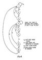
- Figure 4 shows a state diagram to explain the operation of the circuit shown in Figure 3.
- Figure 5 shows a block diagram of a further receiver incorporating the present invention; and
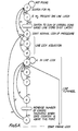
- Figure 6A and 6B show state diagrams to explain the operation of the circuit shown in Figure 5.
- The Multiplex Analogue Components (MAC) system for whom television signal transmission replaces the colour subcarrier coding of NTSC, PAL and SECAM with a single method of time compression. The conventional studio colour coder is replaced by a MAC coder which separately time compresses each active picture line (52 ps nominally) of luminance (Y) and chrominance (alternate lines contain U and V). By using either charge-coupled devices (ie CCDs) or digital storage, these compressed luminance and chrominance components can be placed in sequence within the 64 µs of each line period. Conventional sync pulses, designed for receiver technology over 30 years ago, are no longer required and are replaced by other synchronisatioon information within the waveform. The colour subcarrier burst is no longer required, and any timing information required for further developments such as extended definition receivers can be derived from the video and sound/data signals.
- This time compression results in a proportionate increase in the bandwith required to pass the signal. The extra bandwidth of the time-compressed baseband signal can be accommodated within a satellite FM transmission channel, since the spectral width of the FM signal is a function of both the frequency and amplitude of the baseband signals.
- In one version of MAC known as C-MAC, the synchronisation, sound and data signals are digitally modulated onto the carrier in the line-blanking interval of the MAC signal, giving an overall time division multiplex of the RF carrier as shown in Fig. 1. The complete absence of high frequency sub-carriers either for colour or for sound allows the bandwidth of the baseband signals to be increased with the upper limit set by interference constraints. The use of large amounts of pre- and de-emphasis to reduce distortion on subcarriers becomes unnecessary. As a result, the pre- and de-emphasis can be reduced to a level to give optimum noise and interference performance.
- Time division multiplexing of the digital synchronisation, sound and data with the analogue video signal is carried out at an intermediate frequency, switching between digital modulation for the ` synchronisation, sound and data, and frequency modulation from the chrominance and luminance as shown in Figure 1. Such switching is carried out without discontinuity of phase in the main carrier.
- The internationally agreed studio standard for component-coded digital video has been established with sampling frequencies 13.5 MHz for luminance and 6.75 MHz for chrominance. Luminance compression of 1.5:1 and chrominance compression 3:1 which are used for C-MAC mean that after compression the effective sampling frequencies for both luminance and chrominance are 20.25 MHz. For convenience of generation and recovery, the same data rate is chosen for the sound signal.
- In defining the waveform, it is convenient to divide the 64 psec video line into 1296 time slots or 'samples' based on integer periods of 49.4 nsec (1/20.25 MHz) which are shown in Fig. 2 which shows the format of a C-MAC signal offset by line and frame.
- On this basis, the line is broken into the three component parts of the time division multiplex as shown in Table 1.


- Signalling bits. On 20 lines of each frame, the line sync word W2 is replaced with a 7 bit word which may be used for signalling purposes.
- These lines are as follows;
- Even frames- line 26, 58, 74, 90, 152,182,198, 216, 276, 308, 324, 340, 400, 432, 458, 466, 526, 558, 574, 590.
- Odd frames-
line 27, 59, 75, 91,153, 183,199, 217, 277, 309, 325, 341, 401, 433, 459, 467, 527, 559, 575, 591. - Even and odd frames are defined in Table 2.
- b) Line syncs may also be derived by detecting a unique frame sync word placed in line 625 as shown in Fig. 2 and using this to lock an oscillator running at line rate.
- ii) Video frame sync: This is available in two ways:
- a) From the digital burst. The first 8 bits of the digital burst provide not only the line syncs, but by inversion of the relative positions of the words once every frame a rugged frame sync is provided as shown in Table 2 above.
- b) Alternatively, a distinct and unique frame sync word can be inserted in line 625 as shown in Fig. 2. iii) U/V identification. The UN identitication is derived directly by line count from the frame sync. The odd lines of the frame carry U information and the even lines carry V information.
- iv) Extended definition synchronisation. For extended processing which may be introduced in the future, the 20.25 MHz clock required is recovered from the sound data burst.
- v) Sound synchronisation. Sound synchronisation is obtained by obtaining line and frame synchronisation from the digital burst which then provides total synchronisation of the sound/data channel.
- Turning now to the generation of sync signals at the receiver from the C-MAC waveform shown in Fig. 1, it will be recalled that the timings for the MAC receiver are derived from a line-locked 20.25 MHz clock. This has a period of =49 nS, and there are 1296 clock samples per television line. As timing information for clock regeneration is derived from the data burst, it can be seen that timing information is only present for 15% of the time.
- The synchronisation period consists of an 8-bit sequence transmitted at the start of each data burst. Of this the first bit is a run-in bit, and without synchronisation detection can be considered to be of no useful value. The other seven bits contain both the horizontal and vertical sync information in the format shown below.
- From Table 2 it will be appreciated that a line sync can be considered to consist of either the word pair W, W2 or the pair W2 W1.
- A frame sync will then consist of the sequences W, W1 W2 W2 or W2 W2 W1 W, reversing a W1 W2 pair at the frame boundary.
- The choice of words for W1, W2 is governed solely by the desired behaviour of the system under conditions of noise.
- Both W, and W2 should be chosen to have smallest possible correlation with shifted versions of themselves to prevent false lock occurring.
- Based on computer search, the seven bit seqeuence 0001101 has been found to be optimum with regard to shifted versions of itself and also simulation of the sequence by video/data and noise.
- In order to prevent confusion between W, and W2 occurring in the receiver, a large Hamming distance between the two is desirable, and hence W2 was chosen to be 1110010.
- To keep the average D.C. level to

- Although only seven bits of sync information are sent on each line, the sequence of W1 W2 allows an effective line sync word length of 14 bits and an effective frame sync word length of 28 bits to be used. This is shown below:-
-

- A line sync is therefore present on every line and a frame sync once a frame.
- On the lines marked * a line sync is not detected due to the W, W2 pair inversion to signal a frame sync. The ability of the system to stay in lock is not affected because the line sync detection is inhibited during these two lines once a frame lock is established.
- The line marked t contains a valid line sync, but the W1 W2 pair sequence is inverted. This can be used as a less rugged form of frame sync if desired for a simpler receiver and is indicated in Fig. 2.
- A block diagram of the receiver detector is shown below in Figure 3, and a brief description of the operation follows.
- A phase locked loop (not shown) recovers the 20.25 MHz clock from the incoming data stream in a conventional manner. Even when not locked, the oscillator of the phase locked loop is running at a nominal 20.25 MHz and so there is only scale difference in phase between the incoming data stream and the oscillator which results in long period of in phase running of the oscillator in facilitate lock-up.
- The input serial data stream is then converted to an n bit wide parallel data stream by a serial to
parallel converter 20, where n is the width of the line sync (i.e. n = 7). - This is processed by a sync
word recognition circuit 21 which converts the continuous 20 Mb/s data stream to a continuous error pattern. That is, the output represents the number of bits that the input is away from W1. For example, in the case of W2 this is the Hamming distance, or 7. - Since e-W2 =
e W 2, by inverting the present sample and summing this with the same sample from the previous line, a maximum will occur with the line pair W, W2 and a minimum with the pair W2 W,. By comparing these with eamin and eamax (the number of errors allowed in a sync word pair before a detection is deemed to be missed) line syncs may be extracted (along with other false detections due to random data) from the input data stream. - The figureel may be used as a measure of the BER for the channel.
- This operation is achieved by means of an
inverter 22 which inverts the present sample and feeds it to one input of anadder 23 whose other input is supplied with the output from aline delay circuit 24. The output of theadder 23 is fed to a comparingcircuit 25 where the 4 bit output of theadder 23 is compared with predetermined maximum and minimum numbers of errors and if the level of the output of theadder 23 falls between the maximum and minimum numbers of errors a line sync detection signal is generated. - A frame sync signal could also be extracted from the
circuit 25 by detection when minimum and maximum signals are produced. - This is preferably performed in a manner similar to line syncs with one important difference. The uninverted present sample is in this case summed with the same sample from the previous line in an
adder 27. This gives a minimum for W, W, and a maximum for the sequence W2 W2. This result is delayed by two lines in adelay circuit 28 which comprises a 2 x 4bit 2 line gated latch and added to the inverted undelayed signal in anadder 30. - Again this result has a minimum for W2 W2 W, W, and a maximum for W, W1 W2 W2. By using a
comparison circuit 31 for comparing this result with the number of errors allowable before a detection is not signalled, frame syncs may be detected. - The significant difference between frame sync and line sync extraction is the two
line delay circuit 28. This is simply a two element shift register clocked with the regenerated line sync. - Once line lock has been established, the precise horizontal position of the frame sync within one of only 625 possible positions. It is effectively 'pointed to' by the line syncs. Hence the frame sync is made much more robust. This contrasts with a system using a frame sync word only i.e. where the frame sync may be in one of 625 x 1296 locations.
- The previous section described in the recovery of the sync pulses. False sync pulses may also be generated by the random data in the channel, or by a particular arrangement of video signals. Therefore some sort of discrimination is required to extract the true syncs from any possible misdetections.
- The process by which lock is acquired is governed by the state diagram shown in Fig. 4.
- In the initial state any detection of the sync word is accepted, and a counter connected to the output of the comparing
circuit 25 is moved tostate 2 . - If this detection is not the sync word then the counter returns to
state 1. - If it is the sync word, the counter progresses to
state 4 and the system has acquired lock. - Once line syncs have been acquired, the position of the data burst is known with certainty, and the clock recovery PLL is gated to prevent spurious signals (e.g.g video) outside the burst increasing the amount of jitter on the clock.
- After 16 consecutive mis-detections the system reverts to
state 1 and has lost lock. - The state diagram is the same for line and frame syncs, but acquisition of frame sync is not initiated until line lock is acquired when the position of frame sync can be indicated by line syncs.
- The figures in this diagram allow lock to be acquired and held at a C/N of O dB in the UKIBA C-MAC system. This has been confirmed by experimental results.
- Sync acquisition is thus by two distinct processes:-
- 1) Detection of line and frame sync.
- 2) Lock acquisition and digital flywheeling.
- Clock recovery is gated as soon as line lock is established (3 lines) thereby reducing clock jitter at low C/N. The clock has only to run ungated for 3 lines as opposed to running ungated accurately for at least one frame.
- Figure 5 shows a block diagram of a part of a receiver concentrating on sync detection and acquisition which differs from that shown in Fig. 3 in that it is much more simple and easy to instruct.
- The previously described receiver required a fairly substantial amount of hardware, mostly running at the 20.25 Mb/s clock rate.
- The receiver shown in Figure 5 and described below has a considerably reduced amount of logic running at 20.25 MHz and in particular contains no line store. The same reference numerals are used for the same parts as in Fig. 3.
- In Fig. 5, serial incoming data is inverted as before in a
circuit 40 to produce a 3-bit error word. A line sync acquisition and flywheel andstate counter circuit 41 receives an input from a word detection circuit each time a W1 or W2 word is detected by aword detection circuit 42 connected to the output of thecircuit 40. It also receives the line sync detection signal generated by the comparingcircuit 25. Thecounter circuit 41 generates a number of outputs among which is a line rate clock signal which is fed to a 3-bit latch 43 which replaces theline delay circuit 24 of Fig. 3. - The
counter circuit 41 also acts as a reference signal generator for generating reference signals for application to a word detector and adaptiveerror control circuit 44. The reference signal being used to select the type of detection and number of errors tolerated by thedetector 42 and the comparingcircuit 25. - For frame sync detection, the arrangement is as described in relation to Fig. 3 with the 2
line delay 28 responsive to the line rate clock now generated by thecounter circuit 41. Adaptive error control is achieved using a frame sync flywheel andacquisition circuit 46 and anerror control circuit 47 which operates in a similar manner to the corresponding circuits described in relation to line sync detector. - The process of line sync acquisition will now be described with reference to Fig. 5 and Figs. 6A and 6B.
- Initially search for W, (only W, detections are output from a comparator on the output of the serial to error
converter 40, allowing n errors). - If W, is found, the
counter circuit 41 moves to state 1 (Figure 3A) and searches for an occurrence of W2 precisely 1296 clock cycles (1 line) later. This is also output from theword recognition circuit 42 since W, = Wz. - If W2 is not found, the
counter circuit 41 reverts to state 0 (Figure 3A) and continues to search for another occurrence of W,. - If W2 is found, then the probability of having found a line sync pair is quite high, and the receiver switches over to the sum of errors mode of the previoous receiver, except that in this case, the line store is replaced by 3-
bit latch 43 clocked by the assumed position of line sync found from the separate W., and W2 detections. - The
counter circuit 41 is now atstate 2 in (Figure 3A). - If the syncs were correctly identified then the conventional locking procedure will be followed and the
counter circuit 41 will sit at state 5 (in Figure 3A) and the receiver will have acquired line lock and a line sync output will be generated by thecircuit 41. - At this point, the search for frame lock is initiated and when frame sync is acquired a frame sync output is generated from the
circuit 46. - Frame syncs are detected using a 2 latch double line delay as before, and frame lock is also acquired as before.
- In both line and frame cases, increasing BER will increase the probability of sync detection being missed and hence the
counters circuits - Once frame lock is lost, re-acquisition takes place as normal.
- Once line lock is lost, instead of reverting to state zero, the
counter circuit 41 reverts tostate 2. - There are two reasons for loss of line lock - loss of signal, or m consecutive mis-detections due to noise.
- In the former case the
counter circuit 41 will return to state 0 viastate 2. - In the latter case, if sync words are detected there is the possibility of re-acquiring lock whilst still running in the two word mode thereby considerably reducing the interruption to sound and vision caused by loss of lock.
- Adaptive error tolerance on either or both line and frame sync detection, allows sync extraction in the presence of a greater amount of noise (or higher BER). The arrangement shown in Fig. 5 has an increased initial lock up time with respect to that of Fig. 3. This is increased by an average of 12 lines in low BER conditions to approximately 40 lines at a BER of 10-1.
- Although not shown in Figure 3, it will be appreciated that a modified version of the
counter circuit 41 in Figure 5 will be used and that adaptive error control of thecircuit 25 and/orcircuit 31 is possible.
Claims (18)
Priority Applications (1)
| Application Number | Priority Date | Filing Date | Title |
|---|---|---|---|
| AT84900082T ATE57289T1 (en) | 1982-12-02 | 1983-12-02 | SYNCHRONIZATION SIGNAL REMOVAL DEVICE FOR COMPONENT TELEVISION VIDEO SIGNAL RECEPTION. |
Applications Claiming Priority (6)
| Application Number | Priority Date | Filing Date | Title |
|---|---|---|---|
| GB8234340 | 1982-12-02 | ||
| GB8234340 | 1982-12-02 | ||
| GB8304446 | 1983-02-17 | ||
| GB838304446A GB8304446D0 (en) | 1983-02-17 | 1983-02-17 | Component television video signal transmission and reception |
| GB8316581 | 1983-06-17 | ||
| GB838316581A GB8316581D0 (en) | 1983-06-17 | 1983-06-17 | Component television video signal transmission and reception |
Publications (2)
| Publication Number | Publication Date |
|---|---|
| EP0126759A1 EP0126759A1 (en) | 1984-12-05 |
| EP0126759B1 true EP0126759B1 (en) | 1990-10-03 |
Family
ID=27261850
Family Applications (1)
| Application Number | Title | Priority Date | Filing Date |
|---|---|---|---|
| EP84900082A Expired EP0126759B1 (en) | 1982-12-02 | 1983-12-02 | Apparatus for deriving synchronisation signals for component television video signal reception |
Country Status (5)
| Country | Link |
|---|---|
| EP (1) | EP0126759B1 (en) |
| JP (1) | JPS59502167A (en) |
| AT (1) | ATE57289T1 (en) |
| DE (1) | DE3381927D1 (en) |
| WO (1) | WO1984002242A1 (en) |
Families Citing this family (8)
| Publication number | Priority date | Publication date | Assignee | Title |
|---|---|---|---|---|
| GB2174567A (en) * | 1985-04-29 | 1986-11-05 | Philips Electronic Associated | Deriving frame interval signals |
| DE3613798A1 (en) * | 1986-04-24 | 1987-10-29 | Grundig Emv | METHOD FOR PROCESSING TELEVISION SIGNALS |
| FR2605479B1 (en) * | 1986-10-17 | 1989-04-07 | Telediffusion Fse | SYSTEM FOR EXTRACTING FRAME SYNCHRONIZATION SIGNALS FROM PACKET SYNCHRONIZATION SIGNALS |
| DE3704456C1 (en) * | 1987-02-13 | 1987-11-19 | Rohde & Schwarz | Arrangement for displaying MAC signals on a monitor |
| DE3737730C2 (en) * | 1987-11-06 | 1995-10-26 | Broadcast Television Syst | Method and arrangement for deriving synchronous signals |
| DE3827106C1 (en) * | 1988-08-10 | 1989-05-03 | Richard Hirschmann Radiotechnisches Werk, 7300 Esslingen, De | |
| IT1227483B (en) * | 1988-11-23 | 1991-04-12 | Telettra Lab Telefon | SYSTEM AND DEVICES FOR THE TRANSMISSION OF SIGNALS CONSISTENT OF DATA BLOCKS |
| GB2245727A (en) * | 1990-06-18 | 1992-01-08 | Rank Cintel Ltd | Method and apparatus for generating timing signals |
-
1983
- 1983-12-02 DE DE8484900082T patent/DE3381927D1/en not_active Expired - Lifetime
- 1983-12-02 EP EP84900082A patent/EP0126759B1/en not_active Expired
- 1983-12-02 WO PCT/GB1983/000315 patent/WO1984002242A1/en not_active Ceased
- 1983-12-02 AT AT84900082T patent/ATE57289T1/en not_active IP Right Cessation
- 1983-12-02 JP JP84500105A patent/JPS59502167A/en active Pending
Also Published As
| Publication number | Publication date |
|---|---|
| WO1984002242A1 (en) | 1984-06-07 |
| EP0126759A1 (en) | 1984-12-05 |
| ATE57289T1 (en) | 1990-10-15 |
| DE3381927D1 (en) | 1990-11-08 |
| JPS59502167A (en) | 1984-12-27 |
Similar Documents
| Publication | Publication Date | Title |
|---|---|---|
| US4675722A (en) | Apparatus for deriving synchronization signals for component television video signal reception | |
| US4724486A (en) | Apparatus for deriving information signals for component television video signal reception | |
| US3984624A (en) | Video system for conveying digital and analog information | |
| US5940137A (en) | Symbol timing generation and recovery for data transmission in an analog video signal | |
| US6014416A (en) | Method and circuit for detecting data segment synchronizing signal in high-definition television | |
| US4688246A (en) | CATV scrambling system with compressed digital audio in synchronizing signal intervals | |
| US4707730A (en) | Sync extraction for a broadcasting system with time multiplexing of digital and analog signals | |
| KR0162603B1 (en) | Apparatus for processing ntsc tv signals having digital signals on quadrature phase video carrier | |
| CA1288520C (en) | Synchronization recovery in a communications system | |
| US5416524A (en) | Digital television synchronization system and method | |
| US4626913A (en) | Chroma burst derived clock regenerator for teletext decoder | |
| CA2226821C (en) | Vsb symbol sync recovery system | |
| US4636852A (en) | Scrambling and descrambling of television signals for subscription TV | |
| WO1984002242A1 (en) | Apparatus for deriving synchronisation signals for component television video signal reception | |
| KR0168676B1 (en) | Teletext signal separator | |
| US5323236A (en) | An extended television signal encoding and decoding system comprising control data for controlling the decoder | |
| US4829377A (en) | Horizontal synchronization, clock synchronization, D. C. restoration and gain control scheme for an analog TV system | |
| US4970592A (en) | Horizontal synchronization, clock synchronization, D.C. restoration and gain control scheme for an analog TV system | |
| US5196921A (en) | Data transmission using color burst position modulation | |
| KR0167899B1 (en) | Data Segment Synchronization Detection Circuit of High-Definition Television System | |
| RU2010452C1 (en) | Method and device for forming disturbances for pal and secam video signals | |
| JPS59117390A (en) | System for transmitting color television signal | |
| JPS60500113A (en) | Information signal extraction device for component television video signal reception | |
| JPH065895B2 (en) | Phase synchronization signal regenerator | |
| JPS6243634B2 (en) |
Legal Events
| Date | Code | Title | Description |
|---|---|---|---|
| PUAI | Public reference made under article 153(3) epc to a published international application that has entered the european phase |
Free format text: ORIGINAL CODE: 0009012 |
|
| 17P | Request for examination filed |
Effective date: 19840723 |
|
| AK | Designated contracting states |
Designated state(s): AT BE CH DE FR GB LI LU NL SE |
|
| GRAA | (expected) grant |
Free format text: ORIGINAL CODE: 0009210 |
|
| AK | Designated contracting states |
Kind code of ref document: B1 Designated state(s): AT BE CH DE FR GB LI LU NL SE |
|
| REF | Corresponds to: |
Ref document number: 57289 Country of ref document: AT Date of ref document: 19901015 Kind code of ref document: T |
|
| REF | Corresponds to: |
Ref document number: 3381927 Country of ref document: DE Date of ref document: 19901108 |
|
| ET | Fr: translation filed | ||
| PLBE | No opposition filed within time limit |
Free format text: ORIGINAL CODE: 0009261 |
|
| STAA | Information on the status of an ep patent application or granted ep patent |
Free format text: STATUS: NO OPPOSITION FILED WITHIN TIME LIMIT |
|
| 26N | No opposition filed | ||
| REG | Reference to a national code |
Ref country code: GB Ref legal event code: 732E |
|
| EPTA | Lu: last paid annual fee | ||
| EAL | Se: european patent in force in sweden |
Ref document number: 84900082.3 |
|
| REG | Reference to a national code |
Ref country code: GB Ref legal event code: 732E |
|
| REG | Reference to a national code |
Ref country code: GB Ref legal event code: 732E |
|
| REG | Reference to a national code |
Ref country code: GB Ref legal event code: IF02 |
|
| PGFP | Annual fee paid to national office [announced via postgrant information from national office to epo] |
Ref country code: LU Payment date: 20021024 Year of fee payment: 20 |
|
| PGFP | Annual fee paid to national office [announced via postgrant information from national office to epo] |
Ref country code: GB Payment date: 20021104 Year of fee payment: 20 Ref country code: AT Payment date: 20021104 Year of fee payment: 20 |
|
| PGFP | Annual fee paid to national office [announced via postgrant information from national office to epo] |
Ref country code: NL Payment date: 20021112 Year of fee payment: 20 |
|
| PGFP | Annual fee paid to national office [announced via postgrant information from national office to epo] |
Ref country code: FR Payment date: 20021202 Year of fee payment: 20 |
|
| PGFP | Annual fee paid to national office [announced via postgrant information from national office to epo] |
Ref country code: SE Payment date: 20021203 Year of fee payment: 20 |
|
| PGFP | Annual fee paid to national office [announced via postgrant information from national office to epo] |
Ref country code: CH Payment date: 20021223 Year of fee payment: 20 |
|
| PGFP | Annual fee paid to national office [announced via postgrant information from national office to epo] |
Ref country code: DE Payment date: 20021230 Year of fee payment: 20 |
|
| PGFP | Annual fee paid to national office [announced via postgrant information from national office to epo] |
Ref country code: BE Payment date: 20030116 Year of fee payment: 20 |
|
| PG25 | Lapsed in a contracting state [announced via postgrant information from national office to epo] |
Ref country code: LI Free format text: LAPSE BECAUSE OF EXPIRATION OF PROTECTION Effective date: 20031201 Ref country code: GB Free format text: LAPSE BECAUSE OF EXPIRATION OF PROTECTION Effective date: 20031201 Ref country code: CH Free format text: LAPSE BECAUSE OF EXPIRATION OF PROTECTION Effective date: 20031201 |
|
| PG25 | Lapsed in a contracting state [announced via postgrant information from national office to epo] |
Ref country code: NL Free format text: LAPSE BECAUSE OF EXPIRATION OF PROTECTION Effective date: 20031202 Ref country code: LU Free format text: LAPSE BECAUSE OF EXPIRATION OF PROTECTION Effective date: 20031202 Ref country code: AT Free format text: LAPSE BECAUSE OF EXPIRATION OF PROTECTION Effective date: 20031202 |
|
| REG | Reference to a national code |
Ref country code: GB Ref legal event code: PE20 |
|
| BE20 | Be: patent expired |
Owner name: *INDEPENDENT BROADCASTING AUTHORITY Effective date: 20031202 |
|
| REG | Reference to a national code |
Ref country code: CH Ref legal event code: PL |
|
| NLV7 | Nl: ceased due to reaching the maximum lifetime of a patent |
Effective date: 20031202 |
|
| EUG | Se: european patent has lapsed |