EP0124712A1 - Board fixture, especially for a circuit board, and method for its manufacture - Google Patents
Board fixture, especially for a circuit board, and method for its manufacture Download PDFInfo
- Publication number
- EP0124712A1 EP0124712A1 EP84102492A EP84102492A EP0124712A1 EP 0124712 A1 EP0124712 A1 EP 0124712A1 EP 84102492 A EP84102492 A EP 84102492A EP 84102492 A EP84102492 A EP 84102492A EP 0124712 A1 EP0124712 A1 EP 0124712A1
- Authority
- EP
- European Patent Office
- Prior art keywords
- plate
- solder
- frame part
- groove
- channels
- Prior art date
- Legal status (The legal status is an assumption and is not a legal conclusion. Google has not performed a legal analysis and makes no representation as to the accuracy of the status listed.)
- Granted
Links
Images

Classifications
-
- H—ELECTRICITY
- H05—ELECTRIC TECHNIQUES NOT OTHERWISE PROVIDED FOR
- H05K—PRINTED CIRCUITS; CASINGS OR CONSTRUCTIONAL DETAILS OF ELECTRIC APPARATUS; MANUFACTURE OF ASSEMBLAGES OF ELECTRICAL COMPONENTS
- H05K9/00—Screening of apparatus or components against electric or magnetic fields
- H05K9/0007—Casings
- H05K9/002—Casings with localised screening
- H05K9/0039—Galvanic coupling of ground layer on printed circuit board [PCB] to conductive casing
-
- H—ELECTRICITY
- H05—ELECTRIC TECHNIQUES NOT OTHERWISE PROVIDED FOR
- H05K—PRINTED CIRCUITS; CASINGS OR CONSTRUCTIONAL DETAILS OF ELECTRIC APPARATUS; MANUFACTURE OF ASSEMBLAGES OF ELECTRICAL COMPONENTS
- H05K7/00—Constructional details common to different types of electric apparatus
- H05K7/14—Mounting supporting structure in casing or on frame or rack
- H05K7/1417—Mounting supporting structure in casing or on frame or rack having securing means for mounting boards, plates or wiring boards
Definitions
- the invention is based on a plate holder, in particular for RF printed circuit boards, according to the preamble of claim 1.
- Such a plate holder has long been used in electronic devices in which certain circuit parts, combined into assemblies, are accommodated on a number of printed circuit boards with printed circuits and are held interchangeably.
- the frame parts which are usually made of an insulating plastic, have grooves in their longitudinal direction which are matched to the dimensions of the printed circuit board in such a way that the board can be pushed in and pulled out again from the front without difficulty.
- connector strips are often attached at right angles to the groove direction, into which corresponding devices on the printed circuit board are automatically inserted when they are inserted and establish the necessary electrical connections to other circuit parts.
- the present invention is therefore based on the object of providing a plate holder which likewise enables the simple construction of a complete shield, allows a very good and stable electrical and mechanical connection between the circuit and the shielding housing, and can be implemented without great effort.
- the plate holder according to the invention has the advantage that it has a mechanically and electrically secure connection has between the plate and the frame parts, can be expanded without problems to a high-frequency-tight shielding housing by means of corresponding upper and lower cover plates and can be produced with the aid of the soldering channels in a simple manner suitable for automated production.
- the edges of the plate are first inserted into the groove of the frame parts provided with the solder channels.
- a suitable solder is then filled into the soldering channels from above.
- the frame parts are then heated to a temperature above the melting temperature of the solder used and kept above the melting temperature until the now liquid solder has flowed from the soldering channels on both sides between the plate edges and the inner surfaces of the groove and has been distributed there. Finally, a firm solder connection between the plate and the frame parts is made by cooling.
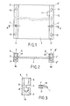
- a plate holder according to the invention is shown in plan view.
- a plate for example a Teflon or polyether sulfone plate laminated with copper on both sides and provided with conductor tracks, is arranged between two elongated and rod-shaped frame parts 2 and 2 'and inserted with the opposite edges into corresponding grooves 3 and 3', the depth of which is shown by the dashed lines is indicated within the frame parts 2, 2 '.
- Soldering channels 4 and 4 ' run from the top of the frame parts 2, 2' to the grooves 3, 3 'underneath and thereby connect them to the outside space.
- various types of fastening holes 14 can be provided in the frame parts 2, 2', which, in the form of continuous bores or threaded holes, serve to connect the frame parts 2, 2 'to a base and / or cover plates. Furthermore, it is possible to leave recesses 11 on the edge of the plate, which in connection with a corresponding through-bore 15 through the frame part 2 'has space for externally operable circuit elements, e.g. Trimmer, or power supply through feedthrough capacitors.
- circuit elements e.g. Trimmer
- FIG. 2 shows the cross section through a plate holder according to FIG. 1 in a plane identified by the line AA 'in FIG. 1.
- the frame parts 2, 2 typically have a prismatic cross section.
- the grooves 3, 3 ' run in the longitudinal direction on the frame inner sides 5, 5' and have a depth of several millimeters, which is sufficient on the one hand to give the plate 1 sufficient support and on the other hand does not take up an unnecessarily large area from the plate 1 takes. If the plate is a double sided printed.
- Printed circuit board is, which is equipped from the top and bottom with electronic components of a certain height, it is expedient that the grooves 3 and 3 'run in the central region of the frame inner sides 5, 5' to complete on both sides of the board Shielding housing to gain enough space.
- solder channels 4, 4 ' extend at least to the grooves 3, 3' from the frame tops 6, 6 ', but are closed towards the frame undersides 16 and 16', so that the liquid solder from the solder channels 4, 4 during the soldering process 'into the groove 3, 3', but cannot flow out downwards.
- the solder channels 4, 4' it is advantageous to design the solder channels 4, 4' as vertical blind holes to the plate 1, which extend through the groove 3, 3 'in depth if the soldering is to be carried out on both sides, and with them Central axes are arranged with respect to the groove depth such that they are only partially cut by the grooves. Such blind holes are very easy to make using automatic drills.
- a recess 11 at the edge of the plate, as shown in FIG. 1.
- a trimmer can be arranged lying, which is connected to the circuit by conductor tracks on the plate 1 is. Since such a recess 11 interrupts the continuous soldering of the plate edge 12 ', in this case 11 solder channels must be provided on both sides of the recess in order to supply the solder required for the soldering process on both sides.
- the frame parts 2, 2' have a surface which has excellent solderability with excellent electrical conductivity combined. This is achieved very advantageously and at the same time economically in that the frame parts are made of an inexpensive metal, e.g. Brass, are made and have a silver-plated surface.
- the soldered connection is then expediently imparted by a solder saturated with silver, which prevents silver from dissolving from the surface layer of the frame parts during the soldering process and impairing the quality of the soldered joint.
- the distribution of the liquid solder from the soldering channels 4, 4 'into the gap-shaped spaces formed on both sides of the plate edges between the grooves 3, 3' and the plate edges 12, 12 ' takes place by capillary forces and is therefore closely related to the geometric dimensions of the latter Spaces together. So that the capillary forces are effective but also the amount of solder required is kept low, it is advantageous that the width of the grooves 3, 3 'only exceeds the thickness of the plate edges 12, 12' in them by less than 0.2 mm. For example, if the thickness is 1.6 mm, excellent results with regard to the soldered connection are obtained with a groove width of 1.7 mm.
- the flow properties of the solder used and the geometric dimensions of frame parts 2, 2 ' and plate 1 determines the appropriate distribution of the various solder channels along the frame parts. If the solder from a solder channel penetrates only a few millimeters sideways into the gap between the frame part and the edge of the plate, the solder channels must be arranged in a correspondingly denser sequence than if the maximum propagation path is several centimeters. In the case of frame parts with a silver-plated surface and a groove depth of approximately 2.5 mm and when using a conventional soft solder, distances between adjacent solder channels of 10-30 mm have proven effective.
- Fig. 3 the cross section through a frame part 2 and the edge part of the plate 1 is shown on an enlarged scale before assembly.
- the groove inner surfaces 8 and 8 'are used which are opposite edge surfaces 7 and 7' in the inserted state.
- these edge surfaces 7, 7 'are copper layers with a width that is at least approximately as large as the groove depth and a surface that pretreated to improve the solderability, e.g. can be pre-tinned. It is particularly advantageous if the edge surfaces 7, 7 'are somewhat wider than the groove depth, because after the soldering process the quality of the soldering can then be checked optically using the visible soldering strip.
- the shielding of the circuit is completed in the manner shown in FIG. 4.
- the shielding housing is closed at the top and bottom by electrically conductive cover plates 9 and 9 ', which bear against the frame parts 2 and 2' with good electrical contact and are fastened to them.
- the lower cover plate 9 ' can also are replaced by the fact that the frame parts 2 and 2 ', with the soldered plate 1 in between, are scraped onto a larger, conductive carrier plate which takes over the lower part of the shield and also carries other plate holders of the same type.
- the transverse sides can be covered together with the open upper side if an upper cover plate 9 with angled and adapted side surfaces is used.
- the solder is filled into the soldering channels 4, 4'. This can be done in such a way that pieces of a solder wire of the required length and with a diameter not much smaller than that of the solder channel are inserted into the solder channel. When heated, the molten solder then fills the solder channel and spreads sideways along the groove from the solder channel.
- the frame parts are heated until the solder melts in the solder channels and flows into the groove. So that the flow process is not impaired by a very different temperature distribution in the frame parts 2, 2 ', the heating should take place as uniformly as possible over the entire length of the frame. This can be achieved with a soldering arrangement as shown in FIG. 5.
- the frame parts 2, 2 'with the inserted plate 1 are placed on a highly heat-conductive and dimensionally stable, flat base 19, which is heated from its underside with the necessary heat H and, due to its good thermal conductivity, distributes the temperature evenly.
- a plate holder according to the invention proves to be a mechanically stable and electrically reliable arrangement for a printed circuit board, which on the one hand requires a good earth connection and on the other hand has to be adequately shielded.
- a particular advantage of the holder is that it can be produced automatically in a simple manner.
Abstract
Description
Die Erfindung geht aus von einer Plattenhalterung, insbesondere für RF-Leiterplatten, gemäss dem Oberbegriff des Anspruchs 1.The invention is based on a plate holder, in particular for RF printed circuit boards, according to the preamble of
Eine solche Plattenhalterung wird seit langem in elektronischen Geräten verwendet, in denen bestimmte Schaltungsteile, zu Baugruppen zusammengefasst, auf einer Anzahl von Leiterplatten mit gedruckten Schaltungen untergebracht und auswechselbar gehaltert werden. Die Rahmenteile, die üblicherweise aus einem isolierenden Kunststoff hergestellt sind, weisen in ihrer Längsrichtung Nute auf, die in einer Weise auf die Abmessungen der Leiterplatte abgestimmt sind, dass die Platte ohne Schwierigkeiten von der Vorderseite her eingeschoben und auch wieder herausgezogen werden kann. Quer zur Nutrichtung sind am hinteren Ende der Rahmenteile häufig Steckerleisten angebracht, in die entsprechende Vorrichtungen auf der Leiterplatte beim Einschieben automatisch eingesteckt werden und die erforderlichen elektrischen Verbindungen zu anderen Schaltungsteilen herstellen.Such a plate holder has long been used in electronic devices in which certain circuit parts, combined into assemblies, are accommodated on a number of printed circuit boards with printed circuits and are held interchangeably. The frame parts, which are usually made of an insulating plastic, have grooves in their longitudinal direction which are matched to the dimensions of the printed circuit board in such a way that the board can be pushed in and pulled out again from the front without difficulty. At the rear end of the frame parts, connector strips are often attached at right angles to the groove direction, into which corresponding devices on the printed circuit board are automatically inserted when they are inserted and establish the necessary electrical connections to other circuit parts.
Während die beschriebenen Rahmenteile lediglich mechanisch wirkende Halterungen ohne eine elektrische Aufgabe darstellen, ist es im Falle von äusserst störempfindlichen oder beispielsweise Hochfrequenz-Schaltungen oftmals unerlässlich, die Leiterplatten in einem abschirmenden Metallgehäuse unterzubringen, das mit der Masseleitung der Schaltung gut leitend verbunden ist, und die Haltevorrichtungen in geeigneter Weise zu modifizieren. Insbesondere ist es jedoch bei sehr hohen Betriebsfrequenzen im GHz-Bereich zunehmend wichtig, die Gehäusegeometrie so auszulegen, dass sich im Zusammenwirken mit der Leiterplatte und ihrer Schaltung die erwünschten Hochfrequenzeigenschaften ergeben. Dies führt zum Aufbau weitgehend vorgefertigter, häufig gefräster oder aus Blechen gebogener und zusammengelöteter Gehäuse, in welche die Leiterplatten nachträglich eingesetzt und dann befestigt werden.While the described frame parts only represent mechanically acting brackets without an electrical task, in the case of extremely interference-sensitive or, for example, high-frequency circuits, it is often essential to accommodate the printed circuit boards in a shielding metal housing, which is well conductively connected to the ground line of the circuit, and that Modify holding devices in a suitable manner. In particular, however, at very high operating frequencies in the GHz range, it is increasingly important to design the housing geometry in such a way that the desired high-frequency properties result in interaction with the printed circuit board and its circuit. This leads to the construction of largely prefabricated, often milled or bent and made of sheet metal and soldered housings, in which the circuit boards are subsequently inserted and then attached.
Diese Art des Gehäuseaufbaus ist einerseits in der Fertigung sehr aufwendig. Auf der anderen Seite bereitet es aber auch Probleme, im Anschluss an den Einbau der Platte einen elektrisch zuverlässigen, grossflächigen Massekontakt zwischen der Schaltung und der Abschirmung herzustellen.On the one hand, this type of housing construction is very complex to manufacture. On the other hand, it is also problematic to establish an electrically reliable, large-area ground contact between the circuit and the shield after the plate has been installed.
Der vorliegenden Erfindung liegt daher die Aufgabe zugrunde, eine Plattenhalterung zu schaffen, die gleichermassen den einfachen Aufbau einer vollständigen Abschirmung ermöglicht, eine sehr gute und beständige elektrische sowie mechanische Verbindung zwischen Schaltung und Abschirmgehäuse herzustellen gestattet und ohne grossen Aufwand realisiert werden kann.The present invention is therefore based on the object of providing a plate holder which likewise enables the simple construction of a complete shield, allows a very good and stable electrical and mechanical connection between the circuit and the shielding housing, and can be implemented without great effort.
Die Aufgabe wird bei einer Plattenhalterung der eingangs genannten Art durch die Merkmale aus dem kennzeichnenden Teil des Anspruchs 1 gelöst.The object is achieved in a plate holder of the type mentioned by the features from the characterizing part of
Die erfindungsgemässe Plattenhalterung hat den Vorteil, dass sie eine mechanisch und elektrisch sichere Verbindung zwischen der Platte und den Rahmenteilen aufweist, durch entsprechende obere und untere Abdeckplatte ohne Probleme zu einem hochfrequenzdichten Abschirmgehäuse erweitert werden kann und mit Hilfe der Lötkanäle in einfacher und für eine automatisierte Fertigung geeigneter Weise hergestellt werden kann.The plate holder according to the invention has the advantage that it has a mechanically and electrically secure connection has between the plate and the frame parts, can be expanded without problems to a high-frequency-tight shielding housing by means of corresponding upper and lower cover plates and can be produced with the aid of the soldering channels in a simple manner suitable for automated production.
Bei dem Verfahren zur Herstellung der erfindungsgemässen Plattenhalterung wird die Platte mit ihren Rändern zunächst in die Nute der mit den Lötkanälen versehenen Rahmenteile eingeschoben. Dann wird ein geeignetes Lot von oben in die Lötkanäle eingefüllt. Danach werden die Rahmenteile auf eine Temperatur oberhalb der Schmelztemperatur des verwendeten Lotes erhitzt und solange oberhalb der Schmelztemperatur gehalten, bis das nun flüssige Lot aus den Lötkanälen beidseitig zwischen die Plattenränder und die Nutinnenflächen geflossen ist und sich dort verteilt hat. Schliesslich wird durch Abkühlen eine feste Lötverbindung zwischen der Platte und den Rahmenteilen hergestellt.In the method for producing the plate holder according to the invention, the edges of the plate are first inserted into the groove of the frame parts provided with the solder channels. A suitable solder is then filled into the soldering channels from above. The frame parts are then heated to a temperature above the melting temperature of the solder used and kept above the melting temperature until the now liquid solder has flowed from the soldering channels on both sides between the plate edges and the inner surfaces of the groove and has been distributed there. Finally, a firm solder connection between the plate and the frame parts is made by cooling.
Nachfolgend soll nun die Erfindung in Ausführungsbeispielen anhand der Zeichnung beschrieben und näher erläutert werden. Es zeigen:
- Fig. 1 eine Plattenhalterung nach der Erfindung in Draufsicht,
- Fig. 2 den Querschnitt durch eine Plattenhalterung nach Fig. 1 in der mit A-A bezeichneten Ebene aus Fig. 1,
- Fig. 3 den vergrösserten Querschnitt durch ein Rahmenteil und den zugeordneten Plattenrand vor dem Einschieben der Platte in die Nut,
- Fig. 4 eine mit Abdeckplatten komplettierte Plattenhalterung mit einer innenliegenden und abgeschirmten, elektronischen Schaltung, und
- Fig. 5 im Querschnitt eine bevorzugte Anordnung zum Herstellen der Lötverbindung.
- 1 is a top view of a plate holder according to the invention,
- 2 shows the cross section through a plate holder according to FIG. 1 in the plane designated by AA from FIG. 1,
- 3 shows the enlarged cross section through a frame part and the associated plate edge before the plate is inserted into the groove,
- Fig. 4 is a plate holder completed with cover plates tion with an internal and shielded electronic circuit, and
- Fig. 5 in cross section a preferred arrangement for making the solder joint.
In Fig. 1 ist eine erfindungsgemässe Plattenhalterung in der Draufsicht dargestellt. Eine Platte 1, beispielsweise eine beidseitig mit Kupfer kaschierte und mit Leiterbahnen versehene Teflon- oder Polyäthersulfonplatte ist zwischen zwei länglichen und stabförmigen Rahmenteilen 2 und 2' angeordnet und mit den gegenüberliegenden Rändern in entsprechende Nute 3 und 3' eingeschoben, deren Tiefe durch die gestrichelten Linien innerhalb der Rahmenteile 2, 2' angedeutet ist. Von der Oberseite der Rahmenteile 2, 2' her verlaufen Lötkanäle 4 und 4' zu den darunterliegenden Nuten 3, 3' hin und verbinden diese dadurch mit dem Aussenraum. Weiterhin können neben diesen Lötkanälen 4, 4' verschiedenartige Befestigungslöcher 14 in den Rahmenteilen 2, 2' vorgesehen werden, die in Form durchgehender Bohrungen oder Gewindelöcher dazu dienen, die Rahmenteile 2, 2' mit einer Unterlage und/oder Abdeckplatten zu verbinden. Weiterhin ist es möglich, am Rand der Platte Aussparungen 11 freizulassen, die in Verbindung mit einer entsprechenden Durchgangsbohrung 15 durch das Rahmenteil 2' Raum für von aussen bedienbare Schaltungselemente, z.B. Trimmer, oder Stromzuführungen über Durchführungskondensatoren geben.In Fig. 1, a plate holder according to the invention is shown in plan view. A
Fig. 2 zeigt den Querschnitt durch eine Plattenhalterung nach Fig. l in einer durch die Linie A-A' in Fig. 1 gekennzeichnete Ebene. Die Rahmenteile 2, 2' haben typischerweise einen prismatischen Querschnitt. Die Nute 3, 3' verlaufen in Längsrichtung auf den Rahmeninnenseiten 5, 5' und haben eine Tiefe von mehreren Millimetern, die einerseits ausreicht, um der Platte 1 genügend Halt zu geben, und andererseits nicht eine unnötig grosse Fläche von der Platte 1 in Anspruch nimmt. Wenn die Platte l eine doppelseitig bedruckte. Leiterplatte ist,.die von der Ober- und Unterseite her mit elektronischen Bauelementen einer gewissen Bauhöhe bestückt wird, ist es zweckmässig, dass die Nute 3 und 3' im Mittelbereich der Rahmeninnenseiten 5, 5' verlaufen, um auf beiden Seiten der Platte im komplettierten Abschirmgehäuse ausreichend Platz zu gewinnen.FIG. 2 shows the cross section through a plate holder according to FIG. 1 in a plane identified by the line AA 'in FIG. 1. The
Von den Rahmenoberseiten 6, 6' her reichen die Lötkanäle 4, 4' wenigstens bis zu den Nuten 3, 3', sind aber zu den Rahmenunterseiten 16 und 16' hin geschlossen, damit beim Lötvorgang das flüssige Lot zwar aus den Lötkanälen 4, 4' in die Nute 3, 3' hinein, nicht jedoch nach unten herausfliessen kann. Für eine Serienfertigung der Rahmenteile 2, 2' ist es vorteilhaft, die Lötkanäle 4, 4' als zur Platte 1 senkrechte Sacklöcher auszuführen, die in ihrer Tiefe durch die Nute 3, 3' hindurchreichen, wenn die Lötung beidseitig erfolgen soll, und mit ihren Mittelachsen bezüglich der Nuttiefe dergestalt angeordnet sind, dass sie von den Nuten lediglich teilweise angeschnitten werden. Solche Sacklöcher sind mittels Bohrautomaten sehr einfach herzustellen. Insbesondere wird aber durch ihre Anordnung erreicht, dass das in den Lötkanälen 4, 4' befindliche, aufgeschmolzene Löt während des Lötvorganges ungehindert um die Plattenkanten herum die Plattenränder 12, 12' in den Nuten 3, 3' von beiden Seiten benetzen kann. Auf diese Weise kann in einem Arbeitsgang die beidseitige Lötung zwischen der Platte 1 und den Rahmenteilen 2, 2' durchgeführt werden. Die Lötung erstreckt sich dabei üblicherweise über die gesamte Länge der Rahmenteile 2, 2', um so einen geschlossenen mechanischen und elektrischen Uebergang zwischen ihnen und der Platte 1 zu ermöglichen.The
In bestimmten Fällen ist es jedoch vorteilhaft, eine Aussparung 11 am Rand der Platte vorzusehen, wie sie in Fig. l eingezeichnet ist. In dieser Aussparung 11 kann beispielsweise liegend ein Trimmer angeordnet werden, der durch Leiterbahnen auf der Platte 1 mit der Schaltung verbunden ist. Da eine solche Aussparung 11 die durchgehende Verlötung des Plattenrandes 12' unterbricht, müssen in diesem Fall auf beiden Seiten der Aussparung 11 Lötkanäle vorgesehen werden, um auf beiden Seiten das für den Lötvorgang erforderliche Lot zuzuführen.In certain cases, however, it is advantageous to provide a
Für die Qualität der Lötung und insbesondere für gute HF- bzw. Abschirmeigenschaften der Rahmenteile 2, 2' und der mit ihnen verbundenen Abdeckplatten ist es wünschenswert, wenn die Rahmenteile 2, 2' eine Oberfläche besitzen, die eine hervorragende Lötfähigkeit mit einer ausgezeichneten elektrischen Leitfähigkeit kombiniert. Dies wird sehr vorteilhaft und zugleich wirtschaftlich dadurch erreicht, dass die Rahmenteile massiv aus einem preisgünstigen Metall, z.B. Messing, gefertigt sind und eine versilberte Oberfläche aufweisen. Gleichzeitig wird dann auch zweckmässigerweise die Lötverbindung durch ein mit Silber gesättigtes Lot vermittelt, wodurch verhindert wird, dass während des Lötvorganges Silber aus der Oberflächenschicht der Rahmenteile in Lösung geht und die Qualität der Lötstelle beeinträchtigt.For the quality of the soldering and in particular for good HF or shielding properties of the
Die Verteilung des flüssigen Lotes aus den Lötkanälen 4, 4' in die zwischen den Nuten 3, 3' und den Plattenrändern 12, 12' gebildeten, spaltförmigen Räume auf beiden Seiten der Plattenränder erfolgt durch kapillare Kräfte und hängt daher eng mit den geometrischen Abmessungen dieser Räume zusammen. Damit die Kapillarkräfte wirksam werden aber auch die Menge des benötigten Lotes gering gehalten wird, ist es vorteilhaft, dass die Breite der Nute 3, 3' die Dicke der in ihnen liegenden Plattenränder 12, 12' nur um weniger als 0,2 mm übersteigt. Beträgt die Dicke also beispielsweise 1,6 mm, so werden mit einer Nutbreite von 1,7 mm ausgezeichnete Ergebnisse im Bezug auf die Lötverbindung erhalten. Je nach der Vorbehandlung der zu lötenden Flächen, den Fliesseigenschaften des verwendeten Lotes und der geometrischen Abmessungen von Rahmenteilen 2, 2' und Platte 1 richtet sich die geeignete Verteilung der verschiedenen Lötkanäle entlang der Rahmenteile. Dringt das Lot aus einem Lötkanal nur wenige Millimeter seitwärts in die Spalte zwischen Rahmenteil und Plattenrand vor, müssen die Lötkanäle in einer entsprechend dichteren Abfolge vorgesehen werden, als wenn der maximale Ausbreitungsweg mehrere Zentimeter beträgt. Bei Rahmenteilen mit versilberter Oberfläche und einer Nuttiefe von etwa 2,5 mm und bei Verwendung eines üblichen Weichlots haben sich Abstände zwischen benachbarten Lötkanälen von 10-30 mm bewährt.The distribution of the liquid solder from the
In Fig. 3 ist in vergrössertem Massstab der Querschnitt durch ein Rahmenteil 2 und den Randteil der Platte 1 vor dem Zusammenbau dargestellt. Für die Lötung werden die Nutinnenflächen 8 und 8' benutzt, denen im eingeschobenen Zustand Randoberflächen 7 und 7' gegenüberliegen. Im Falle einer üblichen Leiterplatte handelt es sich bei diesen Randoberflächen 7, 7' um Kupferschichten mit einer Breite, die wenigstens annähernd so gross wie die Nuttiefe ist und einer Oberfläche, die zur.Verbesserung der Lötfähigkeit vorbehandelt, also z.B. vorverzinnt sein kann. Besonders vorteilhaft ist es, wenn die Randoberflächen 7, 7' etwas breiter als die Nuttiefe sind, weil dann nach dem Lötvorgang die Qualität der Lötung anhand des sichtbaren Lötstreifens optisch kontrolliert werden kann. Die Randoberflächen 7, 7' sind ein Teil des auf die Platte gedruckten Leitungssystems und stellen die elektrische Verbindung zwischen der Schaltung und dem Rahmenteil 2 her.In Fig. 3, the cross section through a
Die Abschirmung der Schaltung wird nach der in Fig. 4 gezeigten Art vervollständigt. Nach oben und unten wird das Abschirmgehäuse durch elektrisch leitende Abdeckplatten 9 und 9' abgeschlossen, die an den Rahmenteilen 2 und 2' mit gutem elektrischen Kontakt anliegen und an ihnen befestigt sind. Die untere Abdeckplatte 9' kann aber auch dadurch ersetzt werden, dass die Rahmenteile 2 und 2', mit der verlöteten Platte 1 dazwischen, auf eine grössere, leitende Trägerplatte aufgeschruabt sind, die den unteren Teil der Abschirmung übernimmt und daneben noch andere Plattenhalterungen der gleichen Art trägt. Die Querseiten lassen sich zusammen mit der offenen Oberseite abdecken, wenn eine obere Abdeckplatte 9 mit abgewinkelten und angepassten Seitenflächen verwendet wird.The shielding of the circuit is completed in the manner shown in FIG. 4. The shielding housing is closed at the top and bottom by electrically
Die in Fig. 4 dargestellte Anordnung von drei parallelen Platten 9, 1 und 9', von denen die mittlere Platte 1 eine Schaltung mit elektronischen Bauelementen 13 und gegebenfalls von aussen bedienbare Trimmer 17 trägt, bildet zwei Hohlräume 10 und 10', die sich vorteilhaft zum Aufbau von Schaltungselementen, insbesondere Induktivitäten und Kapazitäten für Höchstfrequenz-Anwendungen im GHz-Bereich einsetzen lassen. Durch entsprechend gestaltete Leiterflächen auf beiden Seiten der Platte 1, die den leitenden Abdeckplatten gegenüberliegen, können z.B. zusammen mit den Abdeckplatten Resonanzelemente aufgebaut werden, die aufgrund des festen mechanischen Aufbaus der Plattenhalterung in ihrer Geometrie festliegen und reproduzierbare elektrische Eigenschaften besitzen.The arrangement of three
Bei der Herstellung der Plattenhalterung wird nach dem Einschieben der normalerweise unbestückten Platte 1 mit ihren Plattenrändern 12 und 12' in die Nute 3, 3' der Rahmenteile 2 und 2' das Lot in die Lötkanäle 4, 4' eingefüllt. Dies kann in einer Weise geschehen, dass Stücke eines Lötdrahtes in der erforderlichen Länge und mit einem Durchmesser nicht viel kleiner als der des Lötkanals, in den Lötkanal eingeführt werden. Beim Erhitzen erfüllt dann das geschmolzene Lot den Lötkanal und breitet sich längs der Nute vom Lötkanal her seitwärts aus. Um die Benetzung der Nutinnenflächen 8 und 8' durch das Lot zu verbessern, ist es vorteilhaft, die Nute 3, 3' vorher mit einem zum verwendeten Lot passenden Flussmittel zu behandeln, wie dies dem Fachmann an sich bekannt ist. Für die automatisierte Fertigung besonders günstig ist es aber auch, das Lot zusammen mit einem Flussmittel in Form einer fein vermischten, cremeartigen Lötpaste einzufüllen. Eine solche Paste lässt sich mittels einer Dosie.r-maschine in genau der erforderlichen Menge in die Lötkanäle eingeben, wobei die feine Verteilung des Flussmittels das Fliessen und Benetzen des Lotes in den schmalen Spalten zwischen Rahmenteil und Plattenrand fördert. Gute Ergebnisse wurden mit einem niedrigschmelzenden Lot erzielt, das eine Schmelztemperatur von ungefähr 180°C hatte.In the manufacture of the plate holder, after inserting the normally
Nachdem das Lot in die Lötkanäle eingefüllt ist, werden die Rahmenteile soweit erhitzt, bis das Lot in den Lötkanälen schmilzt und in die Nute einfliesst. Damit der Fliessvorgang nicht durch eine stark unterschiedliche Temperaturverteilung in den Rahmenteilen 2, 2' beeinträchtigt wird, sollte die Erwärmung möglichst gleichmässig über die gesamte Rahmenlänge erfolgen. Dies kann mit einer Lötanordnung erreicht werden, wie sie in Fig. 5 wiedergegeben ist. Die Rahmenteile 2, 2' mit der eingeschobenen Platte 1 werden auf eine gut wärmeleitende und unter Wärmeeinwirkung formbeständige, ebene Unterlage 19 gebracht, die von ihrer Unterseite her mit der nötigen Hitze H geheizt wird und aufgrund ihrer guten Wärmeleitfähigkeit die Temperatur gleichmässig verteilt. Zusätzlich ist es von Vorteil, die Platte 1 mit einer wärmebeständigen und wärmeisolierenden Zwischenlage 18, die zwischen Platte 1 und Unterlage 19 angeordnet ist, vor der Wärmestrahlung und -konvektion der Unterlage 19 zu schützen. Für die automatische Fertigung ist es auch günstig, wenn die Rahmenteile 2 und 2' für den Lötvorgang durch einen im wesentlichen parallel zu den Nuten 3, 3' fliessenden, starken Strom erhitzt werden, der mittels an den Enden angebrachter, elektrischer Kontakte durch die Rahmenteile geleitet wird.After the solder has been filled into the solder channels, the frame parts are heated until the solder melts in the solder channels and flows into the groove. So that the flow process is not impaired by a very different temperature distribution in the
Insgesamt erweist sich eine Plattenhalterung gemäss der Erfindung als eine mechanisch stabile und elektrisch zuverlässige Anordnung für eine Leiterplatte, die einerseits eine gute Masseverbindung benötigt und andererseits ausreichend abgeschirmt werden muss. Ein besonderer Vorteil der Halterung liegt darin, dass ihre Herstellung in einfacher Weise automatisch erfolgen kann.Overall, a plate holder according to the invention proves to be a mechanically stable and electrically reliable arrangement for a printed circuit board, which on the one hand requires a good earth connection and on the other hand has to be adequately shielded. A particular advantage of the holder is that it can be produced automatically in a simple manner.
Claims (10)
Priority Applications (1)
| Application Number | Priority Date | Filing Date | Title |
|---|---|---|---|
| AT84102492T ATE25913T1 (en) | 1983-03-25 | 1984-03-08 | PLATE HOLDER, PARTICULARLY FOR RF CIRCUIT BOARDS, AND A METHOD OF PRODUCTION THEREOF. |
Applications Claiming Priority (2)
| Application Number | Priority Date | Filing Date | Title |
|---|---|---|---|
| CH1649/83 | 1983-03-25 | ||
| CH164983 | 1983-03-25 |
Publications (2)
| Publication Number | Publication Date |
|---|---|
| EP0124712A1 true EP0124712A1 (en) | 1984-11-14 |
| EP0124712B1 EP0124712B1 (en) | 1987-03-11 |
Family
ID=4215391
Family Applications (1)
| Application Number | Title | Priority Date | Filing Date |
|---|---|---|---|
| EP84102492A Expired EP0124712B1 (en) | 1983-03-25 | 1984-03-08 | Board fixture, especially for a circuit board, and method for its manufacture |
Country Status (5)
| Country | Link |
|---|---|
| US (1) | US4609970A (en) |
| EP (1) | EP0124712B1 (en) |
| AT (1) | ATE25913T1 (en) |
| DE (1) | DE3462652D1 (en) |
| NO (1) | NO161770C (en) |
Cited By (3)
| Publication number | Priority date | Publication date | Assignee | Title |
|---|---|---|---|---|
| EP0278382A2 (en) * | 1987-02-06 | 1988-08-17 | Siemens Aktiengesellschaft Österreich | Barrier filter |
| EP0381378A2 (en) * | 1989-02-03 | 1990-08-08 | Nokia Mobile Phones Ltd. | Method for manufacturing the chassis of a radio telephone and a chassis manufactured according to said method |
| EP0608718A2 (en) * | 1993-01-27 | 1994-08-03 | Siemens Nixdorf Informationssysteme Aktiengesellschaft | Device for reducing stray radiation from flat assemblies |
Families Citing this family (6)
| Publication number | Priority date | Publication date | Assignee | Title |
|---|---|---|---|---|
| US5244840A (en) * | 1989-05-23 | 1993-09-14 | Mitsubishi Denki Kabushiki Kaisha | Method for manufacturing an encapsulated IC card having a molded frame and a circuit board |
| SE468575B (en) * | 1991-06-14 | 1993-02-08 | Ericsson Telefon Ab L M | DEVICE WITH LAMINATING CONDUCTING PATTERNS AND SELECTIVE DIELECTRICS |
| US5285353A (en) * | 1992-12-28 | 1994-02-08 | Delco Electronics Corporation | Support bar for circuit boards |
| FI119756B (en) * | 1995-01-18 | 2009-03-13 | Alteon Inc | Use of Thiazolium Compounds to Prevent and Reverse Formation of Long-End Glycosylation |
| US20050014747A1 (en) * | 2003-04-18 | 2005-01-20 | Emily Reinhard | Dihydrothiazine prodrugs of thiazolium agents |
| JP6683670B2 (en) * | 2017-11-21 | 2020-04-22 | ファナック株式会社 | Lock mechanism |
Citations (4)
| Publication number | Priority date | Publication date | Assignee | Title |
|---|---|---|---|---|
| CH379211A (en) * | 1960-09-01 | 1964-06-30 | Sulzer Ag | Connection of two cylindrical metallic workpieces by gap soldering |
| GB1073108A (en) * | 1965-02-16 | 1967-06-21 | Siemens Ag | Improvements in or relating to the screening of printed circuit boards |
| FR2116630A5 (en) * | 1970-12-01 | 1972-07-21 | Cit Alcatel | |
| GB2029645A (en) * | 1978-08-07 | 1980-03-19 | Mitsumi Electric Co Ltd | High-frequency circuit device |
Family Cites Families (4)
| Publication number | Priority date | Publication date | Assignee | Title |
|---|---|---|---|---|
| US3806767A (en) * | 1973-03-15 | 1974-04-23 | Tek Wave Inc | Interboard connector |
| FR2246154A1 (en) * | 1974-06-06 | 1975-04-25 | Precitec Gmbh | Grips for printed circuit boards - which can easily and rapidly be installed use sharp edged clips to dig into board |
| US3992653A (en) * | 1975-08-18 | 1976-11-16 | Sperry Rand Corporation | Zero insertion force card guide |
| US4517625A (en) * | 1983-11-09 | 1985-05-14 | Lockheed Corporation | Circuit board housing with zero insertion force connector |
-
1984
- 1984-03-08 EP EP84102492A patent/EP0124712B1/en not_active Expired
- 1984-03-08 AT AT84102492T patent/ATE25913T1/en not_active IP Right Cessation
- 1984-03-08 DE DE8484102492T patent/DE3462652D1/en not_active Expired
- 1984-03-16 NO NO841047A patent/NO161770C/en unknown
- 1984-03-22 US US06/592,279 patent/US4609970A/en not_active Expired - Fee Related
Patent Citations (4)
| Publication number | Priority date | Publication date | Assignee | Title |
|---|---|---|---|---|
| CH379211A (en) * | 1960-09-01 | 1964-06-30 | Sulzer Ag | Connection of two cylindrical metallic workpieces by gap soldering |
| GB1073108A (en) * | 1965-02-16 | 1967-06-21 | Siemens Ag | Improvements in or relating to the screening of printed circuit boards |
| FR2116630A5 (en) * | 1970-12-01 | 1972-07-21 | Cit Alcatel | |
| GB2029645A (en) * | 1978-08-07 | 1980-03-19 | Mitsumi Electric Co Ltd | High-frequency circuit device |
Cited By (6)
| Publication number | Priority date | Publication date | Assignee | Title |
|---|---|---|---|---|
| EP0278382A2 (en) * | 1987-02-06 | 1988-08-17 | Siemens Aktiengesellschaft Österreich | Barrier filter |
| EP0278382A3 (en) * | 1987-02-06 | 1989-10-18 | Siemens Aktiengesellschaft Österreich | Barrier filter |
| EP0381378A2 (en) * | 1989-02-03 | 1990-08-08 | Nokia Mobile Phones Ltd. | Method for manufacturing the chassis of a radio telephone and a chassis manufactured according to said method |
| EP0381378A3 (en) * | 1989-02-03 | 1992-01-08 | Nokia Mobile Phones Ltd. | Method for manufacturing the chassis of a radio telephone and a chassis manufactured according to said method |
| EP0608718A2 (en) * | 1993-01-27 | 1994-08-03 | Siemens Nixdorf Informationssysteme Aktiengesellschaft | Device for reducing stray radiation from flat assemblies |
| EP0608718A3 (en) * | 1993-01-27 | 1996-01-10 | Siemens Nixdorf Inf Syst | Device for reducing stray radiation from flat assemblies. |
Also Published As
| Publication number | Publication date |
|---|---|
| ATE25913T1 (en) | 1987-03-15 |
| EP0124712B1 (en) | 1987-03-11 |
| US4609970A (en) | 1986-09-02 |
| NO161770B (en) | 1989-06-12 |
| NO841047L (en) | 1984-09-26 |
| DE3462652D1 (en) | 1987-04-16 |
| NO161770C (en) | 1989-09-20 |
Similar Documents
| Publication | Publication Date | Title |
|---|---|---|
| EP0920055B1 (en) | Cooling device for a heat generating component on a printed board | |
| DE3790315C2 (en) | ||
| DE2532670C2 (en) | ||
| DE4020498C2 (en) | Method for producing multiwire printed circuit boards with insulated metal conductors and / or optical conductors | |
| DE19634202C2 (en) | Semiconductor device | |
| DE4203605A1 (en) | ELECTRIC CONNECTOR | |
| DE10111718A1 (en) | Electronic circuit device has one board connected by solder to metal spacers, which are connected to other board by conductive adhesive | |
| DE3535923A1 (en) | SUBSTRATE CONSTRUCTION | |
| DE2103064A1 (en) | Device for the production of modular elements | |
| EP0124712B1 (en) | Board fixture, especially for a circuit board, and method for its manufacture | |
| DE2639979B2 (en) | Semiconductor module | |
| DE69838604T2 (en) | PRINTED PLATE AND METHOD FOR THE PRODUCTION THEREOF | |
| DE3525012A1 (en) | BUS BAR FOR SURFACE MOUNTING | |
| DE3902998C2 (en) | ||
| DE3731413A1 (en) | Electrical switching apparatus | |
| DE10064221B4 (en) | Printed circuit board with cooled SMD component | |
| DE3323830C2 (en) | Arrangement for soldering an electrical circuit board onto a base body | |
| EP0166817B1 (en) | Method and device for soldering leads of electric components as well as arrangement of electric components | |
| DE1059988B (en) | Electrical assembly | |
| DE1927387A1 (en) | Solar battery | |
| EP0204379B1 (en) | Production method for an air-tight component enclosure, in particular for a quartz resonator | |
| EP0651598B1 (en) | Electronic circuit module | |
| DE4008658C2 (en) | ||
| DE102011090002A1 (en) | Printed circuit board of printed circuit board assembly used in automotive industry, has patterned metallization layer set facing away from cover layer, and metal core structure consisting of conductor track partially exposed by recess | |
| DE19826023C2 (en) | Multi-layer electrical circuit arrangement |
Legal Events
| Date | Code | Title | Description |
|---|---|---|---|
| PUAI | Public reference made under article 153(3) epc to a published international application that has entered the european phase |
Free format text: ORIGINAL CODE: 0009012 |
|
| AK | Designated contracting states |
Designated state(s): AT CH DE GB LI |
|
| 17P | Request for examination filed |
Effective date: 19840914 |
|
| GRAA | (expected) grant |
Free format text: ORIGINAL CODE: 0009210 |
|
| AK | Designated contracting states |
Kind code of ref document: B1 Designated state(s): AT CH DE GB LI |
|
| REF | Corresponds to: |
Ref document number: 25913 Country of ref document: AT Date of ref document: 19870315 Kind code of ref document: T |
|
| REF | Corresponds to: |
Ref document number: 3462652 Country of ref document: DE Date of ref document: 19870416 |
|
| RAP2 | Party data changed (patent owner data changed or rights of a patent transferred) |
Owner name: BBC BROWN BOVERI AG |
|
| PLBE | No opposition filed within time limit |
Free format text: ORIGINAL CODE: 0009261 |
|
| STAA | Information on the status of an ep patent application or granted ep patent |
Free format text: STATUS: NO OPPOSITION FILED WITHIN TIME LIMIT |
|
| 26N | No opposition filed | ||
| PGFP | Annual fee paid to national office [announced via postgrant information from national office to epo] |
Ref country code: GB Payment date: 19890228 Year of fee payment: 6 |
|
| PGFP | Annual fee paid to national office [announced via postgrant information from national office to epo] |
Ref country code: AT Payment date: 19890302 Year of fee payment: 6 |
|
| PGFP | Annual fee paid to national office [announced via postgrant information from national office to epo] |
Ref country code: DE Payment date: 19890526 Year of fee payment: 6 |
|
| PGFP | Annual fee paid to national office [announced via postgrant information from national office to epo] |
Ref country code: CH Payment date: 19890626 Year of fee payment: 6 |
|
| PG25 | Lapsed in a contracting state [announced via postgrant information from national office to epo] |
Ref country code: GB Effective date: 19900308 Ref country code: AT Effective date: 19900308 |
|
| PG25 | Lapsed in a contracting state [announced via postgrant information from national office to epo] |
Ref country code: LI Effective date: 19900331 Ref country code: CH Effective date: 19900331 |
|
| GBPC | Gb: european patent ceased through non-payment of renewal fee | ||
| REG | Reference to a national code |
Ref country code: CH Ref legal event code: PL |
|
| PG25 | Lapsed in a contracting state [announced via postgrant information from national office to epo] |
Ref country code: DE Effective date: 19901201 |