EP0122631B1 - Electronic device having a multi-layer wiring structure - Google Patents
Electronic device having a multi-layer wiring structure Download PDFInfo
- Publication number
- EP0122631B1 EP0122631B1 EP19840104298 EP84104298A EP0122631B1 EP 0122631 B1 EP0122631 B1 EP 0122631B1 EP 19840104298 EP19840104298 EP 19840104298 EP 84104298 A EP84104298 A EP 84104298A EP 0122631 B1 EP0122631 B1 EP 0122631B1
- Authority
- EP
- European Patent Office
- Prior art keywords
- film
- resin
- wiring
- semiconductor
- cvd
- Prior art date
- Legal status (The legal status is an assumption and is not a legal conclusion. Google has not performed a legal analysis and makes no representation as to the accuracy of the status listed.)
- Expired - Lifetime
Links
Images


Classifications
-
- H—ELECTRICITY
- H10—SEMICONDUCTOR DEVICES; ELECTRIC SOLID-STATE DEVICES NOT OTHERWISE PROVIDED FOR
- H10W—GENERIC PACKAGES, INTERCONNECTIONS, CONNECTORS OR OTHER CONSTRUCTIONAL DETAILS OF DEVICES COVERED BY CLASS H10
- H10W20/00—Interconnections in chips, wafers or substrates
- H10W20/40—Interconnections external to wafers or substrates, e.g. back-end-of-line [BEOL] metallisations or vias connecting to gate electrodes
- H10W20/45—Interconnections external to wafers or substrates, e.g. back-end-of-line [BEOL] metallisations or vias connecting to gate electrodes characterised by their insulating parts
- H10W20/48—Insulating materials thereof
-
- H—ELECTRICITY
- H10—SEMICONDUCTOR DEVICES; ELECTRIC SOLID-STATE DEVICES NOT OTHERWISE PROVIDED FOR
- H10P—GENERIC PROCESSES OR APPARATUS FOR THE MANUFACTURE OR TREATMENT OF DEVICES COVERED BY CLASS H10
- H10P14/00—Formation of materials, e.g. in the shape of layers or pillars
- H10P14/60—Formation of materials, e.g. in the shape of layers or pillars of insulating materials
- H10P14/69—Inorganic materials
- H10P14/692—Inorganic materials composed of oxides, glassy oxides or oxide-based glasses
- H10P14/6921—Inorganic materials composed of oxides, glassy oxides or oxide-based glasses containing silicon
- H10P14/6922—Inorganic materials composed of oxides, glassy oxides or oxide-based glasses containing silicon the material containing Si, O and at least one of H, N, C, F or other non-metal elements, e.g. SiOC, SiOC:H or SiONC
- H10P14/6923—Inorganic materials composed of oxides, glassy oxides or oxide-based glasses containing silicon the material containing Si, O and at least one of H, N, C, F or other non-metal elements, e.g. SiOC, SiOC:H or SiONC the material being boron or phosphorus doped silicon oxides, e.g. BPSG, BSG or PSG
-
- H—ELECTRICITY
- H10—SEMICONDUCTOR DEVICES; ELECTRIC SOLID-STATE DEVICES NOT OTHERWISE PROVIDED FOR
- H10W—GENERIC PACKAGES, INTERCONNECTIONS, CONNECTORS OR OTHER CONSTRUCTIONAL DETAILS OF DEVICES COVERED BY CLASS H10
- H10W74/00—Encapsulations, e.g. protective coatings
- H10W74/10—Encapsulations, e.g. protective coatings characterised by their shape or disposition
- H10W74/111—Encapsulations, e.g. protective coatings characterised by their shape or disposition the semiconductor body being completely enclosed
- H10W74/121—Encapsulations, e.g. protective coatings characterised by their shape or disposition the semiconductor body being completely enclosed by multiple encapsulations, e.g. by a thin protective coating and a thick encapsulation
-
- H—ELECTRICITY
- H10—SEMICONDUCTOR DEVICES; ELECTRIC SOLID-STATE DEVICES NOT OTHERWISE PROVIDED FOR
- H10W—GENERIC PACKAGES, INTERCONNECTIONS, CONNECTORS OR OTHER CONSTRUCTIONAL DETAILS OF DEVICES COVERED BY CLASS H10
- H10W72/00—Interconnections or connectors in packages
- H10W72/50—Bond wires
- H10W72/531—Shapes of wire connectors
- H10W72/536—Shapes of wire connectors the connected ends being ball-shaped
-
- H—ELECTRICITY
- H10—SEMICONDUCTOR DEVICES; ELECTRIC SOLID-STATE DEVICES NOT OTHERWISE PROVIDED FOR
- H10W—GENERIC PACKAGES, INTERCONNECTIONS, CONNECTORS OR OTHER CONSTRUCTIONAL DETAILS OF DEVICES COVERED BY CLASS H10
- H10W72/00—Interconnections or connectors in packages
- H10W72/50—Bond wires
- H10W72/551—Materials of bond wires
- H10W72/552—Materials of bond wires comprising metals or metalloids, e.g. silver
- H10W72/5522—Materials of bond wires comprising metals or metalloids, e.g. silver comprising gold [Au]
-
- H—ELECTRICITY
- H10—SEMICONDUCTOR DEVICES; ELECTRIC SOLID-STATE DEVICES NOT OTHERWISE PROVIDED FOR
- H10W—GENERIC PACKAGES, INTERCONNECTIONS, CONNECTORS OR OTHER CONSTRUCTIONAL DETAILS OF DEVICES COVERED BY CLASS H10
- H10W72/00—Interconnections or connectors in packages
- H10W72/50—Bond wires
- H10W72/551—Materials of bond wires
- H10W72/552—Materials of bond wires comprising metals or metalloids, e.g. silver
- H10W72/5524—Materials of bond wires comprising metals or metalloids, e.g. silver comprising aluminium [Al]
-
- H—ELECTRICITY
- H10—SEMICONDUCTOR DEVICES; ELECTRIC SOLID-STATE DEVICES NOT OTHERWISE PROVIDED FOR
- H10W—GENERIC PACKAGES, INTERCONNECTIONS, CONNECTORS OR OTHER CONSTRUCTIONAL DETAILS OF DEVICES COVERED BY CLASS H10
- H10W74/00—Encapsulations, e.g. protective coatings
-
- H—ELECTRICITY
- H10—SEMICONDUCTOR DEVICES; ELECTRIC SOLID-STATE DEVICES NOT OTHERWISE PROVIDED FOR
- H10W—GENERIC PACKAGES, INTERCONNECTIONS, CONNECTORS OR OTHER CONSTRUCTIONAL DETAILS OF DEVICES COVERED BY CLASS H10
- H10W90/00—Package configurations
- H10W90/701—Package configurations characterised by the relative positions of pads or connectors relative to package parts
- H10W90/751—Package configurations characterised by the relative positions of pads or connectors relative to package parts of bond wires
- H10W90/756—Package configurations characterised by the relative positions of pads or connectors relative to package parts of bond wires between a chip and a stacked lead frame, conducting package substrate or heat sink
Definitions
- the present invention relates to a wiring technique, more particularly to a technique particularly effective to a multi-layer wiring, and to an electronic device having a muti-layer wiring structure such as a resin-molded semiconductor integrated circuit device having a multi-layer wiring structure.
- a semiconductor device having a multi-layer wiring structure has been well known by, for example, U.S. Patent 4,001,870.
- an organic material such as polyimide is used as an interlayer insulation film.
- the polyimide resin however, has a shortcoming in that it includes moisture and aluminum, if it is used as a wiring material, is corroded by the moisture. Further, since it is difficult to form a thin layer, contact holes in the interlayer insulation film (polyimide resin film) are necessarily large. As a result, the miniaturization is hard to attain.
- the inventors of the present invention studied the use of a layer structure as disclosed in the laid open German patent application 2 637 667 with an inorganic material such as CVD-PSG (chemical vapor deposition-phosphorus silicate glass) as an interlayer insulation film 4 and a protection layer 6 to protect the topmost wiring layer (second level wiring 5) as shown in Fig. 1.
- CVD-PSG chemical vapor deposition-phosphorus silicate glass
- numeral 1 denotes a semiconductor (Si) substrate and numeral 2 denotes a thermal oxidization film (SiO 2 film).
- numeral 10 denotes a substrate of an electronic device.
- a bipolar semiconductor integrated circuit device it is a semiconductor substrate, and more specifically it is an N-type epitaxial semiconductor layer formed on a P-type silicon substrate (not shown).
- Numeral 11 denotes a P-type semiconductor region selectively formed in the N-type epitaxial semiconductorlayer 10 by a conventional diffusion technique or ion implantation technique.
- an example of the present semiconductor integrated circuit device is an LS-TTL (low power Schottky transistor-transistor logic) circuit.
- Numeral 12 denotes a silicon dioxide (Si0 2 ) film formed by thermally oxidizing the surface of the epitaxial semiconductor layer 10.
- the Si0 2 film 12 is used as a maskfor selectively forming the P-type region 11.
- Afirst IeveI wiring 13 (having a thickness of 1.0-1.4 itm) is formed on the Si0 2 film 12. A portion of the wiring 13 contacts to the P-type semiconductor region 11. Pure aluminum is used for the wiring 13.
- An insulation film 14 isformed as an interlayer insulation film on the entire surface of the epitaxial semiconductor layer or the semiconductor substrate 10 to protect the wiring 13.
- the interlayer insulation film 14 is an inorganic laminated structure of a CVD-PSG film (having a thickness of 600 nm (corresponding to 6000 A)), an SOG (spin-on-glass) film (having a thickness of 200 nm (2000 A)) and a P-SiN (plasma nitride) film (having a thickness of 240 nm (2400 A)).
- the P-SiN film is first formed to cover the wiring 13.
- the P-SiN film is used as the interlayer insulation film because of a low defect density such as pinholes.
- the P-SiN film is also effective to prevent hill-rock of the aluminum (wiring 13).
- contact alloying for example, at 470-490°C for 15 minutes
- contact alloying the hillrock of the aluminum occurs.
- the thickness of the P-SiN film is preferably 100 nm-300 nm (1000 A-3000 A).
- the SOG film or the insulative glass film is formed on the P-SiN film by a rotating coating method. If the SOG film is too thick, a crack will occur therein.
- the thickness is preferably 80 nm-200 nm (800 ⁇ 2000 A).
- the CVD-PSG film is formed on the SOG film.
- the CVD-PSG film is used to passivate the semiconductor surface by a gettering effect of phosphorous.
- the thickness of the CVD-PSG film is preferably 500 nm-1000 nm (5000 A-10000 A).
- a concentration of P 2 0 5 contained in the CVD-PSG film is preferably 4-6 mol%. In the present embodiment, it is 6 mol%.
- a second level wiring 15 (having a thickness of 1.7-2.0 pm) and a bonding pad 16 formed by simultaneous patterning with the wiring 15 are formed on the laminated interlayer insulation film 14.
- Aluminum containing Si is used for the wiring 15 and the bonding pad 16 for anti-corrosion purpose.
- the aluminum containing the Si is deposited by a sputtering method to improve a step coverage.
- a CVD-PSG film 17a (having a thickness of 120 nm (1200 A)) is formed as a final passivation layer on the wiring 15, and an organic resin film 17b such as a polyimide resin film (having a thickness of approximately 3.8 pm) is formed on the CVD-PSG film in accordance with the feature of the present invention.
- Polyimide isoindro quinazolinedione (PIQ, trademark of Hitachi Chemical Co., Ltd.) is preferable for the polyimide resin film 17b.
- the CVD-PSG film 17a formed for final passivation underlying the polyimide resin film 17b is intended to protect the second level wiring 15 by the relatively hard passivation film so that it is not broken by the pressure during the molding. It also serves to enhance anti-humidity property. If the polyimide resin is deposited directly on the second level wiring 15, the wiring 15 may be broken by displacement by the pressure during the molding because the polyimide resin is soft. Further, since the polyimide resin contains moisture, the aluminum may be eroded. Accordingly, the CVD-PSG film 17a is formed on the wiring 15 to prevent the above problems.
- a concentration of P 2 0 5 contained in the CVD-PSG film 17a to prevent the deterioration of the anti-humidity property is 4 mol% which is lower than the concentration of P 2 0 1 in the CVD-PSG used as the interlayer insulation film.
- a CVD-Si0 2 film having a thickness of approximately 200 nm (2000 A) is formed between the CVD-PSG film 17a and the polyimide resin film in order to further prevent the deterioration of the anti-humidity property and maintain an appropriate hardness.
- the thickness of the polyimide resin film need not be very large and preferably 4-6 pm, taking an etching time into consideration.
- the CVD-PSG film 17a and the polyimide resin film 17b are selectively etched through a common pattern mask to expose the bonding pad 16.
- An Au wire 18 or an AI wire is bonded to the bonding pad 16 by a nail head bonding or ultrasonic bonding method.
- the other end of the wire is bonded to an end of a lead (not shown).
- the wire-bonded electronic device or semiconductor pellet is molded or packaged by a thermo-setting resin 19 such as epoxy resin composition.
- the packaging may be done by a well-known transfer mold method.
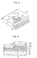
- Fig. 3 shows a perspective view of the resin-molded semiconductor integrated circuit device of the present invention.
- FIG. 3 shows a thin package called an SOP (small outline package) and leads 23 are coated with solder.
- Numeral 20 denotes a semiconductor pellet having a multi-layer wiring structure and numeral 21 denotes a tab for supporting the semiconductor pellet 20. The semiconductor pellet 20 is bonded to the tab 21 by Ag paste.
- Numeral 22 denotes a wire and numeral 24 denotes the resin mold formed by the transfer molding method.
- the resin-molded semiconductor integrated circuit device of the present embodiment was subjected to a reliability test such as a temperature cycle lifetime test.
- Temperature cycle lifetime (Samples to be tested were alternately placed in a high temperature chamber (150°C) and a low temperature chamber ⁇ -55°C) and the occurrence of cracks in the interlayer insulation film was examined).
- the test result shows the number of cracked samples/number of samples tested.
- the soft polyimide resin absorbs the stress created between the molding resin and the semiconductor pellet by the thermal stress and reduces the stress applied to the interlayer insulation film under the polyimide resin.
- no crack occurs in the inorganic interlayer insulation film 14 and the CVD-PSG film 17 (final passivation). Since no crack occurs in the interlayer insulation film at a step D, the first level wiring 13 (lower wiring) and the second level wiring 15 (upper wiring) do not short to each other.
- Another reason for no cracking at the step D may be that the interlayer insulation film includes the SOG deposited by coating. By the use of the SOG film, the step of the interlayer insulation film can be relieved and the crack at the step D is further prevented.
- the present embodiment provides the semiconductor integrated circuit device having a high reliability and a high density wiring structure. Since the anti-thermal stress property is enhanced by the present embodiment, the resin-molded semiconductor integrated circuit device may be dipped in a solder bath when the leads are soldered.
- the polyimide resin film 17b is formed on an entire main surface of a semiconductor wafer 100 shown in Fig. 4, except on scribe-line areas 101 and bonding pad areas (not shown).
- a square block 102 encircled by the scribe lines 101 corresponds to the semiconductor pellet (or called a semiconductor chip) 20 shown in Fig. 3.
- Fig. 5 shows a partial enlarged sectional view (taken along a line X-X of the semiconductor wafer shown in Fig. 4) of the semiconductor wafer 100 in the vicinity of the scribe line 101. As shown in Fig.
- the edges of the Si0 2 film 12 and the interlayer insulation film 14 in the vicinity of the scribe line 101 are coated with the final passivation film comprising the CVD-PSG film 17a and the polyimide resin film 17b. Accordingly, the penetration of the moisture from the edge is prevented and the anti-humidity property is improved.
- the present embodiment further offers the following advantages.
- the semiconductor wafer 101 When the semiconductor wafer 101 is divided into the semiconductor pellets 20, it is diced along the scribe lines 101. Fine particles of the semiconductor wafer scatter during this work, but the second level wiring 15 is protected by the polyimide resin film 17b. Since the polyimide resin film 17b is the soft organic resin film, no crack occurs therein by the fine particles.
- the interlayer insulation film 14 is an inorganic insulative film having a three-layer structure of a plasma Si0 2 film (having a thickness of 200 nm (2,000 A)), an SOG film (having a thickness of 115 nm (1,150 A)) and a CVD-PSG film (having a thickness of 600 nm (6,000 A)), from the bottom to the top.
- the plasma Si0 2 (P-Si0 2 ) film is used instead of the P-SiN film in order to prevent the variation and the deterioration of the electrical characteristic of the MIS FET's.
- the P-Si0 2 film is formed to prevent the hillrock of the aluminum.
- the thickness of the CVD-PSG film 17a used as the final passivation is 200 nm (2,000 A), and the thickness of the polyimide resin film 17b, for example, PIQ is approximately 2.3-3.75 pm.
- a P-SiN film having a thickness of 1.1 pm is interleaved between the CVD-PSG film 17a and the polyimide resin film 17b in order to improve the anti-humidity property.
Landscapes
- Internal Circuitry In Semiconductor Integrated Circuit Devices (AREA)
- Formation Of Insulating Films (AREA)
Description
- The present invention relates to a wiring technique, more particularly to a technique particularly effective to a multi-layer wiring, and to an electronic device having a muti-layer wiring structure such as a resin-molded semiconductor integrated circuit device having a multi-layer wiring structure.
- A semiconductor device having a multi-layer wiring structure has been well known by, for example, U.S. Patent 4,001,870. In this patent, an organic material such as polyimide is used as an interlayer insulation film.
- The polyimide resin, however, has a shortcoming in that it includes moisture and aluminum, if it is used as a wiring material, is corroded by the moisture. Further, since it is difficult to form a thin layer, contact holes in the interlayer insulation film (polyimide resin film) are necessarily large. As a result, the miniaturization is hard to attain.
- Accordingly, a semiconductor integrated circuit device having a high reliability and a high density cannot be obtained.
- In order to provide a semiconductor integrated circuit device having a high reliability and a high density wiring structure, the inventors of the present invention studied the use of a layer structure as disclosed in the laid open German patent application 2 637 667 with an inorganic material such as CVD-PSG (chemical vapor deposition-phosphorus silicate glass) as an interlayer insulation film 4 and a protection layer 6 to protect the topmost wiring layer (second level wiring 5) as shown in Fig. 1. However, the following new problem occurred.
- In order to reduce a cost of the semiconductor integrated circuit device, resin was used as a packaging (molding) material and the resin was package-molded by a well-known transfer mold method. However, since the softened resin is press-inserted into a mold in the transfer mold method, pressures P1, P2 and P3 are applied to the protection layer 6 as shown in Fig. 1, and the protection layer 6 and the interlayer insulation film 4 are cracked by a stress created when the resin is cured and a thermal stress created during a heat cycle test after the resin molding. The cracks occurred at areas B and C of the interlayer insulation film 4 and particularly at a stepped area A. In the stepped area A, many cracks occurred at regions where an edge of the
second level wiring 5 runs closely to an edge of a first level wiring 3. - As a result, moisture penetrated from a portion of the cracked protection layer 6 or a portion of the cracked interlayer insulation film 4 and it eroded the
aluminum wirings 3 and 5 and shorted the first level wiring 3 and thesecond level wiring 5, and the semiconductor integrated circuit device having the high reliabilitywas not provided. In Fig. 1, numeral 1 denotes a semiconductor (Si) substrate and numeral 2 denotes a thermal oxidization film (SiO2 film). - It is an object of the present invention to provide an electronic device having a highly reliable multi-layer wiring structure.
- It is another object of the present invention to provide a highly reliable and high density resin-molded semiconductor integrated circuit device.
- It is another object of the present invention to provide a compact resin-molded semiconductor integrated circuit device.
- It is another object of the present invention to provide a bipolar semiconductor integrated circuit device having a high reliability and a high density.
- The above objects are met by the invention as defined in claim 1.
- The present invention will be apparent from the following detailed description taken in conjunction with the accompanying drawings, in which:
- Fig. 1 is a partial sectional view of a semiconductor integrated circuit device considered priorto the present invention;
- Fig. 2 is a partial sectional view of a resin-molded semiconductor integrated circuit device in accordance with one embodiment of the present invention;
- Fig. 3 is a perspective view of the resin-molded semiconductor integrated circuit device (an external view of a package) of the present invention;
- Fig. 4 is a perspective view of a semiconductor wafer;
- Fig. 5 is a partial, enlarged sectional view of the semiconductor wafer shown in Fig. 4; and
- Fig. 6 is a partial sectional view of a semiconductor integrated circuit device before the resin- molding in accordance with other embodiments of the present invention.
- Fig. 2 shows a partial sectional view of a semiconductor integrated circuit device having a two-layer wiring structure, which is a most typical embodiment of the present invention.
- In Fig. 2,
numeral 10 denotes a substrate of an electronic device. For a bipolar semiconductor integrated circuit device, it is a semiconductor substrate, and more specifically it is an N-type epitaxial semiconductor layer formed on a P-type silicon substrate (not shown). Numeral 11 denotes a P-type semiconductor region selectively formed in the N-typeepitaxial semiconductorlayer 10 by a conventional diffusion technique or ion implantation technique. - In an actual semiconductor integrated circuit device, not only the P-type semiconductor region 11 but also an isolation region and a buried region are formed, although those regions are omitted in Fig. 2. An example of the present semiconductor integrated circuit device is an LS-TTL (low power Schottky transistor-transistor logic) circuit.
- Numeral 12 denotes a silicon dioxide (Si02) film formed by thermally oxidizing the surface of the
epitaxial semiconductor layer 10. The Si02 film 12 is used as a maskfor selectively forming the P-type region 11. Afirst IeveI wiring 13 (having a thickness of 1.0-1.4 itm) is formed on the Si02 film 12. A portion of thewiring 13 contacts to the P-type semiconductor region 11. Pure aluminum is used for thewiring 13. Aninsulation film 14 isformed as an interlayer insulation film on the entire surface of the epitaxial semiconductor layer or thesemiconductor substrate 10 to protect thewiring 13. Theinterlayer insulation film 14 is an inorganic laminated structure of a CVD-PSG film (having a thickness of 600 nm (corresponding to 6000 A)), an SOG (spin-on-glass) film (having a thickness of 200 nm (2000 A)) and a P-SiN (plasma nitride) film (having a thickness of 240 nm (2400 A)). The P-SiN film is first formed to cover thewiring 13. The P-SiN film is used as the interlayer insulation film because of a low defect density such as pinholes. The P-SiN film is also effective to prevent hill-rock of the aluminum (wiring 13). After the formation of thewiring 13, heat treatment called contact alloying (for example, at 470-490°C for 15 minutes) is usually carried out to assure a perfect ohmic contact between thewiring 13 and the semiconductor region. During the heat treatment (contact alloying), the hillrock of the aluminum occurs. However, when the P-SiN film is formed and then the contact alloying is carried out, the hillrock is prevented by the P-SiN film. The thickness of the P-SiN film is preferably 100 nm-300 nm (1000 A-3000 A). The SOG film or the insulative glass film is formed on the P-SiN film by a rotating coating method. If the SOG film is too thick, a crack will occur therein. Accordingly, the thickness is preferably 80 nm-200 nm (800 Ä2000 A). The CVD-PSG film is formed on the SOG film. The CVD-PSG film is used to passivate the semiconductor surface by a gettering effect of phosphorous. The thickness of the CVD-PSG film is preferably 500 nm-1000 nm (5000 A-10000 A). A concentration of P205 contained in the CVD-PSG film is preferably 4-6 mol%. In the present embodiment, it is 6 mol%. - A second level wiring 15 (having a thickness of 1.7-2.0 pm) and a
bonding pad 16 formed by simultaneous patterning with thewiring 15 are formed on the laminatedinterlayer insulation film 14. Aluminum containing Si is used for thewiring 15 and thebonding pad 16 for anti-corrosion purpose. The aluminum containing the Si is deposited by a sputtering method to improve a step coverage. A CVD-PSG film 17a (having a thickness of 120 nm (1200 A)) is formed as a final passivation layer on thewiring 15, and anorganic resin film 17b such as a polyimide resin film (having a thickness of approximately 3.8 pm) is formed on the CVD-PSG film in accordance with the feature of the present invention. Polyimide isoindro quinazolinedione (PIQ, trademark of Hitachi Chemical Co., Ltd.) is preferable for thepolyimide resin film 17b. The CVD-PSG film 17a formed for final passivation underlying thepolyimide resin film 17b is intended to protect thesecond level wiring 15 by the relatively hard passivation film so that it is not broken by the pressure during the molding. It also serves to enhance anti-humidity property. If the polyimide resin is deposited directly on thesecond level wiring 15, thewiring 15 may be broken by displacement by the pressure during the molding because the polyimide resin is soft. Further, since the polyimide resin contains moisture, the aluminum may be eroded. Accordingly, the CVD-PSG film 17a is formed on thewiring 15 to prevent the above problems. A concentration of P205 contained in the CVD-PSG film 17a to prevent the deterioration of the anti-humidity property is 4 mol% which is lower than the concentration of P201 in the CVD-PSG used as the interlayer insulation film. While not shown, a CVD-Si02 film having a thickness of approximately 200 nm (2000 A) is formed between the CVD-PSG film 17a and the polyimide resin film in order to further prevent the deterioration of the anti-humidity property and maintain an appropriate hardness. The thickness of the polyimide resin film need not be very large and preferably 4-6 pm, taking an etching time into consideration. The CVD-PSG film 17a and thepolyimide resin film 17b are selectively etched through a common pattern mask to expose thebonding pad 16. AnAu wire 18 or an AI wire is bonded to thebonding pad 16 by a nail head bonding or ultrasonic bonding method. The other end of the wire is bonded to an end of a lead (not shown). This will be readily understood from the explanation of Fig. 3 to be made later. The wire-bonded electronic device or semiconductor pellet is molded or packaged by a thermo-settingresin 19 such as epoxy resin composition. The packaging may be done by a well-known transfer mold method. Fig. 3 shows a perspective view of the resin-molded semiconductor integrated circuit device of the present invention. Fig. 3 shows a thin package called an SOP (small outline package) and leads 23 are coated with solder.Numeral 20 denotes a semiconductor pellet having a multi-layer wiring structure and numeral 21 denotes a tab for supporting thesemiconductor pellet 20. Thesemiconductor pellet 20 is bonded to thetab 21 by Ag paste.Numeral 22 denotes a wire and numeral 24 denotes the resin mold formed by the transfer molding method. - The resin-molded semiconductor integrated circuit device of the present embodiment was subjected to a reliability test such as a temperature cycle lifetime test.
- Temperature cycle lifetime (Samples to be tested were alternately placed in a high temperature chamber (150°C) and a low temperature chamber <-55°C) and the occurrence of cracks in the interlayer insulation film was examined).
-
- Samples A (comparative samples
- having final passivation films
- consisting of the CVD-PSG) 30
- Sample B (inventive samples
- having the final passivation films of
- thetwo-layerstructureofCVD-PSGand
- PIQ) 30

- The test result shows the number of cracked samples/number of samples tested.
- As seen from the above test result, according to the present invention, the soft polyimide resin absorbs the stress created between the molding resin and the semiconductor pellet by the thermal stress and reduces the stress applied to the interlayer insulation film under the polyimide resin. As a result, no crack occurs in the inorganic
interlayer insulation film 14 and the CVD-PSG film 17 (final passivation). Since no crack occurs in the interlayer insulation film at a step D, the first level wiring 13 (lower wiring) and the second level wiring 15 (upper wiring) do not short to each other. Another reason for no cracking at the step D may be that the interlayer insulation film includes the SOG deposited by coating. By the use of the SOG film, the step of the interlayer insulation film can be relieved and the crack at the step D is further prevented. - Accordingly, the present embodiment provides the semiconductor integrated circuit device having a high reliability and a high density wiring structure. Since the anti-thermal stress property is enhanced by the present embodiment, the resin-molded semiconductor integrated circuit device may be dipped in a solder bath when the leads are soldered.
- In the present embodiment, the
polyimide resin film 17b is formed on an entire main surface of asemiconductor wafer 100 shown in Fig. 4, except on scribe-line areas 101 and bonding pad areas (not shown). Asquare block 102 encircled by the scribe lines 101 corresponds to the semiconductor pellet (or called a semiconductor chip) 20 shown in Fig. 3. Fig. 5 shows a partial enlarged sectional view (taken along a line X-X of the semiconductor wafer shown in Fig. 4) of thesemiconductor wafer 100 in the vicinity of thescribe line 101. As shown in Fig. 5, the edges of the Si02 film 12 and theinterlayer insulation film 14 in the vicinity of thescribe line 101 are coated with the final passivation film comprising the CVD-PSG film 17a and thepolyimide resin film 17b. Accordingly, the penetration of the moisture from the edge is prevented and the anti-humidity property is improved. - The present embodiment further offers the following advantages.
- When the
semiconductor wafer 101 is divided into thesemiconductor pellets 20, it is diced along the scribe lines 101. Fine particles of the semiconductor wafer scatter during this work, but thesecond level wiring 15 is protected by thepolyimide resin film 17b. Since thepolyimide resin film 17b is the soft organic resin film, no crack occurs therein by the fine particles. - Since the main surface of the semiconductor pellet is protected by the soft organic resin film, the handling of the semiconductor pellet is very easy.
- While the preferred embodiment of the present invention has been described in detail, the present invention is not limited to the above embodiment but various modifications may be made without departing from the scope of the invention. For example, the following modifications may be made.
- (a) Fig. 6 shows a partial sectional view of a semiconductor integrated circuit device having a multi-layer wiring structure in accordance with other embodiments of the present invention. In the semiconductor integrated circuit device of Fig. 6, an insulative glass film such as
SOG film 17c is interposed between the CVD-PSG film 17a and thepolyimide resin film 17b. By interposing theglass film 17c, the step is relieved so that the cracking in the interlayer insulation film is further prevented. This final passivation structure (17a, 17c, 17b) is effectively applicable to the three-layer or multi-layer wiring structure having a steep step. - (b) In the above embodiment, the polyimide resin is formed prior to the wire bonding. In the present embodiment, the final passivation comprises only the CVD-PSG film, and the polyimide resin is coated by potting on the main surface of the semiconductor pellet after the wire bonding and before the molding.
- (c) In the above embodiment, the semiconductor region formed in the semiconductor substrate forms the bipolar IC. Alternatively, the semiconductor region may form a MIS IC (or also called MOS IC). It may also form a Bi-MOS IC which contains the bipolar IC and the MOS IC in one semiconductor substrate. The multi-layer wiring structure of the semiconductor integrated circuit device which contains MIS FET's such as the MIS IC or the Bi-CMOSIC is explained with reference to Fig. 2.
- In Fig. 2, the thickness of the
first level wiring 13 and the second level wiring 15 (bonding pad 16) is 0.8 pm. Theinterlayer insulation film 14 is an inorganic insulative film having a three-layer structure of a plasma Si02 film (having a thickness of 200 nm (2,000 A)), an SOG film (having a thickness of 115 nm (1,150 A)) and a CVD-PSG film (having a thickness of 600 nm (6,000 A)), from the bottom to the top. In the semiconductor integrated circuit device which contains the MIS FET's, the plasma Si02 (P-Si02) film is used instead of the P-SiN film in order to prevent the variation and the deterioration of the electrical characteristic of the MIS FET's. Like the P-SiN film, the P-Si02 film is formed to prevent the hillrock of the aluminum. The thickness of the CVD-PSG film 17a used as the final passivation is 200 nm (2,000 A), and the thickness of thepolyimide resin film 17b, for example, PIQ is approximately 2.3-3.75 pm. A P-SiN film having a thickness of 1.1 pm is interleaved between the CVD-PSG film 17a and thepolyimide resin film 17b in order to improve the anti-humidity property. - (d) Photosensitive polyimide may be used for the
polyimide resin film 17b. No photo-resist is required for the photosensitive polyimide in the selective etching process. Accordingly, the number of steps can be reduced by the use of the photosensitive polyimide. - (e) One resin selected from silicone resin, imide silicone resin, teflon and polyethylene, or a combination thereof may be used as the
final passivation film 17b to form the multi-layer structure film.
Claims (6)
characterized in that a phosphorus silicate glass film (17a) is formed between said upper wiring and said organic resin film.
Applications Claiming Priority (2)
| Application Number | Priority Date | Filing Date | Title |
|---|---|---|---|
| JP58065337A JPS59191353A (en) | 1983-04-15 | 1983-04-15 | Electronic device having multilayer interconnection structure |
| JP65337/83 | 1983-04-15 |
Publications (3)
| Publication Number | Publication Date |
|---|---|
| EP0122631A2 EP0122631A2 (en) | 1984-10-24 |
| EP0122631A3 EP0122631A3 (en) | 1986-09-10 |
| EP0122631B1 true EP0122631B1 (en) | 1990-10-31 |
Family
ID=13284011
Family Applications (1)
| Application Number | Title | Priority Date | Filing Date |
|---|---|---|---|
| EP19840104298 Expired - Lifetime EP0122631B1 (en) | 1983-04-15 | 1984-04-16 | Electronic device having a multi-layer wiring structure |
Country Status (6)
| Country | Link |
|---|---|
| EP (1) | EP0122631B1 (en) |
| JP (1) | JPS59191353A (en) |
| KR (1) | KR870000350B1 (en) |
| DE (1) | DE3483488D1 (en) |
| HK (1) | HK20793A (en) |
| SG (1) | SG102492G (en) |
Families Citing this family (15)
| Publication number | Priority date | Publication date | Assignee | Title |
|---|---|---|---|---|
| US4693780A (en) * | 1985-02-22 | 1987-09-15 | Siemens Aktiengesellschaft | Electrical isolation and leveling of patterned surfaces |
| JPH0652732B2 (en) * | 1985-08-14 | 1994-07-06 | 三菱電機株式会社 | Method for forming passivation film |
| ATE67897T1 (en) * | 1985-10-22 | 1991-10-15 | Siemens Ag | INTEGRATED SEMICONDUCTOR CIRCUIT WITH AN ELECTRICALLY CONDUCTIVE SURFACE ELEMENT. |
| EP0275588B1 (en) * | 1986-12-19 | 1993-11-10 | Koninklijke Philips Electronics N.V. | Method of fabricating a semiconductor device with reduced packaging stress |
| US5171716A (en) * | 1986-12-19 | 1992-12-15 | North American Philips Corp. | Method of manufacturing semiconductor device with reduced packaging stress |
| JP2631659B2 (en) * | 1987-07-09 | 1997-07-16 | 富士通株式会社 | Semiconductor device |
| JPH01214141A (en) * | 1988-02-23 | 1989-08-28 | Nec Corp | Flip-chip type semiconductor device |
| US5252844A (en) * | 1988-11-17 | 1993-10-12 | Mitsubishi Denki Kabushiki Kaisha | Semiconductor device having a redundant circuit and method of manufacturing thereof |
| JPH02256258A (en) * | 1988-11-17 | 1990-10-17 | Mitsubishi Electric Corp | Manufacture of semiconductor device |
| NL8900989A (en) * | 1989-04-20 | 1990-11-16 | Philips Nv | SEMICONDUCTOR DEVICE WITH A SEMICONDUCTOR BODY EMBEDDED IN A PLASTIC COVER. |
| NL9100337A (en) * | 1991-02-26 | 1992-09-16 | Philips Nv | SEMICONDUCTOR DEVICE. |
| GB2279804A (en) * | 1993-07-02 | 1995-01-11 | Plessey Semiconductors Ltd | Insulating layers for multilayer wiring |
| US5438022A (en) | 1993-12-14 | 1995-08-01 | At&T Global Information Solutions Company | Method for using low dielectric constant material in integrated circuit fabrication |
| KR100582371B1 (en) * | 1999-12-24 | 2006-05-23 | 주식회사 하이닉스반도체 | Metal Wiring of Semiconductor Devices and Formation Method |
| JP2001284499A (en) * | 2000-03-09 | 2001-10-12 | Lucent Technol Inc | Semiconductor device and manufacturing method thereof |
Family Cites Families (5)
| Publication number | Priority date | Publication date | Assignee | Title |
|---|---|---|---|---|
| US4001871A (en) * | 1968-06-17 | 1977-01-04 | Nippon Electric Company, Ltd. | Semiconductor device |
| JPS5851425B2 (en) * | 1975-08-22 | 1983-11-16 | 株式会社日立製作所 | Hand tie souchi |
| EP0021818B1 (en) * | 1979-06-21 | 1983-10-05 | Fujitsu Limited | Improved electronic device having multilayer wiring structure |
| US4433004A (en) * | 1979-07-11 | 1984-02-21 | Tokyo Shibaura Denki Kabushiki Kaisha | Semiconductor device and a method for manufacturing the same |
| JPS5768059A (en) * | 1980-10-15 | 1982-04-26 | Mitsubishi Electric Corp | Semiconductor device |
-
1983
- 1983-04-15 JP JP58065337A patent/JPS59191353A/en active Pending
-
1984
- 1984-04-12 KR KR1019840001937A patent/KR870000350B1/en not_active Expired
- 1984-04-16 EP EP19840104298 patent/EP0122631B1/en not_active Expired - Lifetime
- 1984-04-16 DE DE8484104298T patent/DE3483488D1/en not_active Expired - Lifetime
-
1992
- 1992-10-07 SG SG102492A patent/SG102492G/en unknown
-
1993
- 1993-03-11 HK HK207/93A patent/HK20793A/en not_active IP Right Cessation
Also Published As
| Publication number | Publication date |
|---|---|
| DE3483488D1 (en) | 1990-12-06 |
| KR840008535A (en) | 1984-12-15 |
| HK20793A (en) | 1993-03-19 |
| EP0122631A3 (en) | 1986-09-10 |
| JPS59191353A (en) | 1984-10-30 |
| KR870000350B1 (en) | 1987-03-04 |
| EP0122631A2 (en) | 1984-10-24 |
| SG102492G (en) | 1992-12-24 |
Similar Documents
| Publication | Publication Date | Title |
|---|---|---|
| US5300461A (en) | Process for fabricating sealed semiconductor chip using silicon nitride passivation film | |
| US5861658A (en) | Inorganic seal for encapsulation of an organic layer and method for making the same | |
| US4472730A (en) | Semiconductor device having an improved moisture resistance | |
| US6727590B2 (en) | Semiconductor device with internal bonding pad | |
| US5661082A (en) | Process for forming a semiconductor device having a bond pad | |
| US5539257A (en) | Resin molded type semiconductor device having a conductor film | |
| US6025277A (en) | Method and structure for preventing bonding pad peel back | |
| EP0122631A2 (en) | Electronic device having a multi-layer wiring structure | |
| US6028347A (en) | Semiconductor structures and packaging methods | |
| CN104617043A (en) | Component Manufacturing Method | |
| US7224060B2 (en) | Integrated circuit with protective moat | |
| US20040245642A1 (en) | Semiconductor device | |
| TWI397972B (en) | Semiconductor device manufacturing method | |
| JPH04279050A (en) | Semiconductor device and manufacture thereof | |
| US5229642A (en) | Resin molded type semiconductor device having a conductor film | |
| US6248657B1 (en) | Semiconductor device and method for manufacturing the same | |
| US5552639A (en) | Resin molded type semiconductor device having a conductor film | |
| US20220013481A1 (en) | Semiconductor device and method of manufacturing the same | |
| GB2134709A (en) | Semiconductor device and fabrication method thereof | |
| US10892239B1 (en) | Bond pad reliability of semiconductor devices | |
| US8809695B2 (en) | Contact structure for an electronic circuit substrate and electronic circuit comprising said contact structure | |
| US5187558A (en) | Stress reduction structure for a resin sealed semiconductor device | |
| JPS5974651A (en) | Semiconductor device | |
| JPH038583B2 (en) | ||
| US7498194B2 (en) | Semiconductor arrangement |
Legal Events
| Date | Code | Title | Description |
|---|---|---|---|
| PUAI | Public reference made under article 153(3) epc to a published international application that has entered the european phase |
Free format text: ORIGINAL CODE: 0009012 |
|
| AK | Designated contracting states |
Designated state(s): DE FR GB IT |
|
| 17P | Request for examination filed |
Effective date: 19841220 |
|
| PUAL | Search report despatched |
Free format text: ORIGINAL CODE: 0009013 |
|
| AK | Designated contracting states |
Kind code of ref document: A3 Designated state(s): DE FR GB IT |
|
| 17Q | First examination report despatched |
Effective date: 19880811 |
|
| GRAA | (expected) grant |
Free format text: ORIGINAL CODE: 0009210 |
|
| AK | Designated contracting states |
Kind code of ref document: B1 Designated state(s): DE FR GB IT |
|
| REF | Corresponds to: |
Ref document number: 3483488 Country of ref document: DE Date of ref document: 19901206 |
|
| ET | Fr: translation filed | ||
| ITF | It: translation for a ep patent filed | ||
| ITTA | It: last paid annual fee | ||
| RAP2 | Party data changed (patent owner data changed or rights of a patent transferred) |
Owner name: HITACHI MICROCOMPUTER SYSTEM LTD. Owner name: HITACHI, LTD. |
|
| PLBE | No opposition filed within time limit |
Free format text: ORIGINAL CODE: 0009261 |
|
| STAA | Information on the status of an ep patent application or granted ep patent |
Free format text: STATUS: NO OPPOSITION FILED WITHIN TIME LIMIT |
|
| 26N | No opposition filed | ||
| ITPR | It: changes in ownership of a european patent |
Owner name: CAMBIO RAGIONE SOCIALE;HITACHI MICROCOMPUTER SYSTE |
|
| REG | Reference to a national code |
Ref country code: FR Ref legal event code: CD |
|
| PGFP | Annual fee paid to national office [announced via postgrant information from national office to epo] |
Ref country code: GB Payment date: 19960404 Year of fee payment: 13 |
|
| PGFP | Annual fee paid to national office [announced via postgrant information from national office to epo] |
Ref country code: DE Payment date: 19960627 Year of fee payment: 13 |
|
| PGFP | Annual fee paid to national office [announced via postgrant information from national office to epo] |
Ref country code: FR Payment date: 19970217 Year of fee payment: 14 |
|
| PG25 | Lapsed in a contracting state [announced via postgrant information from national office to epo] |
Ref country code: GB Effective date: 19970416 |
|
| GBPC | Gb: european patent ceased through non-payment of renewal fee |
Effective date: 19970416 |
|
| PG25 | Lapsed in a contracting state [announced via postgrant information from national office to epo] |
Ref country code: DE Free format text: LAPSE BECAUSE OF NON-PAYMENT OF DUE FEES Effective date: 19980101 |
|
| PG25 | Lapsed in a contracting state [announced via postgrant information from national office to epo] |
Ref country code: FR Free format text: THE PATENT HAS BEEN ANNULLED BY A DECISION OF A NATIONAL AUTHORITY Effective date: 19980430 |
|
| REG | Reference to a national code |
Ref country code: FR Ref legal event code: ST |