EP0120745A1 - Apparatus permitting memory access timesharing by a plurality of users - Google Patents
Apparatus permitting memory access timesharing by a plurality of users Download PDFInfo
- Publication number
- EP0120745A1 EP0120745A1 EP84400381A EP84400381A EP0120745A1 EP 0120745 A1 EP0120745 A1 EP 0120745A1 EP 84400381 A EP84400381 A EP 84400381A EP 84400381 A EP84400381 A EP 84400381A EP 0120745 A1 EP0120745 A1 EP 0120745A1
- Authority
- EP
- European Patent Office
- Prior art keywords
- memory
- access
- signal
- cycle
- cas
- Prior art date
- Legal status (The legal status is an assumption and is not a legal conclusion. Google has not performed a legal analysis and makes no representation as to the accuracy of the status listed.)
- Granted
Links
Images

Classifications
-
- G—PHYSICS
- G09—EDUCATION; CRYPTOGRAPHY; DISPLAY; ADVERTISING; SEALS
- G09G—ARRANGEMENTS OR CIRCUITS FOR CONTROL OF INDICATING DEVICES USING STATIC MEANS TO PRESENT VARIABLE INFORMATION
- G09G5/00—Control arrangements or circuits for visual indicators common to cathode-ray tube indicators and other visual indicators
- G09G5/001—Arbitration of resources in a display system, e.g. control of access to frame buffer by video controller and/or main processor
-
- G—PHYSICS
- G06—COMPUTING; CALCULATING OR COUNTING
- G06F—ELECTRIC DIGITAL DATA PROCESSING
- G06F12/00—Accessing, addressing or allocating within memory systems or architectures
- G06F12/02—Addressing or allocation; Relocation
- G06F12/0207—Addressing or allocation; Relocation with multidimensional access, e.g. row/column, matrix
Definitions
- the instant invention relates to a device for distributing a memory access time among a plurality of users.
- the CPU which has first priority and each time that it requests access to the memory, it will receive memory cycle time either immediately, if no other cycle is in progress, or in the following cycle, if a current cycle is assigned to another user, the access demands of other users being held on wait and subsequently processed as a function of their priority. During this process, a user having a higher priority can always intervene to request access which will be obtained over a request of a user having a lower priority.
- DMA circuits (this abreviation will be used hereinafter to designate the circuit according to the invention) provide for memory exploitation with great efficiency despite the presence of a plurality of users.
- the duration of the cycles which-are processed by the DMA cannot be shorter than those of the memory itself which are determined by the particular technology of the system.
- memories integrated on semi-conductor chips consist of matrixes of memory cells distributed in rows and columns, which are addressed by row and column addresses.
- the construction of these memories is such that there is required, for a column or row addressing cycle, a certain "preloading" time necessary for placing the circuits associated with the matrix into the condition of selected read/write.
- the preloading time of the rows is generally substantially longer than the column preloading time. For example, for a memory access cycle of 250 ns, a time period which is usual in currently available RAM memories, there is required a preloading time of 100 ns for the rows, while, for the columns, a few dozen ns will be sufficient.
- each row can have a plurality of bytes of memory cells which are addressed separately by the column addresses so that each time it is desired to address a predetermined byte, there will be a complete memory cycle having a long access time for the rows and a short access time for the columns. Consequently, when a memory zone of the RAM is loaded at all of these successive addresses, for example in the case of a page memory of a cathode ray tube visualization system, it is necessary to execute for each address a complete memory cycle, which entails that the "row" access time uses up a very large portion of the total time for writing into or reading in the memory.
- E-P-A 0,087,868,published after the priority date of the present application discloses a graphics display refresh memory architecture wherein several address location of the memory can be addressed with several column address strobe signals while using only one row address strobe signal.
- the memory is coupled to only one user and no priority can thus be allocated for accessing the memory.
- the invention has as an object a control circuit which provides a better distribution, among a plurality of users, of the access time to a memory while also reducing, to the minimum, the reading and writing time of the information into or in the matrix of this memory.
- the invention has as an object an asynchronous control device adapted to access by a plurality of users to a RAM memory, the access of which is controlled by row (RAS) and column (CAS) strobe signals accompanying respectively the row and column addresses which identify the cells of the memory matrix, wherein a read/write operation is to be effected,
- this device being characterized in that it comprises in combination, for each user, a processing path for the access requests presented by the users, the processing paths being interconnected in such a manner that the access requests are granted with the priority with which the users are classified for memory access, the device also including a generator circuit which, from the time an access request is presented, generates a signal (CYCLE), the duration of which determines a complete access cycle of the memory under control of said signals (RAS,CAS), and means in said circuit generator of said duration signal for allocating to at least certain of said users, a plurality of column strobe signals for a single row strobe signal.
- RAS row
- CAS column
- each complete memory access cycle can be executed by a single row cycle, at the corresponding row address, by means of a row enabling signal, which is maintained during the row preloading time and throughout the duration of one or more column cycles executed with the column addresses which is progressively incremented, and enabled by at least one column'validation signal, the number of column cycles per row cycles being determined by the users of the memory.
- Figure l A shows a timing diagram of a simple memory access cycle.
- a RAS signal row address strobe
- a CAS signal column address strobe
- Figure l A relates for example to communications between a central processing unit CPU and the memory, wherein each read/write operation entails addressing of a single memory cell.
- the memory user is a circuit which requests, for example, the writing of a series of data at numerous successive addresses in the memory, which is the case, for example, of a page memory memorizing an image for each frame to be displayed on the screen of a sweeped frame cathode ray tube.
- the data are successively written into the memory at the addres- ses starting at the beginning of a row (first byte) , after which the other bytes of the row are filled u p , one after another, by incrementation of the column address.
- the row address is incremented by one unit to permit the loading of the following row of the memory matrix. It is clear that if there is utilized the conventional addressing system of Figure 1A, each loading of a byte requires the sum of a preloading time RAS and a preloading time CAS while, actually, the row address does not change. For this reason, the invention utilizes, in such a case, only one single row addressing for a plurality of column ad- dressings which is seen in Figure 1B.
- the signal CYCLE is maintained as long as a memory row is loaded, the signal RAS being generated only a single time during this operation and also maintained during the entire cycle.
- the signal CAS is repeated as many times as necessary (for example, the number of columns which are in the memory). Because of this control, the time for storing- data into a row is substantially shorter and considerable memory access time can be saved.
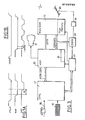
- Figure 2 shows a DMA circuit which allows the obtainment of an access, in time sharing, to a memory which, according to the type of user, is "monocycle" ( Figure l A ) or “multicycle” ( Figure 1B ) .
- the DMA circuit includes an asynchronous control logic circuit 1 which produces on its outputs Sl, S2, S3, cycle signals adapted to allocate to the users U1, U2, U3, an access time to the RAM memory, as a function of the access requests which the users present during the operation.
- the access request signals are applied to inputs El, E2 and E3 by the users.
- the asynchronous control logic circuit includes three essential parts, namely a preliminary memorization circuit 2, for the access requests, which is connected to a memorization circuit 3 for access requests in progress, this circuit 3 being, in turn, connected to a priority logic 4.
- a preliminary memorization circuit 2 for the access requests
- memorization circuit 3 for access requests in progress
- this circuit 3 being, in turn, connected to a priority logic 4.
- control logic circuit is a three path circuit. There is no phase relation among the three paths.
- the outputs of the circuits 2a, 2b, 2 c are connected to the inputs of a NOR gate 5, the output of which is connected to the input of a processing circuit 6 for the RAS and CAS signals.
- This circuit 6 is connected, on the one hand, to memorization circuits 3a, 3b, 3c for access requestsin progress, and, on the other hand, to an input of each of three NAND gates 4a, 4b, 4c constituting the three paths of the logic priority circuit 4,by lines Ll and L2 on which circulate the signals "start cycle” and "cycle” respectively.
- Gate 4a is a two input gate, one input being connected to a first output of circuit 3a, the other connected to line L2.
- Gate 4b is a three input gate, one input connected to a line L2, another connected to a second output of circuit 3 a, and another to the first output of circuit 3b.
- Gate 4c is a four input gate, one input connected to line L2, and the others connected to outputs of circuits 3a, 3b, 3c.
- the circuit thus constructed stores the requests for access to the memory and classifies the requests according to an arrival order or a priority order.
- path E1S1 has the highest priority
- path E2S2 requires an access of the "multicycle” type
- the paths E1S1 and E3S3 require only "monocycle" access.
- the RS flip-flop 2a changes state, so that the input D1 of circuit 3a goes to 1, which entails the changing of the state of the output of NOR gate 5, which causes, by means of circuit 6 to be described hereinafter, the appearance of a pulse on line L1.
- the leading edge of this pulse is used to store the access request in the D-type flip-flop 3a, the output Q1 of which goes to a high level.
- NOR gate 5 The output of NOR gate 5 is connected to clock 7 which is triggered when a signal is generated at the output of this gate.
- This clock is connected to two counters 8 and 9 of the RASand CAS signals, respectively. These are connected to decoders 10 and 11, decoder 10 providing a signal "BEGIN CYCLE” ( line L1 ) and a signal “CYCLE” (line L2) and a signal RAS. Decoder 11 generates a CAS signal.
- the RAS and CAS signals are sent along the appropriate lines to row address buffer 12 and column address buffer 13 for enabling the addresses which were loaded therein from an address bus B connected to users U1, U2, U3, the bus of user U2 being the only one represented in the Figure.
- the address buffers are connected to RAM 14.
- the clock Upon reception of a signal from NOR gate 5, the clock starts control of counter 8 which, after having received a number of pulses corresponding to the row preloading time (duration D), triggers counter 9 over line L3. Decoder 10 produces signals BEGIN CYCLE and CYCLE, this latter signal being maintained while RAS counter 8 continues to accumulate clock pulses. The CAS counter counts up according to the rate of these clock pulses, generating the CAS signal through decoder 10. After having counted the number of pulses corresponding to the duration of a RAS cycle, counter 9 sends a reset signal RAZ on line L4 to clock 7, which stops the clock.
- the row and column address buffers 12 and 13 have transferred the corresponding addresses in RAM 14 during the RAS and CAS signals, the RAS counter 8 is reset by line L4, the signal CYCLE is cancelled and gate 4a is disabled. At the same time, flip-flop 2a is reset.
- User U2 is assumed to load memory 14 with a plurality of successive column addresses by a single row address.
- the number of CAS cycles can be controlled by the user itself, the appropriate signal being provided on line L5 which connects user U2 to a cycle number register 15.
- This register is enabled by the signal appearing on lead S2 when the output of gate 4b appears after a memory access request on lead E2 from user U2.
- the cycle number is loaded into register 15 and it is decremented by a unit each time the CAS signal is produced by counter 9. As long as register 15 is not emptied, it produces at its output (conductor L6), a signal which inhibits, in counter 9, the output producing the reset signal on line L4.
- the production of the signal on lead S2 takes place in an identical manner to that of the signal on lead S1, with appropriate priority being, of course, taken into consideration.
- Figure 2 circuit allows for the control, in time sharing, of the access to the memory by a plurality of users, and this totally asynchronously and with regard to a particular priority assigned to the users.
- the users can be part of the same data processing system using a common RAM memory.
- a particularly appropriate application of the invention is in the field of teletext systems.
- Figure 3 shows a very simplified diagram of a terminal for a teletext display utilizing, for example, the "antiope" system.
- Such a terminal includes a central processing unit CPU 17 which receives instructions and information from a plurality of sources 18 and 19, such as a telephone line or a keyboard.
- the CPU 17 cooperates with video display processor VDP 20, which prepares the image information by transforming it into a form which can be utilized by a sweep ed frame cathode ray tube 21.
- the CPU 17 and the VDP 20 cooperate with a mixed RAM/ROM memory 22, by means of an address bus and a data bus.
- Circuit 23, of the "didon" type can communicate with the terminal from a receptor station 24 and antenna 25, receiving a television type signal with interlaced teletext information.
- the VDP 20 includes a decoder circuit 26 which, depending upon the addresses received from the CPU 17, enables the registers (not shown) of the VDP by placing them selectively into the several function modes of image com p o-sition, memory loading, video information reception, memory refreshing, etc.
- access control circuit 27 constituted in accordance with the invention, such as the circuit of Figure 2, it being understood that the circuit here specifically applies to a teletext terminal of the Figure 3 type.
- the access to the memory is here also controlled in an asynchronous manner, as a function of a priority which is established in the following manner :
- priorities 3 and 4 entail a loading or a reading of a series of successive bytes which is a case of multicycle operation 8 as described above.
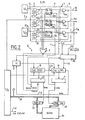
- the access control circuit of Figure 4 includes essentially the same elements as Figure 2 and these elements have the same reference numbers. There will now be described the elements specifically added for the teletext terminal application.
- the cycle number register 15 is here made up of two registers 28 and 29, one for storing a number of "memory planes" and the other for storing a number of writing cycles to be effected when the multicycles are to be effected respectively by paths 3 and 4 of the access control circuit.
- the registers 28 and 29 are enabled by signals S3 and S4, respectively, their enabling inputs being connected by lines L7 and L8 to the corresponding leads S3 and S4.
- Each of the registers includes a zero output, on which appears a signal when the register is empty,for authorizing the production of the RAZ signal applied to the CAS counter, as described in regard to register 15.
- the registers 28 and 29 are decremented by NAND gates 30 and 31 which are enabled by the CAS signals and the respective signals X1 and X2 from comparator 32.
- This comparator includes two sets of inputs which are connected to outputs RS1 - RS4 of the flip-flops 2a-2d and to the outputs of NAND gates 4a - 4d for comparing the logic levels, and thus, the state of the access requests effected with the access cycles in the course of execution.
- Comparator 32 has outputs X1 and X2 connected to gates 39 and 41 and an output INT.which is connected to NOR gate 33, the output of which resets counters 8 and 9 over line L9.
- This resetting can also be ordered by a signal OVERFLOW on line L10 from the arithmetic and logic unit (not shown) of VDP 20.
- This signal is generated when an address is loaded into the location of a row corresponding to the last column of the memory. In this case, the loading is interrupted, the row address is incremented, and the loading is restarted with a new column address corresponding to the first cell of the following row designated by the incremented row address.
- This signal INT is also combined with the CAS signal in NAND gate 34 which in turn is connected to NOR gate 35, receiving the signal BEGIN CYCLE generated at the proper moment by decoder 10.
- the signal CYCLE produced by the decoder 10 is at "1" during the cycle and enables gate C1 for generating a control signal for circuit 26, which places the appropriate elements of VDP 20 ( Figure 3) into a configuration permitting the direct reading into the memory by the CPU.
- the output signal of gate 4a is also sent to flip-flop RS1 at the end of the cycle.
- control signal S1, S2, S3 or S4 having the highest priority (here, in increasing priority, C1-C2-C3-C4).
- Such a request entails, for example, the reading in or writing into in the page memory of a large number of bits.
- each bit belongs to a predetermined "memory plane".
- the term "memory plane” is utilized here to designate a group of memorized bytes, or bytes to be memorized, all of them relating to a predetermined color to be displayed. For example, there can be a red, blue or green memory plane, the bytes of each plane not being necessarily contiguous with each other in the memory.
- the starting of the multicycle is identical to that of the monocycle, however, during the production of signal S3 (or S4), registers 28 or 29 are loaded with a value which, for path 3, is a number of memory planes and, for path 4, a number of CAS cycles. In both cases, a single RAS cycle is necessary for a plurality of CAS cycles. In other words, the CAS signal is repeated, with its preloading time, as long as counter 28 or 29 does not count down to O because of decrementation by the CAS signal. This decrementation is enabled each time by . signals X1 and X2 via gates 39 and 31 for interrupting the execution of the following group of CAS cycles when a higher priority request is present. This point will be returned to in regard to Figured
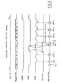
- Figure 5 shows a timing diagram of a multicycle execution with 6 memory planes, this number 6 being stored in counter 28.
- the same Figure 5 illustrates the passage from one row to another when the column address corresponds to the last address of a row (here when counter 28 has been decremented twice).
- the ALU of the VDP 20 provides the OVERLOAD signal which, by means of gate 33, resets counters 8 and 9 to O, in synchronism with clock 7 for a new RAS cycle.
- the address 'of the row is incremented by one unit, and the new CAS cycles are executed successively, until the counter 28 reaches O.
- path 2 allows the reception of exterior data, which data provide the information to be displayed, and this path is essential if one does not wish to lose the message information to be transmitted.
- path 2 (didon circuit 23) requests writing into the memory of a byte each 1.3 microseconds, and such a byte must not be lost.
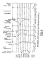
- the DMA circuit according to the invention can interrupt a multicycle request in the process of execution if a higher priority path requests access to the memory. This is seen in Figure 6.
- the circuit initially satisfies, a request on path 4 to execute writing by the CPU into the memory.Thus, three CAS cycles are executed.
- a request on path 4 to execute writing by the CPU into the memory.Thus, three CAS cycles are executed.
- another request is presented on path 3 which causes the production of the INT signal, applied to gate 33, by comparator 32.
- This comparator continually compares the state of flip-flops RS1 - RS4 (requests made), with the state of the outputs of gates Cl - C4 (cycles in the process of execution).
- the comparator If the binary number applied to inputs RS of comparator 32 is not higher than those on inputs C, the comparator produces the INT signal resetting counters 8 and 9 and precluding any new transfer of the CAS signal through gates 30 and 31 by the X 1 and X2 signals..
- the INT signal as the OVERFLOW signal previously, generates the HD-signal which allows storing of the new state of the RS flip-flops
- the DMA circuit provides for access in two cycles to path 3 (in the case represented in Figure 6), after which another request having an even higher priority is presented. After a memory cycle permitting the memorization of a bit of path 2(didon), another higher priority request is presented by the CPU (reading).
- path 3 in the case represented in Figure 6
- Another higher priority request is presented by the CPU (reading).
- two CAS cycles of path 3 which were not executed p re- viously when the request of path 2 was presented, four cycles of the path 3 initiated by the new access request of this path, then, the return to the cycles of path 4 in a plurality of cycles.
- the number of CAS cycles remaining to be executed remains stored in the corresponding counter 28 or 29.
Landscapes
- Engineering & Computer Science (AREA)
- Physics & Mathematics (AREA)
- Theoretical Computer Science (AREA)
- General Physics & Mathematics (AREA)
- Multimedia (AREA)
- Computer Hardware Design (AREA)
- Mathematical Physics (AREA)
- General Engineering & Computer Science (AREA)
- Bus Control (AREA)
- Controls And Circuits For Display Device (AREA)
Abstract
Description
- The instant invention relates to a device for distributing a memory access time among a plurality of users.
- It is known, in the microprocessor art, to coordinate the reading into and writing from a random access memory or RAM, with two or more users, one user being the central processing unit or CPU, and the other user or users being capable of accessing the memory during the periods of the so-called dynamic access to the memory or DMA. For example, if a large amount of data are to be written into the memory, a DMA control circuit directly accesses the memory, without the intervention of the CPU and, above all, without having the CPU cycle controlling access to the memory.
- A circuit of this type is described in the French patent application N° 77 31 140 filed October 17, 1977. In this application, two alternatives in the control of memory access are described, one in which the request to the memory by the CPU and by another user is synchronous with the clock of the CPU and, another in which the control takes place in a totality asynchronous manner with respect to this clock, the access to the memory by the various users (including CPU) being controlled as a function of a certain priority. In the case described, it is the CPU which has first priority and each time that it requests access to the memory, it will receive memory cycle time either immediately, if no other cycle is in progress, or in the following cycle, if a current cycle is assigned to another user, the access demands of other users being held on wait and subsequently processed as a function of their priority. During this process, a user having a higher priority can always intervene to request access which will be obtained over a request of a user having a lower priority.
- Known "DMA circuits" (this abreviation will be used hereinafter to designate the circuit according to the invention) provide for memory exploitation with great efficiency despite the presence of a plurality of users. Of course, the duration of the cycles which-are processed by the DMA cannot be shorter than those of the memory itself which are determined by the particular technology of the system.
- It is known that memories integrated on semi-conductor chips consist of matrixes of memory cells distributed in rows and columns, which are addressed by row and column addresses. The construction of these memories is such that there is required, for a column or row addressing cycle, a certain "preloading" time necessary for placing the circuits associated with the matrix into the condition of selected read/write. The preloading time of the rows is generally substantially longer than the column preloading time. For example, for a memory access cycle of 250 ns, a time period which is usual in currently available RAM memories, there is required a preloading time of 100 ns for the rows, while, for the columns, a few dozen ns will be sufficient.
- In addition, in modern RAM memories, each row can have a plurality of bytes of memory cells which are addressed separately by the column addresses so that each time it is desired to address a predetermined byte, there will be a complete memory cycle having a long access time for the rows and a short access time for the columns. Consequently, when a memory zone of the RAM is loaded at all of these successive addresses, for example in the case of a page memory of a cathode ray tube visualization system, it is necessary to execute for each address a complete memory cycle, which entails that the "row" access time uses up a very large portion of the total time for writing into or reading in the memory.
- E-P-A 0,087,868,published after the priority date of the present application, discloses a graphics display refresh memory architecture wherein several address location of the memory can be addressed with several column address strobe signals while using only one row address strobe signal. However, in this system, the memory is coupled to only one user and no priority can thus be allocated for accessing the memory.
- The invention has as an object a control circuit which provides a better distribution, among a plurality of users, of the access time to a memory while also reducing, to the minimum, the reading and writing time of the information into or in the matrix of this memory.
- The invention has as an object an asynchronous control device adapted to access by a plurality of users to a RAM memory, the access of which is controlled by row (RAS) and column (CAS) strobe signals accompanying respectively the row and column addresses which identify the cells of the memory matrix, wherein a read/write operation is to be effected, this device being characterized in that it comprises in combination, for each user, a processing path for the access requests presented by the users, the processing paths being interconnected in such a manner that the access requests are granted with the priority with which the users are classified for memory access, the device also including a generator circuit which, from the time an access request is presented, generates a signal (CYCLE), the duration of which determines a complete access cycle of the memory under control of said signals (RAS,CAS), and means in said circuit generator of said duration signal for allocating to at least certain of said users, a plurality of column strobe signals for a single row strobe signal.
- Because of these features, while considering a given priority among the users of the memory, each complete memory access cycle can be executed by a single row cycle, at the corresponding row address, by means of a row enabling signal, which is maintained during the row preloading time and throughout the duration of one or more column cycles executed with the column addresses which is progressively incremented, and enabled by at least one column'validation signal, the number of column cycles per row cycles being determined by the users of the memory.
- It is understood that thus, when the data are to be read in or written into the memory at contiguous addresses, there will be a considerable time saving as the preloading time for the row is not required, except for a single time period for allowing access to a contiguous series of memory locations. However, the user remains in control of the desired number of column cycles ; the user itself can determine if a single column cycle or a plurality of column cycles are necessary, the priority between the users being in all cases respected.
- Other characteristics and advantages of the invention will appear in the following description. The figures are presented solely as examples.
- Figures 1 A and IB are timing diagrams for the cycles of the memory having respectively a single column access and a plurality of column accesses per row access.
- Figure 2 is a diagram of a DMA circuit according to the invention where there are three users, one of which requires multiple column access.
- Figure 3 is a simplified diagram of a teletext terminal, to which the invention finds application.
- Figure 4 shows a DMA circuit used in a teletext terminal.
- Figure 5 is a timing diagram of the Figure 3 circuit.
- Figure 6 is another timing diagram of the Figure 3 circuit.
- Figure lA shows a timing diagram of a simple memory access cycle. During the complete cycle time represented by the cycle signal, there are generated a RAS signal (row address strobe) and a CAS signal (column address strobe) which accompany the row address and the column address which locate a particular byte by an address in the memory matrix. It is seen that the RAS pulse is substantially longer than the CAS pulse by a duration D which represents the difference between the preloading durations of the row and column circuits.
- Figure lA relates for example to communications between a central processing unit CPU and the memory, wherein each read/write operation entails addressing of a single memory cell. This can be otherwise when the memory user is a circuit which requests, for example, the writing of a series of data at numerous successive addresses in the memory, which is the case, for example, of a page memory memorizing an image for each frame to be displayed on the screen of a sweepedframe cathode ray tube. In this case, the data are successively written into the memory at the addres- ses starting at the beginning of a row (first byte) , after which the other bytes of the row are filled up, one after another, by incrementation of the column address. At the end of a row, the row address is incremented by one unit to permit the loading of the following row of the memory matrix. It is clear that if there is utilized the conventional addressing system of Figure 1A, each loading of a byte requires the sum of a preloading time RAS and a preloading time CAS while, actually, the row address does not change. For this reason, the invention utilizes, in such a case, only one single row addressing for a plurality of column ad- dressings which is seen in Figure 1B.
- In Figure 1B, the signal CYCLE is maintained as long as a memory row is loaded, the signal RAS being generated only a single time during this operation and also maintained during the entire cycle. On the other hand, the signal CAS is repeated as many times as necessary (for example, the number of columns which are in the memory). Because of this control, the time for storing- data into a row is substantially shorter and considerable memory access time can be saved.
- Figure 2 shows a DMA circuit which allows the obtainment of an access, in time sharing, to a memory which, according to the type of user, is "monocycle" (Figure lA) or "multicycle" (Figure 1B). The DMA circuit includes an asynchronous
control logic circuit 1 which produces on its outputs Sl, S2, S3, cycle signals adapted to allocate to the users U1, U2, U3, an access time to the RAM memory, as a function of the access requests which the users present during the operation. The access request signals are applied to inputs El, E2 and E3 by the users. - As described in the above cited patent application, the asynchronous control logic circuit includes three essential parts, namely a
preliminary memorization circuit 2, for the access requests, which is connected to amemorization circuit 3 for access requests in progress, thiscircuit 3 being, in turn, connected to apriority logic 4. The construction and operation of the logic circuit will be briefly discussed below taking into account the modifications contributed by the invention. - In the embodiment shown, the control logic circuit is a three path circuit. There is no phase relation among the three paths. The outputs of the
circuits NOR gate 5, the output of which is connected to the input of aprocessing circuit 6 for the RAS and CAS signals. - This
circuit 6 is connected, on the one hand, tomemorization circuits NAND gates logic priority circuit 4,by lines Ll and L2 on which circulate the signals "start cycle" and "cycle" respectively. - Gate 4a is a two input gate, one input being connected to a first output of circuit 3a, the other connected to line L2.
-
Gate 4b is a three input gate, one input connected to a line L2, another connected to a second output of circuit 3 a, and another to the first output ofcircuit 3b. -
Gate 4c is a four input gate, one input connected to line L2, and the others connected to outputs ofcircuits - The circuit thus constructed stores the requests for access to the memory and classifies the requests according to an arrival order or a priority order.
- It is here assumed that path E1S1 has the highest priority, the path E2S2 requires an access of the "multicycle" type, and the paths E1S1 and E3S3 require only "monocycle" access.
- When the input E1 is brought to a low level by an access request of the user U1, the RS flip-
flop 2a changes state, so that the input D1 of circuit 3a goes to 1, which entails the changing of the state of the output ofNOR gate 5, which causes, by means ofcircuit 6 to be described hereinafter, the appearance of a pulse on line L1. The leading edge of this pulse is used to store the access request in the D-type flip-flop 3a, the output Q1 of which goes to a high level. - The combination of the signal Q1 and the signal on line L2 appearing at the inputs of gate 4a authorizes a pulse on output S1.
- When S1 is low, flip-
flop 2a is reset to its initial state. Line L1 again goes high. - At the end of the memory access cycle, the line L1 is again low and the signal of line L2 again causes the output S1 to go high.
- Up until now, the circuit which has been described operates as in the above cited patent application with the signals being transferred on lines L1 and L2 with a given time interval between each other.
- There will now be described the other elements of the arrangement which permit the generation of these signals on these two lines L1 and L2 in a. manner very different from that described in the above cited patent application.
- The output of
NOR gate 5 is connected to clock 7 which is triggered when a signal is generated at the output of this gate. - This clock is connected to two
counters decoders decoder 10 providing a signal "BEGIN CYCLE" ( line L1 ) and a signal "CYCLE" (line L2) and a signal RAS.Decoder 11 generates a CAS signal. The RAS and CAS signals are sent along the appropriate lines to rowaddress buffer 12 andcolumn address buffer 13 for enabling the addresses which were loaded therein from an address bus B connected to users U1, U2, U3, the bus of user U2 being the only one represented in the Figure. The address buffers are connected to RAM 14. - Upon reception of a signal from NOR
gate 5, the clock starts control ofcounter 8 which, after having received a number of pulses corresponding to the row preloading time (duration D), triggers counter 9 over line L3.Decoder 10 produces signals BEGIN CYCLE and CYCLE, this latter signal being maintained whileRAS counter 8 continues to accumulate clock pulses. The CAS counter counts up according to the rate of these clock pulses, generating the CAS signal throughdecoder 10. After having counted the number of pulses corresponding to the duration of a RAS cycle,counter 9 sends a reset signal RAZ on line L4 to clock 7, which stops the clock. - Meanwhile, the row and column address buffers 12 and 13 have transferred the corresponding addresses in
RAM 14 during the RAS and CAS signals, theRAS counter 8 is reset by line L4, the signal CYCLE is cancelled and gate 4a is disabled. At the same time, flip-flop 2a is reset. - User U2 is assumed to load
memory 14 with a plurality of successive column addresses by a single row address. The number of CAS cycles can be controlled by the user itself, the appropriate signal being provided on line L5 which connects user U2 to a cycle number register 15. This register is enabled by the signal appearing on lead S2 when the output ofgate 4b appears after a memory access request on lead E2 from user U2. The cycle number is loaded into register 15 and it is decremented by a unit each time the CAS signal is produced bycounter 9. As long as register 15 is not emptied, it produces at its output (conductor L6), a signal which inhibits, incounter 9, the output producing the reset signal on line L4. - Clock 7 will not belatched after the end of the first CAS' cycle and will continue to increment RAS counter8 and
cyclically counter 9 until at the end of the cycle, the signal on line L6 authorizes the productionof reset signal RAZ on line L4 when register 15 is empty. - The production of the signal on lead S2 takes place in an identical manner to that of the signal on lead S1, with appropriate priority being, of course, taken into consideration.
- It is noted that the Figure 2 circuit allows for the control, in time sharing, of the access to the memory by a plurality of users, and this totally asynchronously and with regard to a particular priority assigned to the users. The users can be part of the same data processing system using a common RAM memory. A particularly appropriate application of the invention is in the field of teletext systems. Figure 3 shows a very simplified diagram of a terminal for a teletext display utilizing, for example, the "antiope" system.
- Such a terminal includes a central
processing unit CPU 17 which receives instructions and information from a plurality ofsources CPU 17 cooperates with videodisplay processor VDP 20, which prepares the image information by transforming it into a form which can be utilized by a sweeped framecathode ray tube 21. TheCPU 17 and theVDP 20 cooperate with a mixed RAM/ROM memory 22, by means of an address bus and a data bus.Circuit 23, of the "didon" type, can communicate with the terminal from areceptor station 24 andantenna 25, receiving a television type signal with interlaced teletext information. - The
VDP 20 includes adecoder circuit 26 which, depending upon the addresses received from theCPU 17, enables the registers (not shown) of the VDP by placing them selectively into the several function modes of image compo-sition, memory loading, video information reception, memory refreshing, etc. - The access to the memory by the users (
CPU 17,VDP 20, and "didon" 23) is controlled byaccess control circuit 27, constituted in accordance with the invention, such as the circuit of Figure 2, it being understood that the circuit here specifically applies to a teletext terminal of the Figure 3 type. - The access to the memory is here also controlled in an asynchronous manner, as a function of a priority which is established in the following manner :
- Priority 1 - reading of a byte in the memory under control of
CPU 17. - Priority 2 - writing of a byte into the memory coming from "didon"
circuit 23. - Priority 3 - reading of -a set of bytes in the page memory, each byte belonging to a "memory plane".
- Priority 4 - writing of a set of bytes into the memory coming from the CPU or another zone of the memory (character generator for example).
- It is seen that
priorities multicycle operation 8 as described above. - The access control circuit of Figure 4 includes essentially the same elements as Figure 2 and these elements have the same reference numbers. There will now be described the elements specifically added for the teletext terminal application.
- The cycle number register 15 is here made up of two
registers paths registers registers NAND gates 30 and 31 which are enabled by the CAS signals and the respective signals X1 and X2 fromcomparator 32. This comparator includes two sets of inputs which are connected to outputs RS1 - RS4 of the flip-flops 2a-2d and to the outputs of NAND gates 4a - 4d for comparing the logic levels, and thus, the state of the access requests effected with the access cycles in the course of execution. -
Comparator 32 has outputs X1 and X2 connected togates 39 and 41 and an output INT.which is connected to NORgate 33, the output of which resetscounters VDP 20. This signal is generated when an address is loaded into the location of a row corresponding to the last column of the memory. In this case, the loading is interrupted, the row address is incremented, and the loading is restarted with a new column address corresponding to the first cell of the following row designated by the incremented row address. - This signal INT is also combined with the CAS signal in
NAND gate 34 which in turn is connected to NORgate 35, receiving the signal BEGIN CYCLE generated at the proper moment bydecoder 10. - There will now be described the operation of the circuit of Figure 4 in connection with the time diagrams of Figures 5 and 6.
- Assume that there is a CPU request for reading a byte in the memory, the signal being thus applied to line El (Figure 4). It is also assumed that the DMA circuit is not executing any request at the moment. The signal on lead E1 generates RS1 = 1 which is applied to NOR
gate 5, which triggers clock 7. This controls counters 8 and 9, and thedecoder 10, associatedwithRAS counter 8, generates the signal "BEGIN CYCLE", which, passing throughNAND 35, produces signal HD on line L1. Signal HD - stores : the state of flip-flops RS1 - RS4 in the associated D flip-flops. In the case under consideration here, only the D flip-flop 3a produces a "1" at its output Q. The signal CYCLE produced by thedecoder 10 is at "1" during the cycle and enables gate C1 for generating a control signal forcircuit 26, which places the appropriate elements of VDP 20 (Figure 3) into a configuration permitting the direct reading into the memory by the CPU. The output signal of gate 4a is also sent to flip-flop RS1 at the end of the cycle. - If there are a plurality of successive requests, or requests in progress, the logical combination of the outputs Q of D flip-flops, 3a - 3d, and the gate inputs 4a - 4d, provide the generation of control signal S1, S2, S3 or S4, having the highest priority (here, in increasing priority, C1-C2-C3-C4).
- Such a request entails, for example, the reading in or writing into in the page memory of a large number of bits. During a VISU request, each bit belongs to a predetermined "memory plane". The term "memory plane" is utilized here to designate a group of memorized bytes, or bytes to be memorized, all of them relating to a predetermined color to be displayed. For example, there can be a red, blue or green memory plane, the bytes of each plane not being necessarily contiguous with each other in the memory.
- The starting of the multicycle is identical to that of the monocycle, however, during the production of signal S3 (or S4), registers 28 or 29 are loaded with a value which, for
path 3, is a number of memory planes and, forpath 4, a number of CAS cycles. In both cases, a single RAS cycle is necessary for a plurality of CAS cycles. In other words, the CAS signal is repeated, with its preloading time, as long ascounter gates - Figure 5 shows a timing diagram of a multicycle execution with 6 memory planes, this
number 6 being stored incounter 28. The same Figure 5 illustrates the passage from one row to another when the column address corresponds to the last address of a row (here when counter 28 has been decremented twice). When the last column address of a row is reached, the ALU of theVDP 20 provides the OVERLOAD signal which, by means ofgate 33, resets counters 8 and 9 to O, in synchronism with clock 7 for a new RAS cycle. The address 'of the row is incremented by one unit, and the new CAS cycles are executed successively, until thecounter 28 reaches O. It is seen that the decrementing of this counter is provisionally stopped during the passage from one row to the following and, after this passage, the CAS signal,successively produced, continues to decrementcounter 28, which states the number (4) of CAS cycles remaining to be executed. - In a general manner, when a request over
path 4 is triggered (CPU writing), a large number of CAS cycles is necessary for a single RAS cycle. However, this does not prevent the intervention of a higher priority user to the access of the memory. For example, in the case of a teletext system,path 2 allows the reception of exterior data, which data provide the information to be displayed, and this path is essential if one does not wish to lose the message information to be transmitted. For example, path 2 (didon circuit 23) requests writing into the memory of a byte each 1.3 microseconds, and such a byte must not be lost. - The DMA circuit according to the invention can interrupt a multicycle request in the process of execution if a higher priority path requests access to the memory. This is seen in Figure 6. In this example, the circuit initially satisfies, a request on
path 4 to execute writing by the CPU into the memory.Thus, three CAS cycles are executed. At the end of the third CAS cycle ofpath 4, another request is presented onpath 3 which causes the production of the INT signal, applied togate 33, bycomparator 32. This comparator continually compares the state of flip-flops RS1 - RS4 (requests made), with the state of the outputs of gates Cl - C4 (cycles in the process of execution). If the binary number applied to inputs RS ofcomparator 32 is not higher than those on inputs C, the comparator produces the INTsignal resetting counters gates 30 and 31 by the X1 and X2 signals.. The INT signal, as the OVERFLOW signal previously, generates the HD-signal which allows storing of the new state of the RS flip-flops - in the D flip-flops when the current CAS signal goes high.
- The DMA circuit provides for access in two cycles to path 3 (in the case represented in Figure 6), after which another request having an even higher priority is presented. After a memory cycle permitting the memorization of a bit of path 2(didon), another higher priority request is presented by the CPU (reading). Thus, there are successively executed, in the same manner, with consideration of the priorities, two CAS cycles of
path 3 which were not executed pre- viously when the request ofpath 2 was presented, four cycles of thepath 3 initiated by the new access request of this path, then, the return to the cycles ofpath 4 in a plurality of cycles. Of course, at each interruption of a multicycle, the number of CAS cycles remaining to be executed remains stored in thecorresponding counter
Claims (12)
Applications Claiming Priority (2)
| Application Number | Priority Date | Filing Date | Title |
|---|---|---|---|
| FR8303143A FR2541796B1 (en) | 1983-02-25 | 1983-02-25 | DEVICE FOR DISTRIBUTING THE ACCESS TIME OF A MEMORY ON MULTIPLE USERS |
| FR8303143 | 1983-02-25 |
Publications (2)
| Publication Number | Publication Date |
|---|---|
| EP0120745A1 true EP0120745A1 (en) | 1984-10-03 |
| EP0120745B1 EP0120745B1 (en) | 1989-04-26 |
Family
ID=9286283
Family Applications (1)
| Application Number | Title | Priority Date | Filing Date |
|---|---|---|---|
| EP84400381A Expired EP0120745B1 (en) | 1983-02-25 | 1984-02-24 | Apparatus permitting memory access timesharing by a plurality of users |
Country Status (4)
| Country | Link |
|---|---|
| EP (1) | EP0120745B1 (en) |
| JP (1) | JPS6041156A (en) |
| DE (1) | DE3477974D1 (en) |
| FR (1) | FR2541796B1 (en) |
Cited By (2)
| Publication number | Priority date | Publication date | Assignee | Title |
|---|---|---|---|---|
| GB2215874A (en) * | 1988-03-23 | 1989-09-27 | Benchmark Technologies | Arbitration system |
| GB2219418A (en) * | 1988-05-26 | 1989-12-06 | Ibm | Accessing a page mode memory in a computer system |
Citations (2)
| Publication number | Priority date | Publication date | Assignee | Title |
|---|---|---|---|---|
| FR2406250A1 (en) * | 1977-10-17 | 1979-05-11 | Texas Instruments France | Microprocessor memory direct accessing system - has buffer interface controlling data addressing and transfer between memory, drive circuit and logic circuitry |
| EP0087868A2 (en) * | 1982-02-12 | 1983-09-07 | Metheus Corporation (formerly Metheus Holding Company) | Graphics display refresh memory architecture offering rapid access speed |
Family Cites Families (5)
| Publication number | Priority date | Publication date | Assignee | Title |
|---|---|---|---|---|
| US3376554A (en) * | 1965-04-05 | 1968-04-02 | Digital Equipment Corp | Digital computing system |
| JPS54530A (en) * | 1977-06-03 | 1979-01-05 | Hitachi Ltd | Reference control unit of memory |
| JPS5939830B2 (en) * | 1979-07-18 | 1984-09-26 | 株式会社ユニバ−サル | Microcomputer data writing/reading method |
| DE2948159C2 (en) * | 1979-11-29 | 1983-10-27 | Siemens AG, 1000 Berlin und 8000 München | Integrated memory module with selectable operating functions |
| JPS57111585A (en) * | 1980-12-27 | 1982-07-12 | Fujitsu Ltd | Memory access system |
-
1983
- 1983-02-25 FR FR8303143A patent/FR2541796B1/en not_active Expired
-
1984
- 1984-02-24 DE DE8484400381T patent/DE3477974D1/en not_active Expired
- 1984-02-24 EP EP84400381A patent/EP0120745B1/en not_active Expired
- 1984-02-24 JP JP3410384A patent/JPS6041156A/en active Granted
Patent Citations (2)
| Publication number | Priority date | Publication date | Assignee | Title |
|---|---|---|---|---|
| FR2406250A1 (en) * | 1977-10-17 | 1979-05-11 | Texas Instruments France | Microprocessor memory direct accessing system - has buffer interface controlling data addressing and transfer between memory, drive circuit and logic circuitry |
| EP0087868A2 (en) * | 1982-02-12 | 1983-09-07 | Metheus Corporation (formerly Metheus Holding Company) | Graphics display refresh memory architecture offering rapid access speed |
Cited By (2)
| Publication number | Priority date | Publication date | Assignee | Title |
|---|---|---|---|---|
| GB2215874A (en) * | 1988-03-23 | 1989-09-27 | Benchmark Technologies | Arbitration system |
| GB2219418A (en) * | 1988-05-26 | 1989-12-06 | Ibm | Accessing a page mode memory in a computer system |
Also Published As
| Publication number | Publication date |
|---|---|
| FR2541796A1 (en) | 1984-08-31 |
| JPS6041156A (en) | 1985-03-04 |
| FR2541796B1 (en) | 1987-08-21 |
| JPH0474745B2 (en) | 1992-11-27 |
| EP0120745B1 (en) | 1989-04-26 |
| DE3477974D1 (en) | 1989-06-01 |
Similar Documents
| Publication | Publication Date | Title |
|---|---|---|
| US4623986A (en) | Memory access controller having cycle number register for storing the number of column address cycles in a multiple column address/single row address memory access cycle | |
| US4649511A (en) | Dynamic memory controller for single-chip microprocessor | |
| JP2594897B2 (en) | Video image display device | |
| US4462028A (en) | Access control logic for video terminal display memory | |
| US4768157A (en) | Video image processing system | |
| US4117469A (en) | Computer assisted display processor having memory sharing by the computer and the processor | |
| US4782462A (en) | Raster scan video controller with programmable prioritized sharing of display memory between update and display processes and programmable memory access termination | |
| US4394650A (en) | Graphic and data character video display system | |
| EP0394599A1 (en) | Circuit for synchronizing data transfers between two devices operating at different speeds | |
| US5027290A (en) | Computer workstation including video update arrangement | |
| US4893114A (en) | Image data processing system | |
| KR100288177B1 (en) | Memory access control circuit | |
| US4218753A (en) | Microcode-controlled memory refresh apparatus for a data processing system | |
| US3766531A (en) | Communication line multiplexing apparatus having a main memory and an input/output memory | |
| US5623634A (en) | Resource allocation with parameter counter in multiple requester system | |
| US4701863A (en) | Apparatus for distortion free clearing of a display during a single frame time | |
| EP0120745B1 (en) | Apparatus permitting memory access timesharing by a plurality of users | |
| US4398190A (en) | Character generator display system | |
| US4581611A (en) | Character display system | |
| US4328566A (en) | Dynamic memory refresh system with additional refresh cycles | |
| US4384285A (en) | Data character video display system with visual attributes | |
| US4293926A (en) | Dynamic type semiconductor memory equipment | |
| US6587932B2 (en) | Processor and system for controlling shared access to a memory | |
| US4703230A (en) | Raster operation circuit | |
| CA1300755C (en) | Computer workstation including video update arrangement |
Legal Events
| Date | Code | Title | Description |
|---|---|---|---|
| PUAI | Public reference made under article 153(3) epc to a published international application that has entered the european phase |
Free format text: ORIGINAL CODE: 0009012 |
|
| AK | Designated contracting states |
Designated state(s): DE FR GB IT |
|
| 17P | Request for examination filed |
Effective date: 19850329 |
|
| 17Q | First examination report despatched |
Effective date: 19860513 |
|
| R17C | First examination report despatched (corrected) |
Effective date: 19870129 |
|
| ITF | It: translation for a ep patent filed |
Owner name: BARZANO' E ZANARDO ROMA S.P.A. |
|
| GRAA | (expected) grant |
Free format text: ORIGINAL CODE: 0009210 |
|
| AK | Designated contracting states |
Kind code of ref document: B1 Designated state(s): DE FR GB IT |
|
| REF | Corresponds to: |
Ref document number: 3477974 Country of ref document: DE Date of ref document: 19890601 |
|
| ET | Fr: translation filed | ||
| PLBE | No opposition filed within time limit |
Free format text: ORIGINAL CODE: 0009261 |
|
| STAA | Information on the status of an ep patent application or granted ep patent |
Free format text: STATUS: NO OPPOSITION FILED WITHIN TIME LIMIT |
|
| 26N | No opposition filed | ||
| ITTA | It: last paid annual fee | ||
| REG | Reference to a national code |
Ref country code: GB Ref legal event code: IF02 |
|
| PGFP | Annual fee paid to national office [announced via postgrant information from national office to epo] |
Ref country code: GB Payment date: 20020108 Year of fee payment: 19 |
|
| PGFP | Annual fee paid to national office [announced via postgrant information from national office to epo] |
Ref country code: FR Payment date: 20020131 Year of fee payment: 19 |
|
| PGFP | Annual fee paid to national office [announced via postgrant information from national office to epo] |
Ref country code: DE Payment date: 20020228 Year of fee payment: 19 |
|
| PG25 | Lapsed in a contracting state [announced via postgrant information from national office to epo] |
Ref country code: GB Free format text: LAPSE BECAUSE OF NON-PAYMENT OF DUE FEES Effective date: 20030224 |
|
| PG25 | Lapsed in a contracting state [announced via postgrant information from national office to epo] |
Ref country code: DE Free format text: LAPSE BECAUSE OF NON-PAYMENT OF DUE FEES Effective date: 20030902 |
|
| GBPC | Gb: european patent ceased through non-payment of renewal fee | ||
| PG25 | Lapsed in a contracting state [announced via postgrant information from national office to epo] |
Ref country code: FR Free format text: LAPSE BECAUSE OF NON-PAYMENT OF DUE FEES Effective date: 20031031 |
|
| REG | Reference to a national code |
Ref country code: FR Ref legal event code: ST |