EP0119716A2 - Coder-decoder and control thereof - Google Patents
Coder-decoder and control thereof Download PDFInfo
- Publication number
- EP0119716A2 EP0119716A2 EP84300824A EP84300824A EP0119716A2 EP 0119716 A2 EP0119716 A2 EP 0119716A2 EP 84300824 A EP84300824 A EP 84300824A EP 84300824 A EP84300824 A EP 84300824A EP 0119716 A2 EP0119716 A2 EP 0119716A2
- Authority
- EP
- European Patent Office
- Prior art keywords
- signal
- filter
- coincidence
- input
- voltage
- Prior art date
- Legal status (The legal status is an assumption and is not a legal conclusion. Google has not performed a legal analysis and makes no representation as to the accuracy of the status listed.)
- Granted
Links
Images

Classifications
-
- H—ELECTRICITY
- H03—ELECTRONIC CIRCUITRY
- H03M—CODING; DECODING; CODE CONVERSION IN GENERAL
- H03M3/00—Conversion of analogue values to or from differential modulation
- H03M3/02—Delta modulation, i.e. one-bit differential modulation
- H03M3/022—Delta modulation, i.e. one-bit differential modulation with adaptable step size, e.g. adaptive delta modulation [ADM]
- H03M3/024—Delta modulation, i.e. one-bit differential modulation with adaptable step size, e.g. adaptive delta modulation [ADM] using syllabic companding, e.g. continuously variable slope delta modulation [CVSD]
Definitions
- This invention relates to a coder-decoder (CODEC) and to a method of controlling the integration signal magnitude in a coder-decoder.
- CDEC coder-decoder
- Analog-to-digital converters convert an analog signal, typically an analog voltage, into a digital signal. This necessarily requires quantizing the range of analog signal into a number of discrete voltage ranges. For example, in one system a binary signal of 000 will be generated for all voltages ranging from 0 to 0.1 volts, a binary 001 signal will be generated for all voltages greater than 0.1 volt and not greater than 0.2 volts, etc.
- this technique of utilizing voltage steps of a fixed size over the entire range of input voltages is adequate.
- the use of a large step size will effectively preclude accurate conversion of low level signals, thereby providing unacceptable distortion of the signal.
- the use of a fixed step of small value while preventing distortion of low level signals, results in a large number of discrete steps over the entire range of input signals, thereby requiring the digital word representing the analog signal to be rather large. The larger the word size, the greater the transmission rate required to transmit the digital representation of an analog signal.
- compressor/expanders In order to minimize the transmission rate and yet provide a high quality output signal with little distortion, compressor/expanders (companders) are used. It has been found that rather large step sizes may be used when converting speech signals lying in the middle and high end of the speech signal amplitude range without causing excessive distortion of the speech signal. Accordingly, it is highly desirable to utilize a digital-to-analog or analog-to-digital conversion technique which does not use a plurality of steps of equal size, but which uses small steps for the conversion of low level signals, and larger steps for the conversion of larger signals. One technique for doing this is called the continuously variable slope delta (CVSD) modulator, which provides a plurality of steps, each step being of a different size.
- CVSD continuously variable slope delta
- the smallest step is used to convert low level signals (i.e., those signals having amplitudes near 0 volts), and the steps increase in size, with the largest step being used to convert the largest signals (i.e., those signals having amplitudes of ⁇ Vref, where Vref is the magnitude of the reference voltage used in the CVSD modulator).
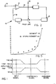
- This nonlinear digital to analog conversion effectively compresses the input analog signal amplitude range from 0 to Vref, as shown in Figure 1 of the accompanying drawings, which is a graphical representation of the companding action of a CVSD CODEC constructed in accordance with the invention.
- This compressed, digital signal is then transmitted to an expander, which converts the compressed signal to an expanded analog signal which is a good reproduction of the input analog signal.
- Syllabic filter 15 establishes the integrating voltage ("step size") used by encoder filter 17 used by the CODEC at any particular time during the analog-to-digital or digital-to-analog conversion process. Thus, if the output signal from encoder filter 17 does not "track" the input voltage fast enough, sylabbic filter 15 increases the step size.
- the output signals from comparator 12 and syllabic filter 15 are applied to polarity switch 16.
- Polarity switch 16 serves to provide either a positive or a negative voltage to encoder filter 17, depending on whether encoder filter must increase or decrease its output voltage in order to match the input signal Vin.
- the output signal from polarity switch 16 is applied to encoder filter 17, which serves to integrate the signals received from polarity switch 16 to provide an output signal which matches the input signal Vin.
- the output signal from encoder filter 17 is applied to the inverting input lead 18 of comparator 12.
- the delta modulated digital output signal representing the analog input signal applied to input terminal 11 is provided by the output signal bit stream from comparator 12 made available to other circuitry (not shown) on output terminal 21.
- the companding action provided by the circuit of Figure 2 improves the signal to noise performance of the CODEC, as compared with CODECs which utilize a fixed step size which is too great to accurately reproduce low level input signals Vin.
- the companding action provided by the circuit of Figure 2 also decreases the bit rate which is required by delta modulators which utilize a fixed step size which is sufficient small to allow proper reproduction of low level input signals Vin, but which is much smaller than the step size required to accurately reproduce large level input signals Vin.
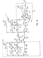
- Coincidence logic 14 receives an input signal on input terminal 21 from comparator 12 ( Figure 2 ). This input signal is clocked into four bit shift register 22. When the output signals AO through A3 provided by shift register 22 are all logical zeros or all logical ones, indicating that the output signal from encoder filter 17 ( Figure 2) has not tracked the input signal Vin and thus that the step size provided by syllabic filter 15 is too small, the output signal from OR gate 29 goes high, thereby connecting capacitor 26 to reference voltage Vref through resistor 25, thereby charging capacitor 26 and increasing the output voltage available on lead 27.
- This output voltage on lead 27 is applied to encoder filter 17 ( Figure 2), thereby increasing the step size.
- the output signal from comparator 12 ( Figure 2) toggles between one and zero and the output signals AO through A3 provided by shift register 22 are not all logical ones or zeros which cause the output signal from OR gate 29 to go low, thereby discharging capacitor 26 through resistor 25, thereby decreasing the voltage available on output terminal 27.
- This discrease in output voltage on terminal 27 causes the step size to decrease, providing more accurate conversion of the input signal.
- such a prior art syllabic filter 20 utilizing shift register 22 as coincidence logic has not proven adequate to provide sufficiently low distortion due to poor control of the step size.
- syllabic filter 15 has been satisfactorily realized in discrete form by cascading two very low frequency single pole sections, as shown in the schematic diagram of Figure 4.
- MOS Metal oxide silicon
- resistor values, capacitor values, and resistor ratios are not highly controllable.
- the syllabic filter shown on the schematic diagram of Figure 3 relies on the absolute values of resistors 35 and 37, and 39 and 41, and capacitors 38 and 42 to define the operating characteristics (such as time constants) of the syllabic filter.
- switched capacitor resistor equivalent technology has been developed, as described in an article by Allstot, et al., entitled “MOS Switched Capacitor Ladder Filters", IEEE Journal of Solid-State Circuits, Volume SC-13, No. 6, December, 1978, pages 806 to 814, which is hereby incorporated by reference.
- Switched capacitor resistor equivalent technology utilizes a capacitor and appropriate switches to form a resistor equivalent.
- the present invention provides a coder-decoder comprising an input terminal for receiving an input signal to be converted, a comparator for providing a binary digit output signal, the comparator having a first input lead connected to the input terminal, a second input lead, and an output lead, an encoder filter for providing an encoder filter output voltage, the encoder filter having an input lead, and an output lead connected to the second input lead of the comparator, and coincidence logic for providing a coincidence signal when the binary digit output signal from the comparator has been a logical one or a logical zero during each of the previous N sample periods, where N is a selected positive integer, characterized by:
- the present invention also provides a method of controlling the integration signal magnitude in a continuously variable slope delta coder-decoder (CVSD CODEC) comprising the steps of comparing the magnitudes of the input signal and the encoder filter signal and providing a comparator bit, storing the value of the comparator bit during the previous N sampling periods providing a coincidence signal when the value of the comparator bit during the previous N sampling periods are all logical ones or all logical zeros, characterised by the steps of:
- CVSD CODEC continuously variable slope delta coder-decoder
- This invention thus allows a unique CVSD CODEC to be provided utilizing switched capacitor technology.
- the syllabic filter included in this CVSD CODEC provides a large number of possible step sizes, thereby allowing the CVSD CODEC to accurately track and convert a wide range of input voltages.
- the coincidence logic of the CVSD CODEC of this invention determines how accurately the input voltage is being tracked, and the syllabic filter provides an appropriate step size based upon the output signals of the coincidence logic. Large step sizes are provided for converting input voltages having large magnitudes, and small step sizes are used to convert input voltages having small magnitudes, thereby providing the very accurate resolution of input voltages over the wide range of magnitudes, while minimizing the bit rate required.
- a syllabic filter 15 for use in a CVSD CODEC having a block diagram as in Figure 2, a syllabic filter 15 is provided, which, at any given time, generates a desired one of a plurality of possible step sizes, thereby allowing the output voltage of the encoder filter 17 to track the input voltage Vin applied to the CVSD modulator as accurately and as quickly as possible.
- Figure 5 depicts the plurality of step sizes that can be generated by such a syllabic filter in accordance with the invention. As shown in the graphical representation of Figure 5, the range of step sizes provided by such a syllabic filter is provided in a plurality of eight "segments", each segment providing a plurality of 16 step sizes. Accordingly, a total of 128 step sizes are available.
- coincidence logic 14 includes an N bit shift register 14-1 (where N is a selected positive integer), in one embodiment, a four bit shift register. Shift register 14-1 stores a plurality of bits provided on lead 13 from the output lead of voltage comparator 12 ( Figure 2 ) which define the relationship during the previous N sampling periods between the input voltage Vin applied to input terminal 11 and the output voltage Venc from encoder filter 17 available on lead 18.
- shift register 14-1 provides an indication of whether each of the past N samples of the output voltage Venc from encoder filter 14 is greater than or less than the past N samples of the input voltage Vin applied to input terminal 11, which is defined by the output sign bit provided by voltage comparator 12 on output terminal 21.
- the output sign bit from comparator 12 is a logical one.
- the output sign bit from comparator 12 is a logical zero.
- NOR gate 14-2 and AND gate 14-3, and OR gate 14-4 provide a logical zero signal on lead 14-4a when coincidence is achieved.
- NOR gate 14-2 With all zeros stored in shift register 14-1, NOR gate 14-2 provides a logical one output signal, thereby generating a logical one output signal on lead 14-4a.
- AND gate Conversely, when all ones are stored in shift register 14-1, AND gate provides a logical one output signal, which in turn cause a logical one to be generated by OR gate 14-4 on lead 14-4a.
- shift register 14-1 stores both logical zeros and ones
- NOR gate 14-2 and AND gate 14-3 provide logical zeros on their output leads
- OR gate 14-4 provides a logical zero output signal on lead 14-4a, thus indicating that coincidence has not been achieved.
- syllabic filter 15 provides a selected one of 128 voltages or "step sizes" to polarity switch 16, and polarity switch 16 applies either the positive or the negative of this output voltage of syllabic filter 15 to encoder filter 17.
- polarity switch 16 causes encoder filter 17 to integrate either the positive or the negative value of the output voltage from syllabic filter 15, depending on whether the output voltage from encoder filter 17 is less than or greater than, respectively, the input voltage Vin, as defined by the output sign bit from comparator 12.
- up/down 14-5 counter within syllabic filter 15 is caused to count up one count.
- up/down counter 14-5 is a seven bit up/down counter, thereby capable of counting from 0000000 to 1111111, or a total of 128 counts. During each sampling period when coincidence logic 14 indicates that coincidence is not achieved, seven bit up/down counter 14-5 decreases its count by one.
- the output voltage from syllabic filter 15 which is the magnitute of the step size by which encoder filter 17 will integrate, is increased, thereby causing encoder filter 17 to provide an output voltage Venc which is closer to the input voltage Vin.
- the count in seven bit up/down counter 14-5 is decreased, thereby causing the output voltage from syllabic filter 15 to decrease, which in turn causes the output voltage Venc from encoder filter 17 to more accurately track the input voltage Vin utilizing smaller voltage steps.
- coincidence logic 14 includes a rate multiplier, which causes count rate of shift register 14-1 to be increased as coincidence is approached.
- the count of the shift register 14-1 during each sampling period is not always equal to one, but rather is proportional to the count already stored in the shift register, thereby allowing the step size provided by the encoder filter to be adjusted more quickly to the value required for proper operation of the CVSD CODEC in response to the input signal Vin.
- the three most significant bits from seven bit up/down counter 14-5 determine which of the eight segments ( Figure 5) is to be utilized in generating the output voltage or "step size" provided by syllabic filter 15.
- the four least significant bits of up/down counter 14-5 are used to select which of the 16 steps of the selected segment is to be used.
- the three least significant bits provided by seven bit up/down counter 14-5 are applied to a well known three to eight decoder in order to provide output signals 0 ⁇ 0 through 0 ⁇ 7 , with signal 0 ⁇ 0 corresponding to the three least significant bits of up/down counter 14-5 equal to 000, and 0 ⁇ 7 corresponds to the three least significant bits of up/down counter 14-5 equal to 111.
- the four most significant bits from seven bit up/down counter 14-5 serve as signals ⁇ 8 through 0 ⁇ 11 , respectively.
- voltage comparator 12 is implemented in one embodiment as an operational amplifier 12-5 utilizing switched capacitor technology and MOS transistors serving as switches.
- clock signal 0 ⁇ 16 is high (logical "one) switches 12-2 and 12-4 are closed, and switch 12-1 is open.
- This causes the operational amplifier 12-5 to be placed in the unity gain mode, thus causing the inherent offset voltage Voff of operational amplifier 12-5 to be present on its inverting input lead, and thus on one plate of capacitor 12-3.
- the input voltage Vin is applied to the other plate of capacitor 12-3, thereby storing a voltage (Vin-Voff) on capacitor 12-3.
- 0 ⁇ 16 then goes low and y l7 goes high, thereby causing switches 12-2 and 12-4 to open and switch 12-1 to close.
- resistors RO through R14 are weighted in order to have the following resistance values:
- Switch 50-1 through 57-1 switches 50-1 through 57-1, and switches 51-2 through 57-2 are used to select desired taps on resistor ladder RO-R13, thereby providing reference voltages Vrl and Vr2, respectively.
- control signals 0 ⁇ 0 through 0 ⁇ 7 are provided by decoding the three last significant bits from up/down counter 14-5 ( Figure 6).
- resistor R14 has a resistance value of less than 127R, for example 32R. In this manner, the total resistance of the resistor ladder formed by resistors RO through R14 is equal to 160R. This causes the voltage at each tap of the resistor ladder to be greater than in the previous embodiment wherein resistor R16 has a resistance value of 127R, thereby allowing the use of a reference voltage Vref whose magnitude is less than the magnitude of the reference voltage Vref required in the previous embodiment, while maintaining the same voltages available on the taps of the resistor ladder formed by resistors RO through R14.
- Polarity switch 16 serves to select whether the selected voltages Vrl and Vr2 from the resistor ladder provided by resistors RO through R14 is inverted or not. Thus, for example, if it is desired to integrate on selected capacitors C8 through Cll the negative of the voltage Vrl provided by the appropriate tap on resistor ladder RO-R14, it is necessary to first integrate the ground voltage, and then integrate the selected voltage from the resistance ladder. This is done by making 0 ⁇ 14 high, and 0 ⁇ 15 low, thereby turning on switches 50a, 50b, 41a, 41b and turning off switches 51a and 51b.
- switch 52 turns on and switch 53 turns off, thereby causing ground voltage to be applied to input bus 99 of syllabic filter 15.
- switch 52 turns off and switch 53 turns on, thereby causing the selected voltage from resistor ladder RO through R13 to be applied to input bus 99 of syllabic filter 15.
- the negative of the voltage Vr2 is integrated on capacitor Cx through bus 199.
- Switched capacitor gain stage 15a serves to select the desired segment ( Figure 2).
- Figure 2 A more detailed description of the operation of a switched capacitor gain stage is described in co-pending United States Patent Application Serial No. 06/292,870, Filed August 14, 1981 on an invention of Haque, et al., which is assigned to American Microsystems, Inc., the assignee of this invention, and which is hereby incorporated by reference.
- the design of switched capacitor gain stages 60 and 70 which minimize the effect of the offset voltage of operational amplifiers is disclosed in U.S. Patent Application 06/287,387 filed July 27, 1981 and assigned to American Microsystems, Inc., and which is hereby incorporated by reference.
- the four most signficant bits from seven bit up/down counter 14-5 (Fig.6) of syllabic filter 15 serve to provide signals 0 ⁇ 8 through 0 ⁇ 11 , which in turn each select and control the operation of an associated one of capacitors C8 through Cll, respectively.
- Capacitors C8 through Cll have capacitance values of C, 2C, 4C, and 8C, respectively.
- Integrator capacitor 66 has a capacitance of C.
- Vout(a) the output voltage component of switched capacitor gain stage 15a due to Vrl;
- the output voltage Vout from switched capacitor gain stage 15a is equal to
- Switched capacitor gain stage 70 which is identical in operation with switched capacitor gain stage 60, serves to amplify the output signal Vout from switched capacitor gain stage 60 and provide an encoder filter output voltage Venc on output lead 18 of switched capacitor gain stage 70.
- This output voltage Venc is in turn applied to one input lead of comparator 12.
- Comparator 12 serves to provide an output signal on output terminal 21 indicating whether the input voltage Vin is greater than or less than the encoder filter output voltage Venc. As previously described, this output signal on terminal 21 is applied to coincidence logic 14 ( Figures 2 and 6) and polarity switch 16 ( Figures 2 and 7a), thereby providing proper operation of the CVSD CODEC constructed in accordance with this invention.
- capacitors C8 through Cll and CX serve both as the weighting capacitors to provide the appropriate step size, and the input capacitor of switched capacitor gain stage 60, thereby eliminating the need for an additional input capacitor and appropriate switches for sampling the input voltage applied to operational amplifier 61.
- the elimination of this extra input capacitor saves valuable area on an integrated circuit device, when the CVSD CODEC of this invention is formed as a monolithic integrated circuit.
- the elimination of the additional input capacitor and associated switches minimizes offset voltages, thereby making the CVSD CODEC of this invention more accurate.
Abstract
Description
- This invention relates to a coder-decoder (CODEC) and to a method of controlling the integration signal magnitude in a coder-decoder.
- Analog-to-digital converters convert an analog signal, typically an analog voltage, into a digital signal. This necessarily requires quantizing the range of analog signal into a number of discrete voltage ranges. For example, in one system a binary signal of 000 will be generated for all voltages ranging from 0 to 0.1 volts, a binary 001 signal will be generated for all voltages greater than 0.1 volt and not greater than 0.2 volts, etc.
- In some applications, this technique of utilizing voltage steps of a fixed size over the entire range of input voltages is adequate. However, in many instances, in particular in the digital-to-analog and analog-to-digital conversion of speech signals, for example in the operation of a coder-decoder, the use of a large step size will effectively preclude accurate conversion of low level signals, thereby providing unacceptable distortion of the signal. On the other hand, the use of a fixed step of small value, while preventing distortion of low level signals, results in a large number of discrete steps over the entire range of input signals, thereby requiring the digital word representing the analog signal to be rather large. The larger the word size, the greater the transmission rate required to transmit the digital representation of an analog signal.
- In order to minimize the transmission rate and yet provide a high quality output signal with little distortion, compressor/expanders (companders) are used. It has been found that rather large step sizes may be used when converting speech signals lying in the middle and high end of the speech signal amplitude range without causing excessive distortion of the speech signal. Accordingly, it is highly desirable to utilize a digital-to-analog or analog-to-digital conversion technique which does not use a plurality of steps of equal size, but which uses small steps for the conversion of low level signals, and larger steps for the conversion of larger signals. One technique for doing this is called the continuously variable slope delta (CVSD) modulator, which provides a plurality of steps, each step being of a different size. The smallest step is used to convert low level signals (i.e., those signals having amplitudes near 0 volts), and the steps increase in size, with the largest step being used to convert the largest signals (i.e., those signals having amplitudes of ± Vref, where Vref is the magnitude of the reference voltage used in the CVSD modulator). This nonlinear digital to analog conversion effectively compresses the input analog signal amplitude range from 0 to Vref, as shown in Figure 1 of the accompanying drawings, which is a graphical representation of the companding action of a CVSD CODEC constructed in accordance with the invention. This compressed, digital signal is then transmitted to an expander, which converts the compressed signal to an expanded analog signal which is a good reproduction of the input analog signal.
- One prior art circuit for generating the required step sizes used in a CVSD CODEC is shown in the block diagram of Figure 2 of the accompanying drawings. The analog input signal Vin to be converted is applied to the noninverting input lead 11 of
comparator 12. The output signal fromcomparator 12 is applied vialead 13 tocoincidence logic 14,Coincidence logic 14 serves to detect when the output signal fromcomparator 12 has been continuously either high or low for a plurality of samples, thus indicating that the output signal generated by encoder filter 17 (which is fully described later) is not accurately following the input signal. The output signal fromcoincidence logic 14 is applied tosyllabic filter 15.Syllabic filter 15 establishes the integrating voltage ("step size") used byencoder filter 17 used by the CODEC at any particular time during the analog-to-digital or digital-to-analog conversion process. Thus, if the output signal fromencoder filter 17 does not "track" the input voltage fast enough,sylabbic filter 15 increases the step size. The output signals fromcomparator 12 andsyllabic filter 15 are applied topolarity switch 16.Polarity switch 16 serves to provide either a positive or a negative voltage toencoder filter 17, depending on whether encoder filter must increase or decrease its output voltage in order to match the input signal Vin. The output signal frompolarity switch 16 is applied toencoder filter 17, which serves to integrate the signals received frompolarity switch 16 to provide an output signal which matches the input signal Vin. In turn, the output signal fromencoder filter 17 is applied to the invertinginput lead 18 ofcomparator 12. The delta modulated digital output signal representing the analog input signal applied to input terminal 11 is provided by the output signal bit stream fromcomparator 12 made available to other circuitry (not shown) onoutput terminal 21. - The companding action provided by the circuit of Figure 2 improves the signal to noise performance of the CODEC, as compared with CODECs which utilize a fixed step size which is too great to accurately reproduce low level input signals Vin. The companding action provided by the circuit of Figure 2 also decreases the bit rate which is required by delta modulators which utilize a fixed step size which is sufficient small to allow proper reproduction of low level input signals Vin, but which is much smaller than the step size required to accurately reproduce large level input signals Vin.
- One type of prior art
syllabic filter 20 is shown in the schematic diagram of Figure 3 together with one prior art circuit serving ascoincidence logic 14.Coincidence logic 14 receives an input signal oninput terminal 21 from comparator 12 (Figure 2). This input signal is clocked into fourbit shift register 22. When the output signals AO through A3 provided byshift register 22 are all logical zeros or all logical ones, indicating that the output signal from encoder filter 17 (Figure 2) has not tracked the input signal Vin and thus that the step size provided bysyllabic filter 15 is too small, the output signal fromOR gate 29 goes high, thereby connectingcapacitor 26 to reference voltage Vref throughresistor 25, thereby chargingcapacitor 26 and increasing the output voltage available on lead 27. This output voltage on lead 27 is applied to encoder filter 17 (Figure 2), thereby increasing the step size. Conversely, when the step size is too large, the output signal from comparator 12 (Figure 2) toggles between one and zero and the output signals AO through A3 provided byshift register 22 are not all logical ones or zeros which cause the output signal fromOR gate 29 to go low, thereby dischargingcapacitor 26 throughresistor 25, thereby decreasing the voltage available on output terminal 27. This discrease in output voltage on terminal 27 causes the step size to decrease, providing more accurate conversion of the input signal. However, such a prior artsyllabic filter 20 utilizingshift register 22 as coincidence logic has not proven adequate to provide sufficiently low distortion due to poor control of the step size. - In the prior art,
syllabic filter 15 has been satisfactorily realized in discrete form by cascading two very low frequency single pole sections, as shown in the schematic diagram of Figure 4. However, it is highly desirable to fabricate CODECs in integrated circuit form, thereby achieving substantial cost and size reductions over CODECs formed from discrete components. Metal oxide silicon (MOS) technology is especially useful to form very large integrated circuits, typically containing as many as five thousand transistors to form a complex circuit of which a CODEC is only a part. However, in MOS technology, resistor values, capacitor values, and resistor ratios are not highly controllable. The syllabic filter shown on the schematic diagram of Figure 3 relies on the absolute values ofresistors capacitors - However, implementation of the syllabic filter of Figure 4 as an MOS integrated circuit utilizing switched capacitor technology provides very poor performance due to the very long time constants involved. Due to the very long time constants, the capacitance value of the capacitors used to form switched
capacitor feedback resistors syllabic filter 15 must be less than one millivolt. DC offset voltages are caused by undesirable feedthrough of clock signals and offset voltages inherent in all operational amplifiers due to finite component mismatches. When implementing the syllabic filter of Figure 4 using switched comparator resistor equivalents, an offset voltage of approximately 100 millivolts was realized, thereby precluding use of this type of syllabic filter utilizing capacitor technology. - The present invention provides a coder-decoder comprising an input terminal for receiving an input signal to be converted, a comparator for providing a binary digit output signal, the comparator having a first input lead connected to the input terminal, a second input lead, and an output lead, an encoder filter for providing an encoder filter output voltage, the encoder filter having an input lead, and an output lead connected to the second input lead of the comparator, and coincidence logic for providing a coincidence signal when the binary digit output signal from the comparator has been a logical one or a logical zero during each of the previous N sample periods, where N is a selected positive integer, characterized by:
- a syllabic filter responsive to the coincidence logic, the syllabic filter providing a syllabic filter output signal having a magnitude proportional to the number of preceding sample periods in which the coincidence signal is present; and
- polarity switch means responsive to the binary digit output signal, the polarity switch means connecting the positive value of the syllabic filter output signal when the binary digit output signal is of a first binary value, and the negative value of the syllabic filter output signal when the binary digit output signal is of a second binary value opposite the first binary value.
- The present invention also provides a method of controlling the integration signal magnitude in a continuously variable slope delta coder-decoder (CVSD CODEC) comprising the steps of comparing the magnitudes of the input signal and the encoder filter signal and providing a comparator bit, storing the value of the comparator bit during the previous N sampling periods providing a coincidence signal when the value of the comparator bit during the previous N sampling periods are all logical ones or all logical zeros, characterised by the steps of:
- storing the coincidence signal from the previous N sampling periods; and
- generating an integration voltage proportional to the number of coincidence signals during the previous N sampling periods.
- This invention thus allows a unique CVSD CODEC to be provided utilizing switched capacitor technology. The syllabic filter included in this CVSD CODEC provides a large number of possible step sizes, thereby allowing the CVSD CODEC to accurately track and convert a wide range of input voltages. The coincidence logic of the CVSD CODEC of this invention determines how accurately the input voltage is being tracked, and the syllabic filter provides an appropriate step size based upon the output signals of the coincidence logic. Large step sizes are provided for converting input voltages having large magnitudes, and small step sizes are used to convert input voltages having small magnitudes, thereby providing the very accurate resolution of input voltages over the wide range of magnitudes, while minimizing the bit rate required.
- With further reference to the accompanying drawings:
- Figure 5 is a diagram showing the 128 step sizes of an embodiment of the invention;
- Figure 6 is a schematic diagram of the coincidence logic used in accordance with this invention; and
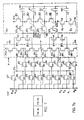
- Figure 7 is a diagram depicting how Figures 7a and 7b form a single schematic diagram of one CVSD CODEC constructed in accordance with this invention.
- In accordance with this invention, for use in a CVSD CODEC having a block diagram as in Figure 2, a
syllabic filter 15 is provided, which, at any given time, generates a desired one of a plurality of possible step sizes, thereby allowing the output voltage of theencoder filter 17 to track the input voltage Vin applied to the CVSD modulator as accurately and as quickly as possible. Figure 5 depicts the plurality of step sizes that can be generated by such a syllabic filter in accordance with the invention. As shown in the graphical representation of Figure 5, the range of step sizes provided by such a syllabic filter is provided in a plurality of eight "segments", each segment providing a plurality of 16 step sizes. Accordingly, a total of 128 step sizes are available. - A detailed schematic diagram of a
syllabic filter 15 in accordance with the invention is shown in Figures 6 and 7. Referring to Figures 2 and 6,coincidence logic 14 includes an N bit shift register 14-1 (where N is a selected positive integer), in one embodiment, a four bit shift register. Shift register 14-1 stores a plurality of bits provided onlead 13 from the output lead of voltage comparator 12 (Figure 2) which define the relationship during the previous N sampling periods between the input voltage Vin applied to input terminal 11 and the output voltage Venc fromencoder filter 17 available onlead 18. In other words, shift register 14-1 provides an indication of whether each of the past N samples of the output voltage Venc fromencoder filter 14 is greater than or less than the past N samples of the input voltage Vin applied to input terminal 11, which is defined by the output sign bit provided byvoltage comparator 12 onoutput terminal 21. When the output voltage Venc fromencoder filter 17 is less than the input voltage Vin, the output sign bit fromcomparator 12 is a logical one. Conversely, when the output voltage Venc fromencoder filter 17 is greater than the input voltage Vin applied to terminal 11, the output sign bit fromcomparator 12 is a logical zero. - "Coincidence" is defined, for the purposes of this application, as being when each of the plurality of bits stored in the shift register 14-1 of
coincidence logic 14, are of equal value. Thus, when a four bit shift register is used incoincidence logic 14, "coincidence" occurs when the four bit shift register 14-1 ofcoincidence logic 14 stores either four logical zeros, or four logical ones. When shift register 14-1 stores four logical zeros, it indicates that the output voltage fromencoder filter 17 is not tracking the input voltage applied to input terminal 11, and in fact the output voltage fromencoder filter 14 has been greater than the input voltage on terminal 11 for the past four sampling periods. Conversely, when the four bit shift register 14-1 ofcoincidence logic 14 stores four logical ones, this indicates that the output voltage fromencoder filter 17 is not tracking the input voltage applied to input terminal 11, and in fact that the output voltage fromencoder filter 17 has been less than the input voltage applied to terminal 11 during the past four sampling periods. - The logic circuitry provided by NOR gate 14-2 and AND gate 14-3, and OR gate 14-4 provide a logical zero signal on lead 14-4a when coincidence is achieved. With all zeros stored in shift register 14-1, NOR gate 14-2 provides a logical one output signal, thereby generating a logical one output signal on lead 14-4a. Conversely, when all ones are stored in shift register 14-1, AND gate provides a logical one output signal, which in turn cause a logical one to be generated by OR gate 14-4 on lead 14-4a. If shift register 14-1 stores both logical zeros and ones, NOR gate 14-2 and AND gate 14-3 provide logical zeros on their output leads, and OR gate 14-4 provides a logical zero output signal on lead 14-4a, thus indicating that coincidence has not been achieved. When coincidence is achieved, the encoder filter is not tracking the input voltage properly, and accordingly a voltage of greater amplitude must be provided by
syllabic filter 15 toencoder filter 17, thereby allowingencoder filter 17 to integrate this-voltage and thus cause the output voltage fromencoder filter 17 to more quickly move closer to the input voltage Vin, thereby causing the output voltage fromencoder filter 17 to better track the input voltage on terminal 11. As previously described,syllabic filter 15 provides a selected one of 128 voltages or "step sizes" topolarity switch 16, andpolarity switch 16 applies either the positive or the negative of this output voltage ofsyllabic filter 15 toencoder filter 17. Thus,polarity switch 16causes encoder filter 17 to integrate either the positive or the negative value of the output voltage fromsyllabic filter 15, depending on whether the output voltage fromencoder filter 17 is less than or greater than, respectively, the input voltage Vin, as defined by the output sign bit fromcomparator 12. - When
coincidence logic 14 indicates that coincidence has occurred (i.e., the shift register ofcoincidence logic 14 stores all logical zeros or all logical ones), an up/down 14-5 counter withinsyllabic filter 15 is caused to count up one count. In one embodiment of this invention, up/down counter 14-5 is a seven bit up/down counter, thereby capable of counting from 0000000 to 1111111, or a total of 128 counts. During each sampling period whencoincidence logic 14 indicates that coincidence is not achieved, seven bit up/down counter 14-5 decreases its count by one. As seven bit up/down counter 14-5 increases its count due to coincidence, the output voltage fromsyllabic filter 15, which is the magnitute of the step size by whichencoder filter 17 will integrate, is increased, thereby causingencoder filter 17 to provide an output voltage Venc which is closer to the input voltage Vin. Conversely, when coincidence is not detected bycoincidence logic 14, the count in seven bit up/down counter 14-5 is decreased, thereby causing the output voltage fromsyllabic filter 15 to decrease, which in turn causes the output voltage Venc fromencoder filter 17 to more accurately track the input voltage Vin utilizing smaller voltage steps. This is necessary because, when coincidence is not detected, the output voltage Venc fromencoder filter 17 has not been continuously either greater than or less than the input voltage Vin, and thus is doing a reasonable job in tracking the input voltage Vin. In one embodiment of this invention,coincidence logic 14 includes a rate multiplier, which causes count rate of shift register 14-1 to be increased as coincidence is approached. Thus, in this embodiment of the invention, the count of the shift register 14-1 during each sampling period is not always equal to one, but rather is proportional to the count already stored in the shift register, thereby allowing the step size provided by the encoder filter to be adjusted more quickly to the value required for proper operation of the CVSD CODEC in response to the input signal Vin. - The three most significant bits from seven bit up/down counter 14-5 determine which of the eight segments (Figure 5) is to be utilized in generating the output voltage or "step size" provided by
syllabic filter 15. The four least significant bits of up/down counter 14-5 are used to select which of the 16 steps of the selected segment is to be used. The three least significant bits provided by seven bit up/down counter 14-5 are applied to a well known three to eight decoder in order to provide output signals 0̸0 through 0̸7, with signal 0̸0 corresponding to the three least significant bits of up/down counter 14-5 equal to 000, and 0̸7 corresponds to the three least significant bits of up/down counter 14-5 equal to 111. The four most significant bits from seven bit up/down counter 14-5 serve as signals ø8 through 0̸11, respectively. - Referring now to Figure 7,
voltage comparator 12 is implemented in one embodiment as an operational amplifier 12-5 utilizing switched capacitor technology and MOS transistors serving as switches. When clock signal 0̸16 is high (logical "one") switches 12-2 and 12-4 are closed, and switch 12-1 is open. This causes the operational amplifier 12-5 to be placed in the unity gain mode, thus causing the inherent offset voltage Voff of operational amplifier 12-5 to be present on its inverting input lead, and thus on one plate of capacitor 12-3. The input voltage Vin is applied to the other plate of capacitor 12-3, thereby storing a voltage (Vin-Voff) on capacitor 12-3. 0̸16 then goes low and yl7 goes high, thereby causing switches 12-2 and 12-4 to open and switch 12-1 to close. This causes the output voltage Venc fromencoder filter 17 to be applied to one plate of capacitor 12-3, thereby causing capacitor 12-3 to store a voltage equal to (Venc - Voff) - (Vin - Voff) = (Venc - Vin). The output voltage onoutput terminal 21 is thus either a logical one or a logical zero, depending on whether the output voltage Venc fromencoder filter 17 is less than or greater than, respectively, the input voltage Vin. As previously described in conjunction with Figure 2, this output voltage fromcomparator 12 serves to controlpolarity switch 16 andcoincidence logic 14. - A resistance ladder formed of resistors RO through R14 having a plurality of taps located therebetween allows a desired tap to be selected and thus a voltage between Vref and ground to be used to select which step within the selected segment is to be utilized. The operation of the circuit of Figure 7a to select the desired segment will be fully described later. In one embodiment of this invention, resistors RO through R14 are weighted in order to have the following resistance values:

- Two banks of switches (i.e., switches 50-1 through 57-1, and switches 51-2 through 57-2 are used to select desired taps on resistor ladder RO-R13, thereby providing reference voltages Vrl and Vr2, respectively. As previously described, control signals 0̸0 through 0̸7 are provided by decoding the three last significant bits from up/down counter 14-5 (Figure 6).
- When 0̸0 is high, 0̸1 through ø7 are all low, and thus the voltage provided by the tap between resistors RO and ground is selected as voltage Vrl. Based on the resistance ratios previously described, the voltage on this tap is equal to Vref (R/255R) = Vref/255. Similarly, when 0̸1 is high and 00, 0̸2 through ø7 are low, the tap between resistors Rl and R2 selected for Vrl, thereby providing a voltage equal to Vref (2R/255R) = 2Vref/255, and the tap between resistors RO and ground selected for Vr2, thereby providing a voltage Vr2 equal to Vref/255. In this manner, the-appropriate voltages Vrl and Vr2 which determine the step within the selected segment are selected.
- In another embodiment of this invention, resistor R14 has a resistance value of less than 127R, for example 32R. In this manner, the total resistance of the resistor ladder formed by resistors RO through R14 is equal to 160R. This causes the voltage at each tap of the resistor ladder to be greater than in the previous embodiment wherein resistor R16 has a resistance value of 127R, thereby allowing the use of a reference voltage Vref whose magnitude is less than the magnitude of the reference voltage Vref required in the previous embodiment, while maintaining the same voltages available on the taps of the resistor ladder formed by resistors RO through R14.
-
Polarity switch 16 serves to select whether the selected voltages Vrl and Vr2 from the resistor ladder provided by resistors RO through R14 is inverted or not. Thus, for example, if it is desired to integrate on selected capacitors C8 through Cll the negative of the voltage Vrl provided by the appropriate tap on resistor ladder RO-R14, it is necessary to first integrate the ground voltage, and then integrate the selected voltage from the resistance ladder. This is done by making 0̸14 high, and 0̸15 low, thereby turning onswitches 50a, 50b, 41a, 41b and turning off switches 51a and 51b. Then, when 0̸13 goes high and 0̸13 goes low,switch 52 turns on and switch 53 turns off, thereby causing ground voltage to be applied to inputbus 99 ofsyllabic filter 15. Then, when 0̸13 goes low and 0̸13 goes high,switch 52 turns off and switch 53 turns on, thereby causing the selected voltage from resistor ladder RO through R13 to be applied to inputbus 99 ofsyllabic filter 15. Similarly, the negative of the voltage Vr2 is integrated on capacitor Cx throughbus 199. - Conversely, when it is desired to integrate on selected capacitors C8 through Cll the positive of the voltage Vrl, it is necessary to first sample the voltage Vrl and then integrate the ground voltage. Ø14 is placed low and 0̸15 is placed high, thereby turning off
switches 50a and 50b and turning on switches 51a and 51b. Thus, when 0̸13 goes high,switch 52 turns on and switch 53 turns off, thereby applying the selected voltage from resistor ladder RO through R13 to theinput bus 99 ofsyllabic filter 14. Then, when yl3 goes low and 0̸13 goes high,switch 52 turns off and switch 53 turns on, thereby applying the ground voltage to theinput bus 99 ofsyllabic filter 15, as desired. - Switched capacitor gain stage 15a serves to select the desired segment (Figure 2). A more detailed description of the operation of a switched capacitor gain stage is described in co-pending United States Patent Application Serial No. 06/292,870, Filed August 14, 1981 on an invention of Haque, et al., which is assigned to American Microsystems, Inc., the assignee of this invention, and which is hereby incorporated by reference. The design of switched capacitor gain stages 60 and 70 which minimize the effect of the offset voltage of operational amplifiers is disclosed in
U.S. Patent Application 06/287,387 filed July 27, 1981 and assigned to American Microsystems, Inc., and which is hereby incorporated by reference. - The four most signficant bits from seven bit up/down counter 14-5 (Fig.6) of
syllabic filter 15 serve to provide signals 0̸8 through 0̸11, which in turn each select and control the operation of an associated one of capacitors C8 through Cll, respectively. Capacitors C8 through Cll have capacitance values of C, 2C, 4C, and 8C, respectively. Integrator capacitor 66 has a capacitance of C. Thus, the output voltage Vout of switched capacitor gain stage 15a, ignoring the effect of capacitor CX, is defined as:
- Vrl = the input voltage provided by switches 50-1 through 57-1 and resistor ladder RO-R14;
- CT = the total capacitance of selected capacitors C8 through Cll;
- K2C - the capacitance of capacitor 66; and
- h - 1, if polarity switch 16 causes the positive of voltage Vrl to be integrated by selected capacitors C8 through Cll and h = 2 if polarity switch 16 causes the negative of voltage Vrl to be integrated by selected capacitors C8 through Cll.
- Capacitor CX, having
capacitance value 16C, andpolarity switch 16b, switches 47 and 48, and switches 51-2 through 57-2, contribute to the output voltage Vout fromoperational amplifier 61 is defined as follows:
- Vr2 = The input voltage provided by switches 51-2 through 57-2 and resistor ladder R0-R14;
- 16C = the capacitance of capacitor Cx;
- h - 1, if polarity switch causes the positive of voltage Vr2 to be integrated by capacitor Cx and h2 if polarity switch 16 causes the negative of voltage Vr2 to be integrated by capacitor Cx.
- The output voltage Vout from switched capacitor gain stage 15a is equal to

- Switched
capacitor gain stage 70, which is identical in operation with switchedcapacitor gain stage 60, serves to amplify the output signal Vout from switchedcapacitor gain stage 60 and provide an encoder filter output voltage Venc onoutput lead 18 of switchedcapacitor gain stage 70. This output voltage Venc is in turn applied to one input lead ofcomparator 12.Comparator 12 serves to provide an output signal onoutput terminal 21 indicating whether the input voltage Vin is greater than or less than the encoder filter output voltage Venc. As previously described, this output signal onterminal 21 is applied to coincidence logic 14 (Figures 2 and 6) and polarity switch 16 (Figures 2 and 7a), thereby providing proper operation of the CVSD CODEC constructed in accordance with this invention. - In accordance with this invention, capacitors C8 through Cll and CX serve both as the weighting capacitors to provide the appropriate step size, and the input capacitor of switched
capacitor gain stage 60, thereby eliminating the need for an additional input capacitor and appropriate switches for sampling the input voltage applied tooperational amplifier 61. The elimination of this extra input capacitor saves valuable area on an integrated circuit device, when the CVSD CODEC of this invention is formed as a monolithic integrated circuit. Furthermore, the elimination of the additional input capacitor and associated switches minimizes offset voltages, thereby making the CVSD CODEC of this invention more accurate. - The specific embodiments of this invention described in this specification are intended to serve by way of example and are not a limitation on the scope of the invention. Numerous other embodiments of this invention will become apparent to those of ordinary skill in the art in light of the teachings of this specification.
Claims (4)
Priority Applications (1)
| Application Number | Priority Date | Filing Date | Title |
|---|---|---|---|
| AT84300824T ATE73971T1 (en) | 1983-02-22 | 1984-02-09 | ENCODER-DECODER AND CONTROL OF THE SAME. |
Applications Claiming Priority (2)
| Application Number | Priority Date | Filing Date | Title |
|---|---|---|---|
| US468608 | 1983-02-22 | ||
| US06/468,608 US4541103A (en) | 1983-02-22 | 1983-02-22 | Digitally controlled syllabic filter for a delta modulator |
Publications (3)
| Publication Number | Publication Date |
|---|---|
| EP0119716A2 true EP0119716A2 (en) | 1984-09-26 |
| EP0119716A3 EP0119716A3 (en) | 1987-09-09 |
| EP0119716B1 EP0119716B1 (en) | 1992-03-18 |
Family
ID=23860499
Family Applications (1)
| Application Number | Title | Priority Date | Filing Date |
|---|---|---|---|
| EP84300824A Expired - Lifetime EP0119716B1 (en) | 1983-02-22 | 1984-02-09 | Coder-decoder and control thereof |
Country Status (6)
| Country | Link |
|---|---|
| US (1) | US4541103A (en) |
| EP (1) | EP0119716B1 (en) |
| JP (1) | JPS59161120A (en) |
| AT (1) | ATE73971T1 (en) |
| CA (1) | CA1230425A (en) |
| DE (2) | DE119716T1 (en) |
Families Citing this family (2)
| Publication number | Priority date | Publication date | Assignee | Title |
|---|---|---|---|---|
| JPH05268090A (en) * | 1992-03-17 | 1993-10-15 | Mitsubishi Electric Corp | Resistance ladder for decoding system |
| US5727023A (en) * | 1992-10-27 | 1998-03-10 | Ericsson Inc. | Apparatus for and method of speech digitizing |
Citations (1)
| Publication number | Priority date | Publication date | Assignee | Title |
|---|---|---|---|---|
| US4352191A (en) * | 1980-05-19 | 1982-09-28 | Un Chong K | Hybrid companding delta modulation system |
Family Cites Families (11)
| Publication number | Priority date | Publication date | Assignee | Title |
|---|---|---|---|---|
| US3784922A (en) * | 1971-06-22 | 1974-01-08 | Bell Telephone Labor Inc | Adaptive delta modulation decoder |
| JPS557970B2 (en) * | 1973-01-22 | 1980-02-29 | ||
| US3857111A (en) * | 1973-03-20 | 1974-12-24 | Univ Sherbrooke | Syllabic adaptative delta modulation system |
| US4035724A (en) * | 1974-05-08 | 1977-07-12 | Universite De Sherbrooke | Digital converter from continuous variable slope delta modulation to pulse code modulation |
| US4044306A (en) * | 1974-07-26 | 1977-08-23 | Universite De Snerbrooke | Digital converter from pulse code modulation to continuous variable slope delta modulation |
| JPS5414145A (en) * | 1977-07-04 | 1979-02-02 | Nippon Telegr & Teleph Corp <Ntt> | Polygonal line decoder of digital type |
| JPS6038058B2 (en) * | 1980-03-19 | 1985-08-29 | 松下電器産業株式会社 | Constant difference modulation method |
| DE3044765A1 (en) * | 1980-11-27 | 1982-07-08 | Siemens AG, 1000 Berlin und 8000 München | DIFFERENCE DIGITAL MODULATION OR -DEMODULATION SYSTEM WITH SIGNAL-DEPENDENT SCAN |
| US4446565A (en) * | 1980-12-30 | 1984-05-01 | Motorola, Inc. | CVSD Transmission with improved intelligibility of voice signals |
| JPS57116422A (en) * | 1981-01-09 | 1982-07-20 | Toshiba Corp | Analog waveform modulating and demodulating circuit |
| US4411002A (en) * | 1981-09-29 | 1983-10-18 | Magnavox Government And Industrial Electronics Company | Method and apparatus for a continuously variable slope delta range extender |
-
1983
- 1983-02-22 US US06/468,608 patent/US4541103A/en not_active Expired - Lifetime
-
1984
- 1984-02-09 DE DE198484300824T patent/DE119716T1/en active Pending
- 1984-02-09 DE DE8484300824T patent/DE3485583D1/en not_active Expired - Lifetime
- 1984-02-09 AT AT84300824T patent/ATE73971T1/en not_active IP Right Cessation
- 1984-02-09 EP EP84300824A patent/EP0119716B1/en not_active Expired - Lifetime
- 1984-02-21 CA CA000447895A patent/CA1230425A/en not_active Expired
- 1984-02-21 JP JP59031323A patent/JPS59161120A/en active Granted
Patent Citations (1)
| Publication number | Priority date | Publication date | Assignee | Title |
|---|---|---|---|---|
| US4352191A (en) * | 1980-05-19 | 1982-09-28 | Un Chong K | Hybrid companding delta modulation system |
Non-Patent Citations (2)
| Title |
|---|
| ICASSP '82 PROCEEDINGS - IEEE INTERNATIONAL CONFERENCE ON ACOUSTICS, SPEECH AND SIGNAL PROCESSING, Paris, 3rd - 5th May 1982, vol. 2, pages 980-983, Sponsored by IEEE, Acoustics, Speech and Signal Processing Society, New York, US; N. OHTA et al.: "A high quality ADM LSI CODEC at 32 KBIT/S for digital speech communications" * |
| IEEE JOURNAL OF SOLID-STATE CIRCUITS, vol. SC-18, no. 1, Feburary 1983, pages 33-39, IEEE, New York, US; K. IRIE et al.: "A single-chip ADM LSI CODEC" * |
Also Published As
| Publication number | Publication date |
|---|---|
| JPS59161120A (en) | 1984-09-11 |
| DE3485583D1 (en) | 1992-04-23 |
| JPH0444850B2 (en) | 1992-07-23 |
| EP0119716B1 (en) | 1992-03-18 |
| EP0119716A3 (en) | 1987-09-09 |
| CA1230425A (en) | 1987-12-15 |
| DE119716T1 (en) | 1985-08-14 |
| US4541103A (en) | 1985-09-10 |
| ATE73971T1 (en) | 1992-04-15 |
Similar Documents
| Publication | Publication Date | Title |
|---|---|---|
| US5006854A (en) | Method and apparatus for converting A/D nonlinearities to random noise | |
| US6255974B1 (en) | Programmable dynamic range sigma delta A/D converter | |
| US4385286A (en) | Use of single reference voltage for analog to digital or digital to analog conversion of bipolar signals | |
| US4638303A (en) | Digital-analog converter | |
| EP1317068B1 (en) | Incremental-delta analogue to digital conversion | |
| JPH11261764A (en) | Variable gain amplifier | |
| US5541599A (en) | Data independent loading of a reference in a discrete time system | |
| JPS6165626A (en) | A/d converter | |
| US4390844A (en) | Integration filter for step waveforms | |
| US5248974A (en) | Dielectric relaxation correction circuit for charge-redistribution a/d converters | |
| US4812817A (en) | Differential analog-digital converter with switched capacitors | |
| EP0536198A1 (en) | Process for the conversion of digital codes and digital-to-analog converter employing this process. | |
| EP0119716B1 (en) | Coder-decoder and control thereof | |
| US4451820A (en) | Charge redistribution integratable D/A convertor | |
| US4468654A (en) | Charge redistribution a-law PCM decoder | |
| US4573033A (en) | Filter circuit for digital-to-analog converter | |
| EP0035019A1 (en) | Cyclic digital-to-analog conversion system | |
| JPS61177819A (en) | Oversampling type digital/analog converter | |
| US4468653A (en) | Charge redistribution mu-law PCM decoder | |
| US5699064A (en) | Oversampling D/A converter using a bidirectional shift register | |
| KR0147489B1 (en) | Voltage gain amplifier converting single input into differential output | |
| Tsividis et al. | An all-MOS companded PCM voice encoder | |
| JPH0523650B2 (en) | ||
| KR930002129B1 (en) | Automatic linear compression circuit | |
| Hester et al. | A monolithic data acquisition channel |
Legal Events
| Date | Code | Title | Description |
|---|---|---|---|
| PUAI | Public reference made under article 153(3) epc to a published international application that has entered the european phase |
Free format text: ORIGINAL CODE: 0009012 |
|
| AK | Designated contracting states |
Designated state(s): AT DE FR GB IT NL SE |
|
| ITCL | It: translation for ep claims filed |
Representative=s name: DE DOMINICIS & PARTNERS |
|
| TCNL | Nl: translation of patent claims filed | ||
| EL | Fr: translation of claims filed | ||
| 17P | Request for examination filed |
Effective date: 19841220 |
|
| TCAT | At: translation of patent claims filed | ||
| DET | De: translation of patent claims | ||
| PUAL | Search report despatched |
Free format text: ORIGINAL CODE: 0009013 |
|
| AK | Designated contracting states |
Kind code of ref document: A3 Designated state(s): AT DE FR GB IT NL SE |
|
| 17Q | First examination report despatched |
Effective date: 19890628 |
|
| GRAA | (expected) grant |
Free format text: ORIGINAL CODE: 0009210 |
|
| AK | Designated contracting states |
Kind code of ref document: B1 Designated state(s): AT DE FR GB IT NL SE |
|
| PG25 | Lapsed in a contracting state [announced via postgrant information from national office to epo] |
Ref country code: SE Effective date: 19920318 Ref country code: IT Free format text: LAPSE BECAUSE OF FAILURE TO SUBMIT A TRANSLATION OF THE DESCRIPTION OR TO PAY THE FEE WITHIN THE PRESCRIBED TIME-LIMIT;WARNING: LAPSES OF ITALIAN PATENTS WITH EFFECTIVE DATE BEFORE 2007 MAY HAVE OCCURRED AT ANY TIME BEFORE 2007. THE CORRECT EFFECTIVE DATE MAY BE DIFFERENT FROM THE ONE RECORDED. Effective date: 19920318 |
|
| REF | Corresponds to: |
Ref document number: 73971 Country of ref document: AT Date of ref document: 19920415 Kind code of ref document: T |
|
| REF | Corresponds to: |
Ref document number: 3485583 Country of ref document: DE Date of ref document: 19920423 |
|
| EN | Fr: translation not filed | ||
| PG25 | Lapsed in a contracting state [announced via postgrant information from national office to epo] |
Ref country code: FR Effective date: 19920807 |
|
| PLBE | No opposition filed within time limit |
Free format text: ORIGINAL CODE: 0009261 |
|
| STAA | Information on the status of an ep patent application or granted ep patent |
Free format text: STATUS: NO OPPOSITION FILED WITHIN TIME LIMIT |
|
| 26N | No opposition filed | ||
| REG | Reference to a national code |
Ref country code: FR Ref legal event code: ST |
|
| NLS | Nl: assignments of ep-patents |
Owner name: AMI SPINCO INC., A DELAWARE CORPORATION;AMERICAN M |
|
| NLS | Nl: assignments of ep-patents |
Owner name: AMI SEMICONDUCTOR, INC. |
|
| REG | Reference to a national code |
Ref country code: GB Ref legal event code: IF02 |
|
| PGFP | Annual fee paid to national office [announced via postgrant information from national office to epo] |
Ref country code: NL Payment date: 20030121 Year of fee payment: 20 Ref country code: AT Payment date: 20030121 Year of fee payment: 20 |
|
| PGFP | Annual fee paid to national office [announced via postgrant information from national office to epo] |
Ref country code: GB Payment date: 20030205 Year of fee payment: 20 |
|
| PGFP | Annual fee paid to national office [announced via postgrant information from national office to epo] |
Ref country code: DE Payment date: 20030228 Year of fee payment: 20 |
|
| PG25 | Lapsed in a contracting state [announced via postgrant information from national office to epo] |
Ref country code: GB Free format text: LAPSE BECAUSE OF EXPIRATION OF PROTECTION Effective date: 20040208 |
|
| PG25 | Lapsed in a contracting state [announced via postgrant information from national office to epo] |
Ref country code: NL Free format text: LAPSE BECAUSE OF EXPIRATION OF PROTECTION Effective date: 20040209 Ref country code: AT Free format text: LAPSE BECAUSE OF EXPIRATION OF PROTECTION Effective date: 20040209 |
|
| REG | Reference to a national code |
Ref country code: GB Ref legal event code: PE20 |
|
| NLV7 | Nl: ceased due to reaching the maximum lifetime of a patent |
Effective date: 20040209 |