EP0118605A2 - Feedback circuit for a semiconductor active element sensor - Google Patents
Feedback circuit for a semiconductor active element sensor Download PDFInfo
- Publication number
- EP0118605A2 EP0118605A2 EP83111718A EP83111718A EP0118605A2 EP 0118605 A2 EP0118605 A2 EP 0118605A2 EP 83111718 A EP83111718 A EP 83111718A EP 83111718 A EP83111718 A EP 83111718A EP 0118605 A2 EP0118605 A2 EP 0118605A2
- Authority
- EP
- European Patent Office
- Prior art keywords
- fet
- semiconductor sensor
- sensor according
- gate
- change
- Prior art date
- Legal status (The legal status is an assumption and is not a legal conclusion. Google has not performed a legal analysis and makes no representation as to the accuracy of the status listed.)
- Granted
Links
Images


Classifications
-
- G—PHYSICS
- G01—MEASURING; TESTING
- G01L—MEASURING FORCE, STRESS, TORQUE, WORK, MECHANICAL POWER, MECHANICAL EFFICIENCY, OR FLUID PRESSURE
- G01L1/00—Measuring force or stress, in general
- G01L1/18—Measuring force or stress, in general using properties of piezo-resistive materials, i.e. materials of which the ohmic resistance varies according to changes in magnitude or direction of force applied to the material
-
- G—PHYSICS
- G01—MEASURING; TESTING
- G01D—MEASURING NOT SPECIALLY ADAPTED FOR A SPECIFIC VARIABLE; ARRANGEMENTS FOR MEASURING TWO OR MORE VARIABLES NOT COVERED IN A SINGLE OTHER SUBCLASS; TARIFF METERING APPARATUS; MEASURING OR TESTING NOT OTHERWISE PROVIDED FOR
- G01D5/00—Mechanical means for transferring the output of a sensing member; Means for converting the output of a sensing member to another variable where the form or nature of the sensing member does not constrain the means for converting; Transducers not specially adapted for a specific variable
- G01D5/12—Mechanical means for transferring the output of a sensing member; Means for converting the output of a sensing member to another variable where the form or nature of the sensing member does not constrain the means for converting; Transducers not specially adapted for a specific variable using electric or magnetic means
- G01D5/14—Mechanical means for transferring the output of a sensing member; Means for converting the output of a sensing member to another variable where the form or nature of the sensing member does not constrain the means for converting; Transducers not specially adapted for a specific variable using electric or magnetic means influencing the magnitude of a current or voltage
- G01D5/18—Mechanical means for transferring the output of a sensing member; Means for converting the output of a sensing member to another variable where the form or nature of the sensing member does not constrain the means for converting; Transducers not specially adapted for a specific variable using electric or magnetic means influencing the magnitude of a current or voltage by varying effective impedance of discharge tubes or semiconductor devices
- G01D5/183—Sensing rotation or linear movement using strain, force or pressure sensors
- G01D5/185—Sensing rotation or linear movement using strain, force or pressure sensors using piezoelectric sensors
-
- G—PHYSICS
- G01—MEASURING; TESTING
- G01L—MEASURING FORCE, STRESS, TORQUE, WORK, MECHANICAL POWER, MECHANICAL EFFICIENCY, OR FLUID PRESSURE
- G01L9/00—Measuring steady of quasi-steady pressure of fluid or fluent solid material by electric or magnetic pressure-sensitive elements; Transmitting or indicating the displacement of mechanical pressure-sensitive elements, used to measure the steady or quasi-steady pressure of a fluid or fluent solid material, by electric or magnetic means
- G01L9/0098—Measuring steady of quasi-steady pressure of fluid or fluent solid material by electric or magnetic pressure-sensitive elements; Transmitting or indicating the displacement of mechanical pressure-sensitive elements, used to measure the steady or quasi-steady pressure of a fluid or fluent solid material, by electric or magnetic means using semiconductor body comprising at least one PN junction as detecting element
-
- G—PHYSICS
- G01—MEASURING; TESTING
- G01L—MEASURING FORCE, STRESS, TORQUE, WORK, MECHANICAL POWER, MECHANICAL EFFICIENCY, OR FLUID PRESSURE
- G01L9/00—Measuring steady of quasi-steady pressure of fluid or fluent solid material by electric or magnetic pressure-sensitive elements; Transmitting or indicating the displacement of mechanical pressure-sensitive elements, used to measure the steady or quasi-steady pressure of a fluid or fluent solid material, by electric or magnetic means
- G01L9/02—Measuring steady of quasi-steady pressure of fluid or fluent solid material by electric or magnetic pressure-sensitive elements; Transmitting or indicating the displacement of mechanical pressure-sensitive elements, used to measure the steady or quasi-steady pressure of a fluid or fluent solid material, by electric or magnetic means by making use of variations in ohmic resistance, e.g. of potentiometers, electric circuits therefor, e.g. bridges, amplifiers or signal conditioning
- G01L9/06—Measuring steady of quasi-steady pressure of fluid or fluent solid material by electric or magnetic pressure-sensitive elements; Transmitting or indicating the displacement of mechanical pressure-sensitive elements, used to measure the steady or quasi-steady pressure of a fluid or fluent solid material, by electric or magnetic means by making use of variations in ohmic resistance, e.g. of potentiometers, electric circuits therefor, e.g. bridges, amplifiers or signal conditioning of piezo-resistive devices
Definitions
- the present invention relates to a semiconductor sensor and in particular to a semiconductor sensor having a voltage-controlled semiconductor active element.
- a pressure or strain sensor comprising an insulated-gate (IG or MOS) active element and utilizing the piezoresistive effect is proposed in Solid State Electronics, vol. 18, 1975, p.p. 295 to 299. That paper discloses a bridge circuit comprising four metal-oxide-semiconductor field- effect-transistors (MOS FET's), a differential amplifier comprising two MOS FET's and so on.
- MOS FET's metal-oxide-semiconductor field- effect-transistors
- a strain gauge comprising a bridge circuit composed of four IG FET's is proposed in Japanese Patent Application Laid-Open No. 7699/80 which corresponds to U.S. Patent Application Serial No. 920,137 filed on June 28, 1978.
- An object of the present invention is to provide a stable and highly sensitive semiconductor active element sensor having a negative feedback loop.
- the semiconductor active element may be formed by an insulated-gate field effect transistor (IG FET) having a channel structure responsive to a physical quantity to be measured.
- IG FET insulated-gate field effect transistor
- the drain voltage of the IG FET is negatively fed back to the gate thereof to let flow a nearly constant drain current through the IG FET.
- the stabilized drain current eliminates charging and discharging of the stray capacitance existing in the main current path, facilitating fast operation. Because of the stabilized drain current, the bias condition of the IG FET, and hence the power dissipation of the sensor are also stabilized. Therefore, the quantity of generated heat and hence the characteristics of the sensor are thermally stabilized.
- Another object of the present invention is to provide a semiconductor active element sensor comprising an insulated-gate field effect transistor (IG FET), a first amplifying means which is connected between the drain of the IG FET and the output terminal and has an amplification factor larger than unity, and a second amplifying means which is connected between the output terminal and the gate of the IG FET.
- the amplification factor of the first amplifying means is increased to provide a large output voltage.
- the amplification factor of the second amplifying means is adjusted to feed a stable bias to the gate of the IG FET.
- a capacitor for coupling the gate of the IG FET, to the source thereof may be placed in the second amplifying means so that a stable DC bias may be applied to the gate of the IG FET and the AC change in a physical quantity to be meansured may also be detected with high fidelity.
- a fixed load impedance Z L and a voltage amplifying circuit A 1 are connected to a drain D 1 terminal 1 of a MOS FET T l .
- the power supply voltage Vcc from the power source circuit PS is applied to the load impendance Z L .
- the gate G 1 of the MOS FET T 1 as well as the output terminal V are connected to the output 2 of the amplifying circuit A 1 .
- the source terminal S 1 of the MOS FET T 1 is connected to the ground.
- the voltage gain of the amplifying circuit A 1 is p.
- the MOS FET T 1 i.e. the channel thereof, has a pressure sensitive amplifying function.
- the feedback quantity of the gate bias is decreased.
- the feedback quantity is stabilized at a point where the difference between the change in the drain current caused by the pressure and the change in the drain current caused by the negative feedback balances with the resultant gate bias.
- Fig. 2 shows an example of relationship between the drain current I ds of a MOS FET illustrated in Fig. 1 and the gate voltage Vg s thereof. It is assumed that a MOS FET has an enhancement mode n-channel and is subjected to a compressive stress in parallel with the channel direction. It corresponds to the tensile stress in parallel with a p-channel. Upon application of pressure, a characteristic curve A corresponding to zero applied stress is replaced by a curve B. If the pressure is applied with the constant gate voltage, a point P on the curve A corresponding to a current value I do moves to a point R on the curve B, exhibiting the quantity of change
- the change in the drain current is transformed into the change in the drain voltage.
- the change in the drain voltage is amplified and negatively fed back to the gate G 1 of the MOS FET T 1 . That is to say, the gate voltage is changed so as to cancel the change in the drain current. If the voltage gain p is infinitely high, the change in the drain current will be completely canceled.
- the operation point R To restore the drain current to its original value I do by changing the gate voltage, the operation point R must be moved to a point Q along the line B. At this time, the gate voltage changes from V g (o) to V (p).
- the drain current of a MOS FET as a function of the gate voltage thereof is plotted for various temperatures under an identical pressure.
- the carrier mobility is decreased to decrease the drain current I ds according as the temperature is raised.
- the drain current I ds increases due to the reduced energy gap (red shift) and increase of thermally excited carriers.
- the MOS FET with no stress being applied thereto is biased to a point where the minimum variation in characteristics due to the temperature is caused, the variation in characteristics such as the thermal drift due to the temperature may be substantially made zero at least in the strainless state.
- Fig. 4 shows another embodiment of the present invention. This embodiment has an advantage that desired magnitude of output voltage may be obtained irrespective of the negative feedback quantity to the gate.
- a first amplifier A 1 having an amplification ratio ⁇ and a second amplifier N 1 are connected between the drain terminal D 1 of the MOS FET T 1 and the gate terminal G 1 thereof.
- the second or the negative feedback amplifier N 1 has a voltage gain of ⁇ which is usually less than unity.
- the amplifier N 1 may be constituted by using stable passive elements such as resistors and capacitors.
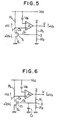
- Fig. 5 shows an example of the circuit illustrated in Fig. 4.
- the power supply voltage Vcc is fed to the drain terminal D 1 of the MOS FET T 1 through a resistor R L .
- the source terminal S 1 of the MOS FET T 1 is grounded.
- the noninverting input (+) of an operational amplifier A 1 is connected to the drain terminal D 1 of the MOS FET T 1 .
- a reference voltage source V B is connected to the inverting input (-) of the operational amplifier A 1 .
- the reference voltage source may be formed by a voltage divider circuit composed of diffusion resistors.
- An output terminal V for the detected value and a resistor R 1 are connected to the output terminal 2 of the operational amplifier A 1 .
- the gate terminal G 1 of the MOS FET T 1 is connected to the other terminal 3 of the resistor R 1 .
- the operational amplifier A 1 in this example corresponds to the first amplifier A 1 illustrated in Fig. 4.
- the voltage divider circuit composed of resistors R 1 and R 2 corresponds to the second amplifier N 1 illustrated in Fig. 4.
- the resistors R 1 and R 2 may be formed by using diffusion resistors or polysilicon resistors on the same semiconductor chip as that of the MOS FET.
- the voltage V 1 at the drain terminal D 1 of the MOS FET T 1 is always controlled to be equal to the reference voltage V B which is coupled to the inverting input terminal (-) of the above described operational amplifier A 1 .
- the output voltage ⁇ V 0 is obtained as a result of amplification with the ratio expressed as facilitating highly sensitive detection.
- Fig. 6 shows another example of the circuit illustrated in Fig. 4.
- the circuit of Fig. 6 differs from that of Fig. 5 in that an intermediate coupling point 3 of the voltage divider circuit, i.e., the gate terminal G 1 of the MOS FET T 1 is connected to the ground via a capacitor C 1 .
- the capacitor C 1 serves to eliminate the AC component in the gate bias and to feed back only the DC component to always keep constant the average drain current I d . Since the DC bias level is stabilized by the capacitor C 1 , the AC change in the quantity to be measured such as vibration may be detected with high precision.
- the capacitor C 1 may be formed by providing a conductive region such as a doped polysilicon region on a thin insulative film which in turn is placed on a source region or a conductive member region having the same potential as that of the source.
- Fig. 7 shows still another example of the circuit illustrated in Fig. 4.
- the circuit of Fig. 7 differs from that of Fig. 5 in that the resistor R L in Fig. 5 is eliminated and a MOS field effect transistor T 2 is inserted in the circuit.
- the required occupation area may be greatly reduced by using a MOS field effect transistor instead of diffusion resistors, the chip size being reduced.
- the driver transistor T 1 is configured to exhibit a piezoresistive effect which is different from that of the load transistor T 2 for the same pressure, the sensitivity may be increased correspondingly.
- the MOS FET T 1 and the MOS FET T 2 are arranged on a S i diaphragm so that drain currents will change in directions opposing to each other upon pressure application (or so that the tensile stress and compressive stress will be incurred or so that the stress which is in parallel with the current channel and the stress which is perpendicular to the current channel will be incurred), the sensitivity may be increased correspondingly.
- the MOS FET T 2 having a gate directly coupled to the drain and serving as a load may be replaced by another kind of transistor.
- a MOS field effect transistor having a conductivity type opposite to that of the driver transistor T 1 is connected to the drive transistor T 1 to form a pair of complementary transistors.
- the output voltage V is negatively fed back to gates of the above described two transistors to control the gate biases.
- the complementary configuration is applied to a pressure sensor as described in Fig. 7, it is possible to use -different piezoresistive effects of the n channel and p channel as they are without any contrivance. As a result, a highly sensitive sensor or a sensor with high precision may be easily realized.
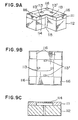
- Fig. 9 shows an embodiment of structure of a pressure sensor according to the present invention.
- Reference numeral 111 denotes a Si monocrystalline substrate and 112 denotes a borosilicate glass die.
- the central part of the Si monocrystalline substrate 111 is worked from its rear side to form a thin diaphragm 114.
- Borosilicate glass has a thermal expansion coefficient close to that of Si and is effective to realize stable operation of the sensor against the temperature change.
- the substrate lll and the glass die 112 are firmly bound by using the anodic bonding method, for example.
- a through hole 115 is provided at the central part of the glass die 112, a through hole 115 is provided. The pressure to be measured is applied via the through hole 115.
- MOS field effect transistors 113 and 113' are formed by using the IC technology. According to the applied pressure, the diaphragm 114 is deformed to apply stress upon MOS field effect transistors 113 and 113', forming a sensor, i.e. to the channel thereof.
- the FET 113 has a channel which is perpendicular to the edge of the diaphragm.
- the FET 113' has a channel which is in parallel to the edge of the diaphragm. Therefore the output voltage produced by the FET 113 for a pressure and that produced by the FET 113' for the same pressure change in opposing directions.
- Reference numeral 116 denotes a signal processing circuit including the above described operational amplifier and the voltage divider composed of resistors. By simultaneously forming the signal processing circuits 116 on the rigid portion of the Si substrate 111, a pressure sensor composed of a MOS IC may be realized.
- the present invention has been described by referring to embodiments of a pressure sensor.
- the present invention is not restricted to pressure sensors.
- the present invention may be applied to various sensors by forming a functional thin film on the gate electrode portion of the MOS structure. That is to say, a humidity sensor may be realized by using an organic polymer as the functional thin film.
- a gas sensor may be realized by using Pt, Pd or the like as the functional thin film.
- an ion (H + , Na + , K + or the like) sensor and a strain sensor may be realized respectively by using si 3 N 4 or the like and a piezoelectric film composed of ZnO or the like respectively as the functional thin film.
Abstract
Description
- The present invention relates to a semiconductor sensor and in particular to a semiconductor sensor having a voltage-controlled semiconductor active element.
- Various types of semiconductor sensors are known. A pressure or strain sensor comprising an insulated-gate (IG or MOS) active element and utilizing the piezoresistive effect is proposed in Solid State Electronics, vol. 18, 1975, p.p. 295 to 299. That paper discloses a bridge circuit comprising four metal-oxide-semiconductor field- effect-transistors (MOS FET's), a differential amplifier comprising two MOS FET's and so on. A strain gauge comprising a bridge circuit composed of four IG FET's is proposed in Japanese Patent Application Laid-Open No. 7699/80 which corresponds to U.S. Patent Application Serial No. 920,137 filed on June 28, 1978. Characteristics adjustment according to the species of diffusion impurities and the diffusion temperature is also implied. In addition, an IG FET utilizing the piezoresistive effect is disclosed in USP 3,609,252, for example. In all of the conventioanl sensors, however, pressure or the like is applied to a MOS FET with a constant gate voltage applied thereto. The resultant change in the drain current is detected to measure the quantity to be detected such as pressure. That is to say, a physical quantity is measured in an open loop state, resulting in low stability and reliability in measurement. Due to change in the drain current, the operation speed is restricted. In addition, the dissipated power is varied. Accordingly, the quantity of generated heat and the characteristics of the semiconductor sensor are also changed.
- Therefore, a semiconductor sensor which is more stable, highly reliable, highly sensitive and fast operable has been demanded.
- An object of the present invention is to provide a stable and highly sensitive semiconductor active element sensor having a negative feedback loop. To attain the object, the semiconductor active element may be formed by an insulated-gate field effect transistor (IG FET) having a channel structure responsive to a physical quantity to be measured. The drain voltage of the IG FET is negatively fed back to the gate thereof to let flow a nearly constant drain current through the IG FET. The stabilized drain current eliminates charging and discharging of the stray capacitance existing in the main current path, facilitating fast operation. Because of the stabilized drain current, the bias condition of the IG FET, and hence the power dissipation of the sensor are also stabilized. Therefore, the quantity of generated heat and hence the characteristics of the sensor are thermally stabilized.
- Another object of the present invention is to provide a semiconductor active element sensor comprising an insulated-gate field effect transistor (IG FET), a first amplifying means which is connected between the drain of the IG FET and the output terminal and has an amplification factor larger than unity, and a second amplifying means which is connected between the output terminal and the gate of the IG FET. The amplification factor of the first amplifying means is increased to provide a large output voltage. The amplification factor of the second amplifying means is adjusted to feed a stable bias to the gate of the IG FET. A capacitor for coupling the gate of the IG FET, to the source thereof may be placed in the second amplifying means so that a stable DC bias may be applied to the gate of the IG FET and the AC change in a physical quantity to be meansured may also be detected with high fidelity.
- Other objects, features and advantages of the present invention will be better understood and appreciated from the following description of embodiments taken in conjunction with drawings.
-
- Fig. 1 is a circuit diagram for illustrating an embodiment of the present invention;
- Fig. 2 shows the dependence of the characteristics of a MOS FET on the pressure;
- Fig. 3 shows the dependence of the characteristics of a MOS FET on the temperature;
- Fig. 4 is a circuit diagram for illustrating another embodiment of the present invention;
- Figs. 5 to 7 are circuit diagrams for illustrating examples of the embodiment shown in Fig. 4;
- Fig. 8 is a circuit diagram for illustrating still another embodiment of the present invention; and
- Figs. 9A to 9C are respectively a perspective view, a top view, and a sectional view for illustrating an embodiment of a pressure sensor according to the present invention.
- Embodiments of the present invention will now be described by referring to drawings.
-
- Fig. 1 shows an embodiment of the present invention.
- In Fig. 1, a fixed load impedance ZL and a voltage amplifying circuit A1 are connected to a drain D1 terminal 1 of a MOS FET Tl. The power supply voltage Vcc from the power source circuit PS is applied to the load impendance ZL. The gate G1 of the MOS FET T1 as well as the output terminal V are connected to the
output 2 of the amplifying circuit A1. The source terminal S1 of the MOS FET T1 is connected to the ground. The voltage gain of the amplifying circuit A1 is p. In addition, the MOS FET T1, i.e. the channel thereof, has a pressure sensitive amplifying function. - In this embodiment, the drain current variation ΔV1 caused by the pressure applied onto the MOS FET T1 is fed back to the gate terminal G1 of the MOS FET T1 via the amplifying circuit A1 having an amplification ratio µ, a feedback quantity ΔV0 (= µΔV1) being the change in the output voltage corresponding to the change in the applied pressure. The quantity of change ΔVg = ΔV0 in the gate bias serves to change the drain current Ids toward its original value. When the drain current Ids approaches its original value, the feedback quantity of the gate bias is decreased. The feedback quantity is stabilized at a point where the difference between the change in the drain current caused by the pressure and the change in the drain current caused by the negative feedback balances with the resultant gate bias.
- Fig. 2 shows an example of relationship between the drain current Ids of a MOS FET illustrated in Fig. 1 and the gate voltage Vgs thereof. It is assumed that a MOS FET has an enhancement mode n-channel and is subjected to a compressive stress in parallel with the channel direction. It corresponds to the tensile stress in parallel with a p-channel. Upon application of pressure, a characteristic curve A corresponding to zero applied stress is replaced by a curve B. If the pressure is applied with the constant gate voltage, a point P on the curve A corresponding to a current value Ido moves to a point R on the curve B, exhibiting the quantity of change |ΔIds(p)|. In the circuit of Fig. 1, the change in the drain current is transformed into the change in the drain voltage. The change in the drain voltage is amplified and negatively fed back to the gate G1 of the MOS FET T1. That is to say, the gate voltage is changed so as to cancel the change in the drain current. If the voltage gain p is infinitely high, the change in the drain current will be completely canceled.
- To restore the drain current to its original value Ido by changing the gate voltage, the operation point R must be moved to a point Q along the line B. At this time, the gate voltage changes from Vg(o) to V (p). The quantity of change expressed as ΔVg = Vg(p) - Vg(o) which corresponds to the strain caused by the applied pressure is fed to the output terminal as the quantity of change ΔVo in the output voltage.
- In Fig. 3, the drain current of a MOS FET as a function of the gate voltage thereof is plotted for various temperatures under an identical pressure. In the large current region, the carrier mobility is decreased to decrease the drain current Ids according as the temperature is raised. According as the temperature is raised in the small current region, the drain current Ids increases due to the reduced energy gap (red shift) and increase of thermally excited carriers. Midway between these two regions, there is a region around a point U in which the temperature variation exerts little influence on the drain current. By selecting a drain current value in the vicinity of the point U, a stable sensor which is not affected by the temperature may be realized. If the MOS FET with no stress being applied thereto is biased to a point where the minimum variation in characteristics due to the temperature is caused, the variation in characteristics such as the thermal drift due to the temperature may be substantially made zero at least in the strainless state.
- Fig. 4 shows another embodiment of the present invention. This embodiment has an advantage that desired magnitude of output voltage may be obtained irrespective of the negative feedback quantity to the gate.
- In this embodiment, a first amplifier A1 having an amplification ratio µ and a second amplifier N1 are connected between the drain terminal D1 of the MOS FET T1 and the gate terminal G1 thereof. The second or the negative feedback amplifier N1 has a voltage gain of β which is usually less than unity. In such configuration, the following equations ensure:


- By letting µ larger than unity and β smaller than unity, stable operation with a high output may be realized. In addition, the amplifier N1 may be constituted by using stable passive elements such as resistors and capacitors.
- Fig. 5 shows an example of the circuit illustrated in Fig. 4. In Fig. 5, the power supply voltage Vcc is fed to the drain terminal D1 of the MOS FET T1 through a resistor RL. The source terminal S1 of the MOS FET T1 is grounded. The noninverting input (+) of an operational amplifier A1 is connected to the drain terminal D1 of the MOS FET T1. A reference voltage source VB is connected to the inverting input (-) of the operational amplifier A1. The reference voltage source may be formed by a voltage divider circuit composed of diffusion resistors. An output terminal V for the detected value and a resistor R1 are connected to the
output terminal 2 of the operational amplifier A1. The gate terminal G1 of the MOS FET T1 is connected to theother terminal 3 of the resistor R1. - The operational amplifier A1 in this example corresponds to the first amplifier A1 illustrated in Fig. 4. The voltage divider circuit composed of resistors R1 and R2 corresponds to the second amplifier N1 illustrated in Fig. 4. The resistors R1 and R2 may be formed by using diffusion resistors or polysilicon resistors on the same semiconductor chip as that of the MOS FET.
- Owing to such configuration, the voltage V1 at the drain terminal D1 of the MOS FET T1 is always controlled to be equal to the reference voltage VB which is coupled to the inverting input terminal (-) of the above described operational amplifier A1. In addition, because of the voltage divider composed of resistors connected to the output terminal of the operational amplifier A1, the output voltage ΔV0 is obtained as a result of amplification with the ratio expressed as

- Fig. 6 shows another example of the circuit illustrated in Fig. 4. The circuit of Fig. 6 differs from that of Fig. 5 in that an
intermediate coupling point 3 of the voltage divider circuit, i.e., the gate terminal G1 of the MOS FET T1 is connected to the ground via a capacitor C1. - The capacitor C1 serves to eliminate the AC component in the gate bias and to feed back only the DC component to always keep constant the average drain current Id. Since the DC bias level is stabilized by the capacitor C1, the AC change in the quantity to be measured such as vibration may be detected with high precision.
- The capacitor C1 may be formed by providing a conductive region such as a doped polysilicon region on a thin insulative film which in turn is placed on a source region or a conductive member region having the same potential as that of the source.
- Fig. 7 shows still another example of the circuit illustrated in Fig. 4.
- The circuit of Fig. 7 differs from that of Fig. 5 in that the resistor RL in Fig. 5 is eliminated and a MOS field effect transistor T2 is inserted in the circuit. In an integrated circuit, the required occupation area may be greatly reduced by using a MOS field effect transistor instead of diffusion resistors, the chip size being reduced. Further, if the driver transistor T1 is configured to exhibit a piezoresistive effect which is different from that of the load transistor T2 for the same pressure, the sensitivity may be increased correspondingly. That is to say, if the MOS FET T1 and the MOS FET T2 are arranged on a Si diaphragm so that drain currents will change in directions opposing to each other upon pressure application (or so that the tensile stress and compressive stress will be incurred or so that the stress which is in parallel with the current channel and the stress which is perpendicular to the current channel will be incurred), the sensitivity may be increased correspondingly.
- The MOS FET T2 having a gate directly coupled to the drain and serving as a load may be replaced by another kind of transistor.
- In Fig. 8, instead of the transistor T2 illustrated in Fig. 7, a MOS field effect transistor having a conductivity type opposite to that of the driver transistor T1 is connected to the drive transistor T1 to form a pair of complementary transistors. The output voltage V is negatively fed back to gates of the above described two transistors to control the gate biases. As well known, such configuration provides a highly sensitive sensor which can be driven with extremely-low power dissipation. If the complementary configuration is applied to a pressure sensor as described in Fig. 7, it is possible to use -different piezoresistive effects of the n channel and p channel as they are without any contrivance. As a result, a highly sensitive sensor or a sensor with high precision may be easily realized.
- Fig. 9 shows an embodiment of structure of a pressure sensor according to the present invention. Reference numeral 111 denotes a Si monocrystalline substrate and 112 denotes a borosilicate glass die. The central part of the Si monocrystalline substrate 111 is worked from its rear side to form a
thin diaphragm 114. Borosilicate glass has a thermal expansion coefficient close to that of Si and is effective to realize stable operation of the sensor against the temperature change. In addition, the substrate lll and the glass die 112 are firmly bound by using the anodic bonding method, for example. At the central part of the glass die 112, a throughhole 115 is provided. The pressure to be measured is applied via the throughhole 115. On the upper surface of the above describedthin diaphragm 114, MOSfield effect transistors 113 and 113' are formed by using the IC technology. According to the applied pressure, thediaphragm 114 is deformed to apply stress upon MOSfield effect transistors 113 and 113', forming a sensor, i.e. to the channel thereof. TheFET 113 has a channel which is perpendicular to the edge of the diaphragm. The FET 113' has a channel which is in parallel to the edge of the diaphragm. Therefore the output voltage produced by theFET 113 for a pressure and that produced by the FET 113' for the same pressure change in opposing directions.Reference numeral 116 denotes a signal processing circuit including the above described operational amplifier and the voltage divider composed of resistors. By simultaneously forming thesignal processing circuits 116 on the rigid portion of the Si substrate 111, a pressure sensor composed of a MOS IC may be realized. - Heretofore, the present invention has been described by referring to embodiments of a pressure sensor. However, the present invention is not restricted to pressure sensors. The present invention may be applied to various sensors by forming a functional thin film on the gate electrode portion of the MOS structure. That is to say, a humidity sensor may be realized by using an organic polymer as the functional thin film. A gas sensor may be realized by using Pt, Pd or the like as the functional thin film. In the same way, an ion (H+, Na+, K+ or the like) sensor and a strain sensor may be realized respectively by using si3N4 or the like and a piezoelectric film composed of ZnO or the like respectively as the functional thin film.
Claims (14)
Applications Claiming Priority (2)
| Application Number | Priority Date | Filing Date | Title |
|---|---|---|---|
| JP57204668A JPS5995420A (en) | 1982-11-24 | 1982-11-24 | Mos type sensor |
| JP204668/82 | 1982-11-24 |
Publications (3)
| Publication Number | Publication Date |
|---|---|
| EP0118605A2 true EP0118605A2 (en) | 1984-09-19 |
| EP0118605A3 EP0118605A3 (en) | 1985-05-29 |
| EP0118605B1 EP0118605B1 (en) | 1988-02-24 |
Family
ID=16494305
Family Applications (1)
| Application Number | Title | Priority Date | Filing Date |
|---|---|---|---|
| EP83111718A Expired EP0118605B1 (en) | 1982-11-24 | 1983-11-23 | Feedback circuit for a semiconductor active element sensor |
Country Status (4)
| Country | Link |
|---|---|
| US (1) | US4633099A (en) |
| EP (1) | EP0118605B1 (en) |
| JP (1) | JPS5995420A (en) |
| DE (1) | DE3375739D1 (en) |
Cited By (3)
| Publication number | Priority date | Publication date | Assignee | Title |
|---|---|---|---|---|
| EP0441324A1 (en) * | 1990-02-06 | 1991-08-14 | Honda Giken Kogyo Kabushiki Kaisha | Semiconductor sensor |
| WO2006002535A1 (en) * | 2004-06-30 | 2006-01-12 | Universite De Sherbrooke | Sensor arrays based on electronic oscillators |
| WO2012101257A1 (en) | 2011-01-28 | 2012-08-02 | Elmos Semiconductor Ag | Microelectromechanical component and method for testing a microelectromechanical component |
Families Citing this family (14)
| Publication number | Priority date | Publication date | Assignee | Title |
|---|---|---|---|---|
| US4818895A (en) * | 1987-11-13 | 1989-04-04 | Kaufman Lance R | Direct current sense lead |
| DE68926601T2 (en) * | 1988-09-02 | 1997-01-23 | Honda Motor Co Ltd | Semiconductor sensor |
| JPH03123439U (en) * | 1990-03-23 | 1991-12-16 | ||
| JPH04105369A (en) * | 1990-08-24 | 1992-04-07 | Honda Motor Co Ltd | Semiconductor sensor |
| US5397911A (en) * | 1991-04-02 | 1995-03-14 | Honda Giken Kogyo Kabushiki Kaisha | Semiconductor sensor with plural gate electrodes |
| JP3009239B2 (en) * | 1991-04-02 | 2000-02-14 | 本田技研工業株式会社 | Semiconductor sensor |
| JP3281217B2 (en) * | 1995-05-23 | 2002-05-13 | 富士電機株式会社 | Semiconductor type acceleration sensor and method for evaluating characteristics of sensor element of the sensor |
| JP2852886B2 (en) * | 1995-09-04 | 1999-02-03 | 本田技研工業株式会社 | Semiconductor stress sensor |
| US6621131B2 (en) * | 2001-11-01 | 2003-09-16 | Intel Corporation | Semiconductor transistor having a stressed channel |
| DE102004016155B3 (en) * | 2004-04-01 | 2006-05-24 | Infineon Technologies Ag | Force sensor with organic field effect transistors, pressure sensor based thereon, position sensor and fingerprint sensor |
| JP2015075623A (en) * | 2013-10-09 | 2015-04-20 | セイコーエプソン株式会社 | Light-emitting device, electronic apparatus, and light-emitting device design method |
| JP6287025B2 (en) * | 2013-10-09 | 2018-03-07 | セイコーエプソン株式会社 | LIGHT EMITTING DEVICE AND ELECTRONIC DEVICE |
| CN105758898B (en) * | 2016-04-15 | 2019-02-26 | 中国科学院过程工程研究所 | A kind of highly sensitive self feed back type gas sensor warning circuit |
| JP2022550234A (en) * | 2019-06-24 | 2022-12-01 | アルベルト-ルドビクス-ウニベルジテート フライブルク | Tactile sensor and method of operating the tactile sensor |
Citations (2)
| Publication number | Priority date | Publication date | Assignee | Title |
|---|---|---|---|---|
| US4176555A (en) * | 1978-08-07 | 1979-12-04 | Mechanical Technology Incorporated | Signal amplifier system for controlled carrier signal measuring sensor/transducer of the variable impedance type |
| US4390879A (en) * | 1980-02-15 | 1983-06-28 | Hokushin Electric Works, Ltd. | Apparatus for converting physical quantities |
Family Cites Families (15)
| Publication number | Priority date | Publication date | Assignee | Title |
|---|---|---|---|---|
| US3609252A (en) * | 1967-01-23 | 1971-09-28 | Texas Instruments Inc | Transducer apparatus and system utilizing insulated gate semiconductor field effect devices |
| US3749984A (en) * | 1969-04-11 | 1973-07-31 | Rca Corp | Electroacoustic semiconductor device employing an igfet |
| US3582690A (en) * | 1969-06-09 | 1971-06-01 | Gen Electric | Semiconductor strain sensor with controlled sensitivity |
| US3805096A (en) * | 1973-01-22 | 1974-04-16 | W Hamilton | Coded touch multifunction touch control switch circuitry |
| GB1443174A (en) * | 1973-04-06 | 1976-07-21 | Alphameric Keyboards Ltd | Keyboards for electronic circuits |
| US4081700A (en) * | 1976-06-16 | 1978-03-28 | Hamilton Ii William F | Touch control switch circuit with compensation for power supply line fluctuations |
| US4173900A (en) * | 1977-03-07 | 1979-11-13 | Hitachi, Ltd. | Semiconductor pressure transducer |
| JPS547699A (en) * | 1977-06-20 | 1979-01-20 | Hitachi Ltd | Method of dressing wire-out electric-discharge processing electrodes |
| US4263659A (en) * | 1978-03-27 | 1981-04-21 | Canon Kabushiki Kaisha | Electronic instrument with a flexible keyboard |
| CH623195B (en) * | 1978-04-11 | 1900-01-01 | Ebauches Sa | ELECTRONIC WATCH WITH MEANS OF CONTROL AND SELECTION OF FUNCTIONS. |
| DE2841312C2 (en) * | 1978-09-22 | 1985-06-05 | Robert Bosch Gmbh, 7000 Stuttgart | Monolithic semiconductor pressure sensor and process for its manufacture |
| JPS55112864U (en) * | 1979-02-02 | 1980-08-08 | ||
| US4205556A (en) * | 1979-02-12 | 1980-06-03 | Rockwell International Corporation | Circuitry for strain sensitive apparatus |
| US4378578A (en) * | 1980-01-14 | 1983-03-29 | Pioneer Ansafone Manufacturing Corporation | Mode control device for tape recorders |
| JPS5952727A (en) * | 1982-09-20 | 1984-03-27 | Hitachi Ltd | Semiconductor pressure sensor |
-
1982
- 1982-11-24 JP JP57204668A patent/JPS5995420A/en active Granted
-
1983
- 1983-11-22 US US06/554,332 patent/US4633099A/en not_active Expired - Fee Related
- 1983-11-23 DE DE8383111718T patent/DE3375739D1/en not_active Expired
- 1983-11-23 EP EP83111718A patent/EP0118605B1/en not_active Expired
Patent Citations (2)
| Publication number | Priority date | Publication date | Assignee | Title |
|---|---|---|---|---|
| US4176555A (en) * | 1978-08-07 | 1979-12-04 | Mechanical Technology Incorporated | Signal amplifier system for controlled carrier signal measuring sensor/transducer of the variable impedance type |
| US4390879A (en) * | 1980-02-15 | 1983-06-28 | Hokushin Electric Works, Ltd. | Apparatus for converting physical quantities |
Non-Patent Citations (1)
| Title |
|---|
| Elektronic, Vol. 18, No. 12, December 1969, pages 377-379. Munchen (DE) "Pitran, ein Druckempfindlicher Transistor". * |
Cited By (5)
| Publication number | Priority date | Publication date | Assignee | Title |
|---|---|---|---|---|
| EP0441324A1 (en) * | 1990-02-06 | 1991-08-14 | Honda Giken Kogyo Kabushiki Kaisha | Semiconductor sensor |
| WO2006002535A1 (en) * | 2004-06-30 | 2006-01-12 | Universite De Sherbrooke | Sensor arrays based on electronic oscillators |
| US7428851B2 (en) | 2004-06-30 | 2008-09-30 | Universite De Sherbrooke | Sensor arrays based on electronic oscillators |
| WO2012101257A1 (en) | 2011-01-28 | 2012-08-02 | Elmos Semiconductor Ag | Microelectromechanical component and method for testing a microelectromechanical component |
| US9399572B2 (en) | 2011-01-28 | 2016-07-26 | Elmos Semiconductor Ag | Microelectromechanical component and method for testing a microelectromechanical component |
Also Published As
| Publication number | Publication date |
|---|---|
| EP0118605B1 (en) | 1988-02-24 |
| JPS5995420A (en) | 1984-06-01 |
| US4633099A (en) | 1986-12-30 |
| EP0118605A3 (en) | 1985-05-29 |
| DE3375739D1 (en) | 1988-03-31 |
| JPH0159525B2 (en) | 1989-12-18 |
Similar Documents
| Publication | Publication Date | Title |
|---|---|---|
| EP0118605B1 (en) | Feedback circuit for a semiconductor active element sensor | |
| EP0409213B1 (en) | Amplifiying compensation circuit for semiconductor pressure sensor | |
| US4657658A (en) | Semiconductor devices | |
| US4910455A (en) | Non-intrusive current measuring circuit | |
| US4716307A (en) | Regulated power supply for semiconductor chips with compensation for changes in electrical characteristics or chips and in external power supply | |
| US6615668B2 (en) | Semiconductor pressure sensor having signal processor circuit | |
| EP0358352B1 (en) | Temperature compensation circuit | |
| US3582690A (en) | Semiconductor strain sensor with controlled sensitivity | |
| EP0237280A2 (en) | Magnetic sensor | |
| US10197464B2 (en) | Semiconductor physical quantity sensor having filter circuits for blocking electromagnetic wave noise | |
| EP0773437A2 (en) | Temperature sensing device and applications thereof | |
| JP3009239B2 (en) | Semiconductor sensor | |
| US4766655A (en) | Method for fabricating a compensated silicon pressure sensing device | |
| JPH052037A (en) | Zero cross detecting circuit | |
| US4672853A (en) | Apparatus and method for a pressure-sensitive device | |
| US5319319A (en) | Low drift resistor structure for amplifiers | |
| JP3520652B2 (en) | Semiconductor force sensor | |
| JP2641104B2 (en) | Semiconductor stress sensor | |
| EP1682858B1 (en) | An integrated thermal sensor for microwave transistors | |
| US4611129A (en) | Signal conversion circuit | |
| Clark | Split-drain MOSFET magnetic sensor arrays | |
| EP0664609B1 (en) | Buffer for sensor | |
| JP3075635B2 (en) | Temperature compensated amplifier | |
| JP3237256B2 (en) | Acceleration detection circuit | |
| JP2553826B2 (en) | Semiconductor sensor |
Legal Events
| Date | Code | Title | Description |
|---|---|---|---|
| PUAI | Public reference made under article 153(3) epc to a published international application that has entered the european phase |
Free format text: ORIGINAL CODE: 0009012 |
|
| AK | Designated contracting states |
Designated state(s): DE FR GB |
|
| PUAL | Search report despatched |
Free format text: ORIGINAL CODE: 0009013 |
|
| AK | Designated contracting states |
Designated state(s): DE FR GB |
|
| 17P | Request for examination filed |
Effective date: 19850530 |
|
| 17Q | First examination report despatched |
Effective date: 19860918 |
|
| GRAA | (expected) grant |
Free format text: ORIGINAL CODE: 0009210 |
|
| AK | Designated contracting states |
Kind code of ref document: B1 Designated state(s): DE FR GB |
|
| REF | Corresponds to: |
Ref document number: 3375739 Country of ref document: DE Date of ref document: 19880331 |
|
| ET | Fr: translation filed | ||
| PLBE | No opposition filed within time limit |
Free format text: ORIGINAL CODE: 0009261 |
|
| STAA | Information on the status of an ep patent application or granted ep patent |
Free format text: STATUS: NO OPPOSITION FILED WITHIN TIME LIMIT |
|
| 26N | No opposition filed | ||
| PGFP | Annual fee paid to national office [announced via postgrant information from national office to epo] |
Ref country code: FR Payment date: 19910930 Year of fee payment: 9 |
|
| PGFP | Annual fee paid to national office [announced via postgrant information from national office to epo] |
Ref country code: GB Payment date: 19911113 Year of fee payment: 9 |
|
| PGFP | Annual fee paid to national office [announced via postgrant information from national office to epo] |
Ref country code: DE Payment date: 19920120 Year of fee payment: 9 |
|
| PG25 | Lapsed in a contracting state [announced via postgrant information from national office to epo] |
Ref country code: GB Effective date: 19921123 |
|
| GBPC | Gb: european patent ceased through non-payment of renewal fee |
Effective date: 19921123 |
|
| PG25 | Lapsed in a contracting state [announced via postgrant information from national office to epo] |
Ref country code: FR Effective date: 19930730 |
|
| PG25 | Lapsed in a contracting state [announced via postgrant information from national office to epo] |
Ref country code: DE Effective date: 19930803 |
|
| REG | Reference to a national code |
Ref country code: FR Ref legal event code: ST |