EP0115591B1 - Photodiode and photodetector comprising an integrated series of photodiodes - Google Patents
Photodiode and photodetector comprising an integrated series of photodiodes Download PDFInfo
- Publication number
- EP0115591B1 EP0115591B1 EP83112245A EP83112245A EP0115591B1 EP 0115591 B1 EP0115591 B1 EP 0115591B1 EP 83112245 A EP83112245 A EP 83112245A EP 83112245 A EP83112245 A EP 83112245A EP 0115591 B1 EP0115591 B1 EP 0115591B1
- Authority
- EP
- European Patent Office
- Prior art keywords
- region
- photodiode
- undoped
- regions
- light
- Prior art date
- Legal status (The legal status is an assumption and is not a legal conclusion. Google has not performed a legal analysis and makes no representation as to the accuracy of the status listed.)
- Expired
Links
- 239000004065 semiconductor Substances 0.000 claims description 25
- 229910001218 Gallium arsenide Inorganic materials 0.000 claims description 11
- 239000002800 charge carrier Substances 0.000 claims description 4
- 239000000969 carrier Substances 0.000 description 18
- 239000000463 material Substances 0.000 description 11
- JBRZTFJDHDCESZ-UHFFFAOYSA-N AsGa Chemical compound [As]#[Ga] JBRZTFJDHDCESZ-UHFFFAOYSA-N 0.000 description 10
- 238000000034 method Methods 0.000 description 6
- 230000004044 response Effects 0.000 description 4
- 238000006243 chemical reaction Methods 0.000 description 3
- 238000010586 diagram Methods 0.000 description 3
- 238000009792 diffusion process Methods 0.000 description 3
- 239000000835 fiber Substances 0.000 description 3
- 230000007704 transition Effects 0.000 description 3
- 238000004891 communication Methods 0.000 description 2
- 230000002596 correlated effect Effects 0.000 description 2
- 230000005684 electric field Effects 0.000 description 2
- 238000001451 molecular beam epitaxy Methods 0.000 description 2
- 230000003287 optical effect Effects 0.000 description 2
- 230000035515 penetration Effects 0.000 description 2
- 239000000758 substrate Substances 0.000 description 2
- 230000001052 transient effect Effects 0.000 description 2
- 238000010521 absorption reaction Methods 0.000 description 1
- 230000001133 acceleration Effects 0.000 description 1
- 230000004888 barrier function Effects 0.000 description 1
- 239000013078 crystal Substances 0.000 description 1
- 230000001419 dependent effect Effects 0.000 description 1
- 239000002019 doping agent Substances 0.000 description 1
- 230000000694 effects Effects 0.000 description 1
- 230000005670 electromagnetic radiation Effects 0.000 description 1
- 238000005286 illumination Methods 0.000 description 1
- 230000006872 improvement Effects 0.000 description 1
- 239000012535 impurity Substances 0.000 description 1
- 230000031700 light absorption Effects 0.000 description 1
- 231100000614 poison Toxicity 0.000 description 1
- 230000007096 poisonous effect Effects 0.000 description 1
- 230000000750 progressive effect Effects 0.000 description 1
- 238000007493 shaping process Methods 0.000 description 1
- 238000001228 spectrum Methods 0.000 description 1
- 230000001629 suppression Effects 0.000 description 1
- 230000007723 transport mechanism Effects 0.000 description 1
Images
Classifications
-
- H—ELECTRICITY
- H10—SEMICONDUCTOR DEVICES; ELECTRIC SOLID-STATE DEVICES NOT OTHERWISE PROVIDED FOR
- H10F—INORGANIC SEMICONDUCTOR DEVICES SENSITIVE TO INFRARED RADIATION, LIGHT, ELECTROMAGNETIC RADIATION OF SHORTER WAVELENGTH OR CORPUSCULAR RADIATION
- H10F39/00—Integrated devices, or assemblies of multiple devices, comprising at least one element covered by group H10F30/00, e.g. radiation detectors comprising photodiode arrays
- H10F39/10—Integrated devices
- H10F39/107—Integrated devices having multiple elements covered by H10F30/00 in a repetitive configuration, e.g. radiation detectors comprising photodiode arrays
-
- H—ELECTRICITY
- H10—SEMICONDUCTOR DEVICES; ELECTRIC SOLID-STATE DEVICES NOT OTHERWISE PROVIDED FOR
- H10F—INORGANIC SEMICONDUCTOR DEVICES SENSITIVE TO INFRARED RADIATION, LIGHT, ELECTROMAGNETIC RADIATION OF SHORTER WAVELENGTH OR CORPUSCULAR RADIATION
- H10F30/00—Individual radiation-sensitive semiconductor devices in which radiation controls the flow of current through the devices, e.g. photodetectors
- H10F30/20—Individual radiation-sensitive semiconductor devices in which radiation controls the flow of current through the devices, e.g. photodetectors the devices having potential barriers, e.g. phototransistors
- H10F30/21—Individual radiation-sensitive semiconductor devices in which radiation controls the flow of current through the devices, e.g. photodetectors the devices having potential barriers, e.g. phototransistors the devices being sensitive to infrared, visible or ultraviolet radiation
- H10F30/22—Individual radiation-sensitive semiconductor devices in which radiation controls the flow of current through the devices, e.g. photodetectors the devices having potential barriers, e.g. phototransistors the devices being sensitive to infrared, visible or ultraviolet radiation the devices having only one potential barrier, e.g. photodiodes
- H10F30/222—Individual radiation-sensitive semiconductor devices in which radiation controls the flow of current through the devices, e.g. photodetectors the devices having potential barriers, e.g. phototransistors the devices being sensitive to infrared, visible or ultraviolet radiation the devices having only one potential barrier, e.g. photodiodes the potential barrier being a PN heterojunction
-
- H—ELECTRICITY
- H10—SEMICONDUCTOR DEVICES; ELECTRIC SOLID-STATE DEVICES NOT OTHERWISE PROVIDED FOR
- H10F—INORGANIC SEMICONDUCTOR DEVICES SENSITIVE TO INFRARED RADIATION, LIGHT, ELECTROMAGNETIC RADIATION OF SHORTER WAVELENGTH OR CORPUSCULAR RADIATION
- H10F77/00—Constructional details of devices covered by this subclass
- H10F77/10—Semiconductor bodies
- H10F77/14—Shape of semiconductor bodies; Shapes, relative sizes or dispositions of semiconductor regions within semiconductor bodies
Definitions
- This invention relates to photodiodes and photodetectors comprising an integrated series of photodiodes.
- Semiconductor devices which convert optical energy to electrical energy operate on the principle that the light produces carriers in the semiconductor that in turn travel a distance within the device structure to a location where those carriers operate to deliver an output current.
- Light wavelengths penetrate the semiconductor to different depths and produce different quantities of carriers. The number of carriers produced and the distance they must travel are considerations in the design of the structure.
- US-A-4 127 862 discloses an integrated multilayer photodetector wherein doped layers of different thicknesses are joined with a low impedance contact, by using quantum mechanical tunnelling junctions for the purpose of absorbing more of the monochromatic light and to produce a high voltage output.
- the device of US ⁇ A ⁇ 4 127 862 however employs separate multiheterolayer photodiodes connected by separate tunnelling junctions of the order of 100 nm (1000 Angstroms) in thickness, the resulting photocurrent occurs primarily by diffusion, and reports an output voltage of the order of 1.75 V using the semiconductor materials GaAs and AIGaAs.
- the invention involves a semiconductor optical-to-electrical conversion principle in which an absorbing element of an undoped region bounded by a thin tunnelling junction together act as a unit to provide a high performance.
- the carriers are produced in an undoped region which provides a high field for carrier acceleration and relatively collision free movement over a significant portion of the undoped region.
- the undoped region is bounded by a thin, of the order of the mean free path of an electron, quantum mechanical tunnelling junction.
- the thickness of the undoped region is of the order of the ballistic transport thickness for a carrier in the material selected.
- a photodiode consists, according to the invention, of an undoped light-absorbing semiconductor region contiguous with one component region of a pair of doped semiconductor regions forming a quantum mechanical tunnelling pn junction, the combined thickness of the pair of doped semiconductor regions being of the order of the mean free path length of a charge carrier therein, and the undoped light-absorbing semiconductor region having a thickness of the order of the ballistic transport distance of a charge carrier in that region.
- the two criteria operate to provide a condition where a carrier is moved primarily by drift rather than diffusion resulting in more carriers being effective, providing thereby increased efficiency and since the carriers can move more rapidly, faster turn-on and turn-off occurs in the 10- 12 second range.
- the undoped region should be sufficiently intrinsic that a high field is produced in the presence of light generated carriers. This is generally less than 10 16 atoms per cm 3 in most materials.
- the dimensions of the undoped region should be at least sufficient for substantial carrier generation but not exceeding the distance over which a substantial portion of the carriers would travel ballistically. This of the range of about 50 to 300 nm (500 to 3000A) for most materials.
- the boundary p and n regions that form the tunnelling p-n junctions should be of the order of the mean free path length of an electron in the semiconductor being used from the undoped region through the heavily doped region. This is around 5 nm (50A) in most materials.
- the invention is particularly useful with monochromatic light.
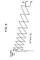
- a plurality of undoped regions may be employed, each near ballistic transport thickness and becoming progressively thicker away from the surface and each joined to the adjacent one at the mean free path of an electron thickness quantum mechanical tunnelling junction with the total of all regions not exceeding the penetration depth of the light.
- the progressively thicker undoped regions are designed to have equal quantities of carriers in each region.
- the progressive thickness increase away from the surface is due to the exponential decay dependence of the absorption of light.
- each undoped region has an impurity concentration less than 10 16 atoms per cm 3 and the boundary p-n junctions of the progressively thicker regions are measured from the light incident surface.
- the regions vary from about 50 to 350 nm (500 to 3500A).
- the boundary thickness of the p + and n + regions for the tunnelling junctions is of the order of the mean free path of an electron which for GaAs is about 5 nm (50A).
- the substrate is provided with high n + conductivity to facilitate external circuit connection.
- the second external circuit connection would be made to the light incident surface using the standard light receiving surface techniques of translucent electrodes or grids.
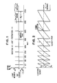
- E c , E F and E v are the conduction band energy level, the Fermi level and the valence band energy levels, respectively.
- the thicknesses of the GaAs sections are designed so that the same number of hole electron pairs are produced in each of the sections when the device is illuminated by a monochromatic light source of a particular wavelength.
- the sections become thicker away from the surface with the thickest being labelled Wg.
- the total thickness and thus the number of sections is governed by the effective penetration depth of the light in the particular semiconductor material.
- C will be equal to 0.1
- ⁇ ( ⁇ ) will be equal to 2x10 4 cm -1
- the energy gap width is 1.42 eV.
- the transient response of the device of this invention is limited by the transit time of the photogenerated carriers in the section, W s . This is because the photocurrent is collected simultaneously by all of the sections with the thickest section Wg being the slowest.
- the transit time is as expressed in Equation 3.
- the 0.35 picosecond transit time of the structure of Figure 1 is substantially a thirty- fold improvement in transit time.
- the response time of a device would also include the time required for ballistic carriers to thermalize to the bond edge.
- Structures employing the principles of the invention are directly compatible with semiconductor circuitry and are useful for the direct rectification and mixing of electromagnetic radiation at light wavelengths.
- Figure 1 may be fabricated by the technique well known in the art of molecular beam epitaxy wherein through the use of a molecular beam both the material of the crystal and the resultant dopant are provided together in an epitaxial layer with each layer and each boundary being precisely grown from the substrate.
- the p * GaAs regions in the device be realised using Mg doping rather than Be doping as is used in most prior art devices.
- the Be is poisonous and requires great care.
- Efficient doping with Mg is achieved using a special volatile oxide suppression technique.
- the principles of the invention are applicable to many semiconductor materials, including Si and GaAs, the ones receiving the most attention at this state of the art.
Landscapes
- Light Receiving Elements (AREA)
Applications Claiming Priority (2)
| Application Number | Priority Date | Filing Date | Title |
|---|---|---|---|
| US06/454,784 US4525731A (en) | 1982-12-30 | 1982-12-30 | Semiconductor conversion of optical-to-electrical energy |
| US454784 | 1982-12-30 |
Publications (3)
| Publication Number | Publication Date |
|---|---|
| EP0115591A2 EP0115591A2 (en) | 1984-08-15 |
| EP0115591A3 EP0115591A3 (en) | 1986-03-12 |
| EP0115591B1 true EP0115591B1 (en) | 1988-05-18 |
Family
ID=23806069
Family Applications (1)
| Application Number | Title | Priority Date | Filing Date |
|---|---|---|---|
| EP83112245A Expired EP0115591B1 (en) | 1982-12-30 | 1983-12-06 | Photodiode and photodetector comprising an integrated series of photodiodes |
Country Status (4)
| Country | Link |
|---|---|
| US (1) | US4525731A (enExample) |
| EP (1) | EP0115591B1 (enExample) |
| JP (1) | JPS59124776A (enExample) |
| DE (1) | DE3376712D1 (enExample) |
Families Citing this family (11)
| Publication number | Priority date | Publication date | Assignee | Title |
|---|---|---|---|---|
| US4590507A (en) * | 1984-07-31 | 1986-05-20 | At&T Bell Laboratories | Variable gap devices |
| US4745452A (en) * | 1984-09-24 | 1988-05-17 | Massachusetts Institute Of Technology | Tunneling transfer devices |
| US4882609A (en) * | 1984-11-19 | 1989-11-21 | Max-Planck Gesellschaft Zur Forderung Der Wissenschafter E.V. | Semiconductor devices with at least one monoatomic layer of doping atoms |
| US5060234A (en) * | 1984-11-19 | 1991-10-22 | Max-Planck Gesellschaft Zur Forderung Der Wissenschaften | Injection laser with at least one pair of monoatomic layers of doping atoms |
| US5216260A (en) * | 1984-11-19 | 1993-06-01 | Max-Planck Gesellschaft Zur Foerderung Der Wissenschaften E.V. | Optically bistable semiconductor device with pairs of monoatomic layers separated by intrinsic layers |
| JPS62183570A (ja) * | 1986-02-07 | 1987-08-11 | Mitsubishi Electric Corp | 光検出装置 |
| US4894526A (en) * | 1987-01-15 | 1990-01-16 | American Telephone And Telegraph Company, At&T Bell Laboratories | Infrared-radiation detector device |
| US4903101A (en) * | 1988-03-28 | 1990-02-20 | California Institute Of Technology | Tunable quantum well infrared detector |
| US5047810A (en) * | 1989-01-09 | 1991-09-10 | At&T Bell Laboratories | Optically controlled resonant tunneling electronic devices |
| US6417528B1 (en) * | 2000-01-28 | 2002-07-09 | Agere Systems Guardian Corp. | High speed semiconductor photodetector |
| US7619159B1 (en) * | 2002-05-17 | 2009-11-17 | Ugur Ortabasi | Integrating sphere photovoltaic receiver (powersphere) for laser light to electric power conversion |
Family Cites Families (4)
| Publication number | Priority date | Publication date | Assignee | Title |
|---|---|---|---|---|
| US4127862A (en) * | 1977-09-06 | 1978-11-28 | Bell Telephone Laboratories, Incorporated | Integrated optical detectors |
| US4179702A (en) * | 1978-03-09 | 1979-12-18 | Research Triangle Institute | Cascade solar cells |
| US4332974A (en) * | 1979-06-28 | 1982-06-01 | Chevron Research Company | Multilayer photovoltaic cell |
| US4282541A (en) * | 1979-12-26 | 1981-08-04 | Bell Telephone Laboratories, Incorporated | Planar P-I-N photodetectors |
-
1982
- 1982-12-30 US US06/454,784 patent/US4525731A/en not_active Expired - Lifetime
-
1983
- 1983-09-20 JP JP58172342A patent/JPS59124776A/ja active Granted
- 1983-12-06 DE DE8383112245T patent/DE3376712D1/de not_active Expired
- 1983-12-06 EP EP83112245A patent/EP0115591B1/en not_active Expired
Also Published As
| Publication number | Publication date |
|---|---|
| EP0115591A2 (en) | 1984-08-15 |
| DE3376712D1 (en) | 1988-06-23 |
| JPS59124776A (ja) | 1984-07-18 |
| US4525731A (en) | 1985-06-25 |
| JPS6260824B2 (enExample) | 1987-12-18 |
| EP0115591A3 (en) | 1986-03-12 |
Similar Documents
| Publication | Publication Date | Title |
|---|---|---|
| EP0084621B1 (en) | Semiconductor signal conversion device using photon coupling | |
| US6288415B1 (en) | Optoelectronic semiconductor devices | |
| US4202000A (en) | Diode capable of alternately functioning as an emitter and detector of light of the same wavelength | |
| US6888179B2 (en) | GaAs substrate with Sb buffering for high in devices | |
| Decoster et al. | Optoelectronic sensors | |
| JP2934294B2 (ja) | アバランシェフォトダイオード | |
| EP0115591B1 (en) | Photodiode and photodetector comprising an integrated series of photodiodes | |
| WO1989012323A1 (en) | Novel high-speed integrated heterostructure transistors, photodetectors, and optoelectronic circuits | |
| Bornholdt et al. | Waveguide-integrated pin photodiode on InP | |
| CA2050435C (en) | Photo-sensing device | |
| US4390889A (en) | Photodiode having an InGaAs layer with an adjacent InGaAsP p-n junction | |
| EP0113074B1 (en) | Method of logically combining optical signals | |
| EP0063421B1 (en) | High speed photoconductive detector | |
| EP0304048B1 (en) | A planar type heterostructure avalanche photodiode | |
| EP1470574B9 (en) | High speed pin photodiode with increased responsivity | |
| US4282541A (en) | Planar P-I-N photodetectors | |
| US4816890A (en) | Optoelectronic device | |
| US4021833A (en) | Infrared photodiode | |
| US4112457A (en) | Photovoltaic device having an extended PN junction | |
| US5281844A (en) | Avalanche photodiode | |
| Kim et al. | Barrier height enhancement of InP-based n-Ga0. 47In0. 53As Schottky-barrier diodes grown by molecular beam epitaxy | |
| GB2094551A (en) | Photon feedback photodetectors | |
| RU2080690C1 (ru) | Фотовольтаический преобразователь | |
| Li | Photonic devices | |
| RU2676188C1 (ru) | Свч фотоприемник лазерного излучения |
Legal Events
| Date | Code | Title | Description |
|---|---|---|---|
| PUAI | Public reference made under article 153(3) epc to a published international application that has entered the european phase |
Free format text: ORIGINAL CODE: 0009012 |
|
| AK | Designated contracting states |
Designated state(s): DE FR GB |
|
| 17P | Request for examination filed |
Effective date: 19841029 |
|
| PUAL | Search report despatched |
Free format text: ORIGINAL CODE: 0009013 |
|
| AK | Designated contracting states |
Kind code of ref document: A3 Designated state(s): DE FR GB |
|
| 17Q | First examination report despatched |
Effective date: 19870730 |
|
| R17C | First examination report despatched (corrected) |
Effective date: 19870804 |
|
| GRAA | (expected) grant |
Free format text: ORIGINAL CODE: 0009210 |
|
| AK | Designated contracting states |
Kind code of ref document: B1 Designated state(s): DE FR GB |
|
| REF | Corresponds to: |
Ref document number: 3376712 Country of ref document: DE Date of ref document: 19880623 |
|
| ET | Fr: translation filed | ||
| PLBE | No opposition filed within time limit |
Free format text: ORIGINAL CODE: 0009261 |
|
| STAA | Information on the status of an ep patent application or granted ep patent |
Free format text: STATUS: NO OPPOSITION FILED WITHIN TIME LIMIT |
|
| 26N | No opposition filed | ||
| PGFP | Annual fee paid to national office [announced via postgrant information from national office to epo] |
Ref country code: GB Payment date: 19931124 Year of fee payment: 11 |
|
| PGFP | Annual fee paid to national office [announced via postgrant information from national office to epo] |
Ref country code: FR Payment date: 19931129 Year of fee payment: 11 |
|
| PGFP | Annual fee paid to national office [announced via postgrant information from national office to epo] |
Ref country code: DE Payment date: 19931221 Year of fee payment: 11 |
|
| PG25 | Lapsed in a contracting state [announced via postgrant information from national office to epo] |
Ref country code: GB Effective date: 19941206 |
|
| GBPC | Gb: european patent ceased through non-payment of renewal fee |
Effective date: 19941206 |
|
| PG25 | Lapsed in a contracting state [announced via postgrant information from national office to epo] |
Ref country code: FR Effective date: 19950831 |
|
| PG25 | Lapsed in a contracting state [announced via postgrant information from national office to epo] |
Ref country code: DE Effective date: 19950901 |
|
| REG | Reference to a national code |
Ref country code: FR Ref legal event code: ST |