EP0115445A2 - Optical heterodyne detection pulse receiving system and method - Google Patents
Optical heterodyne detection pulse receiving system and method Download PDFInfo
- Publication number
- EP0115445A2 EP0115445A2 EP84300603A EP84300603A EP0115445A2 EP 0115445 A2 EP0115445 A2 EP 0115445A2 EP 84300603 A EP84300603 A EP 84300603A EP 84300603 A EP84300603 A EP 84300603A EP 0115445 A2 EP0115445 A2 EP 0115445A2
- Authority
- EP
- European Patent Office
- Prior art keywords
- signal
- pulse
- intermediate frequency
- frequency
- modulated
- Prior art date
- Legal status (The legal status is an assumption and is not a legal conclusion. Google has not performed a legal analysis and makes no representation as to the accuracy of the status listed.)
- Ceased
Links
- 230000003287 optical effect Effects 0.000 title claims description 41
- 238000001514 detection method Methods 0.000 title claims description 14
- 238000000034 method Methods 0.000 title claims description 12
- 230000001360 synchronised effect Effects 0.000 claims description 11
- 238000006243 chemical reaction Methods 0.000 claims 1
- 230000001172 regenerating effect Effects 0.000 claims 1
- 239000004065 semiconductor Substances 0.000 description 10
- 230000035945 sensitivity Effects 0.000 description 5
- 238000010586 diagram Methods 0.000 description 4
- 230000008929 regeneration Effects 0.000 description 4
- 238000011069 regeneration method Methods 0.000 description 4
- 230000003321 amplification Effects 0.000 description 2
- 230000006866 deterioration Effects 0.000 description 2
- 238000005516 engineering process Methods 0.000 description 2
- 239000000284 extract Substances 0.000 description 2
- 238000000605 extraction Methods 0.000 description 2
- 229910052732 germanium Inorganic materials 0.000 description 2
- GNPVGFCGXDBREM-UHFFFAOYSA-N germanium atom Chemical compound [Ge] GNPVGFCGXDBREM-UHFFFAOYSA-N 0.000 description 2
- 238000003199 nucleic acid amplification method Methods 0.000 description 2
- 230000010355 oscillation Effects 0.000 description 2
- 238000004891 communication Methods 0.000 description 1
- 239000013078 crystal Substances 0.000 description 1
- 230000001934 delay Effects 0.000 description 1
- 230000003111 delayed effect Effects 0.000 description 1
- 230000000694 effects Effects 0.000 description 1
- 239000000203 mixture Substances 0.000 description 1
- 230000010287 polarization Effects 0.000 description 1
- 238000001228 spectrum Methods 0.000 description 1
Images
Classifications
-
- H—ELECTRICITY
- H04—ELECTRIC COMMUNICATION TECHNIQUE
- H04B—TRANSMISSION
- H04B10/00—Transmission systems employing electromagnetic waves other than radio-waves, e.g. infrared, visible or ultraviolet light, or employing corpuscular radiation, e.g. quantum communication
- H04B10/60—Receivers
-
- G—PHYSICS
- G01—MEASURING; TESTING
- G01J—MEASUREMENT OF INTENSITY, VELOCITY, SPECTRAL CONTENT, POLARISATION, PHASE OR PULSE CHARACTERISTICS OF INFRARED, VISIBLE OR ULTRAVIOLET LIGHT; COLORIMETRY; RADIATION PYROMETRY
- G01J9/00—Measuring optical phase difference; Determining degree of coherence; Measuring optical wavelength
- G01J9/04—Measuring optical phase difference; Determining degree of coherence; Measuring optical wavelength by beating two waves of a same source but of different frequency and measuring the phase shift of the lower frequency obtained
-
- H—ELECTRICITY
- H04—ELECTRIC COMMUNICATION TECHNIQUE
- H04B—TRANSMISSION
- H04B10/00—Transmission systems employing electromagnetic waves other than radio-waves, e.g. infrared, visible or ultraviolet light, or employing corpuscular radiation, e.g. quantum communication
- H04B10/60—Receivers
- H04B10/61—Coherent receivers
- H04B10/64—Heterodyne, i.e. coherent receivers where, after the opto-electronic conversion, an electrical signal at an intermediate frequency [fIF] is obtained
-
- H—ELECTRICITY
- H04—ELECTRIC COMMUNICATION TECHNIQUE
- H04B—TRANSMISSION
- H04B14/00—Transmission systems not characterised by the medium used for transmission
- H04B14/02—Transmission systems not characterised by the medium used for transmission characterised by the use of pulse modulation
-
- H—ELECTRICITY
- H04—ELECTRIC COMMUNICATION TECHNIQUE
- H04L—TRANSMISSION OF DIGITAL INFORMATION, e.g. TELEGRAPHIC COMMUNICATION
- H04L27/00—Modulated-carrier systems
- H04L27/02—Amplitude-modulated carrier systems, e.g. using on-off keying; Single sideband or vestigial sideband modulation
- H04L27/06—Demodulator circuits; Receiver circuits
-
- H—ELECTRICITY
- H04—ELECTRIC COMMUNICATION TECHNIQUE
- H04L—TRANSMISSION OF DIGITAL INFORMATION, e.g. TELEGRAPHIC COMMUNICATION
- H04L27/00—Modulated-carrier systems
- H04L27/18—Phase-modulated carrier systems, i.e. using phase-shift keying
- H04L27/22—Demodulator circuits; Receiver circuits
- H04L27/233—Demodulator circuits; Receiver circuits using non-coherent demodulation
- H04L27/2331—Demodulator circuits; Receiver circuits using non-coherent demodulation wherein the received signal is demodulated using one or more delayed versions of itself
Definitions
- the present invention relates to a pulse receiving system and method for use in the receiver section of a pulse communication system, and more particularly to a pulse receiving system and method using heterodyne detection in an optical wave band or the like.
- the optical heterodyne detection technique by which optical signals are detected by a heterodyne procedure, gains the advantage of permitting substantial improvement of the optical receiver sensitivity over the direct optical detection technique.
- the signal light which is a modulated carrier having a high frequency of several hundreds of T H z and the local oscillator light having substantially the same frequency are mixed by an optical detector to be converted into an electric signal having an intermediate frequency in the VHF band or the microwave band, and then this signal is demodulated into the original electric signal.
- the intermediate frequency had to be set sufficiently high, no less than 15 times as high as the repeating frequency of the pulse signal. There, was the disadvantage that, unless the intermediate frequency was high enough, a waveform distortion would arise, with the amplitude, width and phase of the pulse differing from one pulse to another, resulting in a deterioration of optical receiver sensitivity.
- An object of the present invention is to provide an optical heterodyne detection pulse receiving method and system capable of setting the intermediate frequency low, no more than one-third of what is used for the same purpose in prior art, without inviting pulse waveform distortion.
- an optical heterodyne detection pulse receiving method whereby a local oscillator light wave and an optical carrier, modulated with a pulse signal, are mixed; a signal having an intermediate frequency equal to the difference between the frequency of the local oscillator light wave and that of the optical carrier is extracted; and the pulse signal is regenerated by demodulating this intermediate frequency signal, characterized in that an integral multiple of the half cycle of the intermediate frequency is synchronized with the full cycle of the repeating frequency of the pulse signal.
- the full cycle of the repeating frequency of the demodulated pulse signal is N synchronized with an integral multiple/of the half cycle of the intermediate frequency.
- the optical carrier modulated with a pulse signal is a pulse amplitude-modulated optical carrier
- N has to be a positive even number, but if a whole- wave rectifying detector is used for that purpose, N merely has to be a positive integer, either odd or even.
- N has to be a positive integer, either odd or even.
- the pulse receiving method according to the invention permits the intermediate frequency to be set as low as about one-third to a quarter of what is used for the same purpose in prior art, the receiver section can be less expensively constructed, and the local oscillator wave can be less powerful.
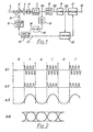
- an embodiment of the present invention has a local oscillator light source 5, a half- mirror 2 for so multiplexing a local oscillator light beam 6 and a modulated arriving light beam 1 that their wave fronts coincide with each other, a germanium photodiode 4 for receiving the multiplexed light beam and converting it into an electric signal of an intermediate frequency, and a lens 3 for focusing the light beam on said photodiode.
- This embodiment further has an intermediate frequency amplifier 7, an intermediate frequency extractor 13, a frequency divider 14 and a synchronous controller 15, which, together with the local oscillator light source 5, the photodiode 4 and so on, constitute a phase locked loop.
- the output of the intermediate frequency amplifier 7 is supplied to an envelope detector 8, and the detected output is fed to a baseband amplifier 9 with a built-in lowpass filter.
- the output of the baseband amplifier 9 is supplied to a timing circuit 10, where a clock frequency component is extracted and a timing pulse is generated. With this timing pulse serving as the trigger, a regenerator circuit 11 regenerates the original signal from the output of the baseband amplifier 9.
- the timing pulse from the timing extraction circuit 10 is also fed to the local oscillator control circuit 15.
- Ge-PD germanium photodiode
- an InGaAsP semiconductor laser 5 which is the local oscillator light source, is supplied the local oscillator light wave 6, whose frequency is 128 MHz lower than that of the optical carrier 1, and this local oscillator light wave 6 is multiplexed with the optical carrier 1 by the half-mirror 2, the multiplexed light being focused by the lens 3 and entered into the Ge-PD 4.
- the optical carrier land the local oscillator light wave 6 are so adjusted on the light receiving surface of the Ge-PD 4 that their directions of polarization, wave fronts and so forth coincide with each other, and this Ge-PD 4 achieves the mixing for optical heterodyne detection.
- an intermediate frequency signal of 128 MHz, pulse amplitude-modulated at 32 Mb/s as a result of the mixing.
- This signal after being amplified by the intermediate frequency amplifier 7, is envelope-detected by the envelope detector 8, and further undergoes amplification, band limitation and so forth by the baseband amplifier 9, from which is fed a signal to the timing circuit 10, where a sine wave of 32 MHz is extracted and on its basis is generated a timing pulse of 32 Mb/s.
- the 32 MHz sine wave is supplied to the local oscillator control circouit 15, while the 32 Mb/s timing pulse is fed to the regenerator circuit 11.
- the output signal of the amplifier 9 enters the regenerator circuit 11, is regenerated under synchronization by the timing pulse from the timing circuit 10, and supplied to an output terminal.
- the output signal of the intermediate frequency amplifier 7 is bisected, and one part is entered into the envelope detector 8, while the other is fed to the intermediate frequency extractor 13 to undergo the extraction of a 128 MHz intermediate frequency.
- the driving current of the InGaAsP semiconductor laser 5 is slightly reduced and its oscillating frequency raised.
- the oscillating frequency of the InGaAsP semiconductor laser 5 is too high, its driving current is slightly raised and its oscillating frequency lowered.
- the intermediate frequency is synchronized with the quadruple of the 32 MHz repeating frequency of the pulse signal.
- the eightfold of the half cycle of the intermediate frequency is synchronized with the full cycle of the repeating frequency of the pulse signal.
- (al) is the output waveform of the intermediate frequency amplifier 7; (a2), that of the envelope detector 8; (a3), that of the amplifier 9; and (a4), the eye pattern of the output of the amplifier 9. Since the 128 MHz intermediate frequency is in synchronism with the 32 MHz repeating frequency of the pulse signal, .both the output waveform (a2) of the envelope detector 8 and that (a3) of the amplifier 9 are free from distortion. Accordingly, the eye pattern (a4) of the output of the amplifier 9 manifests a satisfactory waveform, almost completely free from jitter. Regeneration of the output of this amplifier 9, therefore, results in satisfactory pulse regeneration.
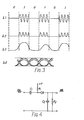
- the intermediate frequency and the repeating frequency of the pulse signal are not synchronized with each other, i.e. the intermediate frequency extractor 13, the 1/4 frequency divider 14 and the synchronous controller 15 of the foregoing embodiment are absent, with reference to FIG. 3, wherein the output waveforms bl, b2 and b3 of the intermediate frequency amplifier 7, the envelope detector 8 and the baseband amplifier 9, respectively, are shown, toegether with an eye pattern b4.
- the repeating frequency of the pulse signal is 32 MHz like in the foregoing embodiment, the intermediate frequency is 107 MHz.
- the phase of the input waveform (bl) of the intermediate frequency amplifier 7 differs from one pulse to another.
- the output waveforms (b2) and (b3) of the envelope detector 8 and the amplifier 9, respectively vary from pulse to pulse. Therefore, conspicuous jitters emerge in the eye pattern (b4) of the output of the amplifier 9.
- the optical receiver sensitivity deteriorates by at least 3 dB on account of the jitters.
- a distributed feedback type buried heterostructure can be used as the InGaAsP semiconductor laser, which is the local oscillator light source 5.
- This laser oscillates in a single axial mode and in a single lateral mode. Varying the driving current by 0.1 mA would result in the variation of the oscillating frequency by about 100 MHz. Therefore, if a control signal actually deviates to 130 MHz from the desired intermediate frequency of 128 MHz, the driving current of this semiconductor will have to be reduced by approximately 0.002 mA to adjust the intermediate frequency to 128 MHz.
- the envelope detector circuit 8 also is well known in the art, and can consist, for instance, mainly of a diode and RC circuits as illustrated in FIG. 4.
- the timing circuit 10 and the regenerator circuit 11, too, are well known in PCM technology or digital technology.
- the timing circuit 10 extracts a timing component from the output signal of the baseband amplifier 9, and generates a sine wave of 32 MHz and a timing pulse signal of 32 Mb/s, a pulsified product of the sine wave.
- the band is narrowed with a monolithic crystal filter to remove noise, other than the linear spectrum, from the baseband signal and thereby to generate the sine wave, in which jitters are suppresed, and this sine wave is further supplied to a pulser to generate . the timing pulse signal.
- the regenerator circuit 11 discriminates, according to the timing signal from the timing circuit 10, whether the output signal from the baseband amplifier 9 is "1" or "0", and regenerates it into a pulse signal.
- the intermediate frequency extractor circuit 13 is intended for extracting an intermediate frequency component from an intermediate frequency signal, amplitude-modulated at 32 Mb/s, and involves an intermediate frequency filter having a center frequency of 128 MHz.
- the sine wave of the intermediate frequency is generated herein, and converted into a pulse signal of this frequency.
- the frequency divider 14 divides by 1/4 the frequency of the pulse signal supplied from the intermediate frequency extractor circuit 13 to convert it into a sine singal, which is then supplied to the local oscillator control circuit 15.
- the local oscillator control circuit 15 primarily comprising a phase comparator circuit, a lowpass filter and a level controller, adjusts at its output level the current of the driving circuit for the local oscillator light source 5.
- the phase comparator circuit compares the sine wave signal 17, corresponding to the bit rate of the pulse amplitude modulation, supplied from the timing circuit 10, and the phase of the sine wave, resulting from the 1/4 frequency division of the intermediate frequency, supplied from the frequency divider 14, and generates an average D.C. voltage proportional to the difference between them.
- This voltage after passing the lowpass filter, is fed to the driving circuit of the semiconductor laser for local oscillation through the level controller, resulting in the control of the driving current to vary the oscillation frequency. Therefore, the semiconductor laser 5, photodiode 4, intermediate frequency amplifier 7, intermediate frequency extractor 13, frequency divider 14, local oscillator control circuit 15, and leads and light paths connecting them together constitute a phase locked loop.
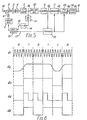
- FIG. 5 is a block diagram illustrating the structure of a second preferred embodiment of the present invention
- FIG. 6 shows signal waveforms in various parts of this embodiment.
- From an InGaAsP semiconductor laser 5 is supplied a local oscillator light wave 6, whose frequency is 128 MHz lower than that of the optical carrier 21, and the optical carrier 21 and the local oscillator light wave 6 are mixed and optically heterodyne-detected by the Ge-PD 4.
- the delay detector 22 intended for converting binarily phase-modulated signals into binarily amplitude-modulated signals, is well known in the art as a phase modulation detector. To be more specific, it branches into two signals a binarily phase-modulated input signal, so delays each branched signal with a delay circuit as to be delayed by a single-bit equivalent (31.25 ns) and feeds it to a double balanced mixer, which figures out the difference between the two branched signals, and converts the binarily phase-modulated intermediate frequency signal into a binarily amplitude-modulated baseband signal.
- the output signal of the delay detector 22 further undergoes amplification, band limitation and the like by a baseband amplifier 9, which gives an output signal d2.
- This output signal d2 of the amplifier 9 is supplied to a timing extractor 30, which extracts a timing signal of 32 MHz to generate a timing pulse of 32 Mbits, and supplies timing signals to a regenerator 11 and a pulse width share converter 23.
- the output signal of the regenerator 11 enters the pulse width share converter 23, and is converted into a pulse signal of R Z code.
- the pulse width share converter circuit 23 figures out the logical sum of the regeneration signal d3 from the regenerator circuit 11 and the timing pulse supplied from the timing extractor circuit 30, and punches the signal pulse with the timing pulse to convert the signal pulse into a pulse signal d4 of 50% in duty ratio.
- a code converter 24 reverses the code of the output pulse at each leading edge of the input pulse to regenerate the original binary pulse signal d5, which is fed to an output terminal 12.
- This code converter 24 can consist of a flipflop.
- composition and operation of all other sections of this second preferred embodiment are the same as the respectively corresponding sections of the first embodiment. Since the intermediate frequency of 128 MHz is synchronized with the repeating frequency of the pulse signal in this embodiment like in the first, satisfactory waveforms which are almost completely free from distortion have been obtained from its amplifier 9.
- the two frequencies may be of different values as long as the Nth integer (N may be any positive integer, though it is an even number in the first embodiment) of the half cycle of the intermediate frequency are synchronized with the full cycle of the pulse signal.
- N may be any positive integer, though it is an even number in the first embodiment
- a binary NRZ code is used for the pulse signal herein, it may have some other code, such as a binary RZ code, code mark inversion (CMI) code, differential mark inversion (DMI) code or mBnB code.
- the pulse share converter 23 and the code converter 24, if they are contained in the light transmitter section and their effects therefore already included in the optical carrier 21, can be dispensed with.
- a frequency quadrupler may be inserted between the timing extractor 10 or 30 and the local oscillator control circuit 15 and synchronization be achieved at 128 MHz in the local oscillator control circuit 15.
Abstract
Description
- The present invention relates to a pulse receiving system and method for use in the receiver section of a pulse communication system, and more particularly to a pulse receiving system and method using heterodyne detection in an optical wave band or the like.
- The optical heterodyne detection technique, by which optical signals are detected by a heterodyne procedure, gains the advantage of permitting substantial improvement of the optical receiver sensitivity over the direct optical detection technique. According to this optical heterodyne detection method, the signal light which is a modulated carrier having a high frequency of several hundreds of THz and the local oscillator light having substantially the same frequency are mixed by an optical detector to be converted into an electric signal having an intermediate frequency in the VHF band or the microwave band, and then this signal is demodulated into the original electric signal.
- Previously, where the demodulated electric signal was a pulse signal, the intermediate frequency had to be set sufficiently high, no less than 15 times as high as the repeating frequency of the pulse signal. There, was the disadvantage that, unless the intermediate frequency was high enough, a waveform distortion would arise, with the amplitude, width and phase of the pulse differing from one pulse to another, resulting in a deterioration of optical receiver sensitivity.
- However, a high intermediate frequency would necessitate an intermediate frequency amplifier in the high frequency band. This would entail a greater cost and a higher level of thermal noise, requiring a high level of local oscillator. If the level of the local oscillator light was low, the optical receiver sensitivity would deteriorate. Therefore, it is desirable to set the intermediate frequency low without inviting pulse waveform distortion.
- An object of the present invention, accordingly, is to provide an optical heterodyne detection pulse receiving method and system capable of setting the intermediate frequency low, no more than one-third of what is used for the same purpose in prior art, without inviting pulse waveform distortion.
- According to the invention, there is provided an optical heterodyne detection pulse receiving method whereby a local oscillator light wave and an optical carrier, modulated with a pulse signal, are mixed; a signal having an intermediate frequency equal to the difference between the frequency of the local oscillator light wave and that of the optical carrier is extracted; and the pulse signal is regenerated by demodulating this intermediate frequency signal, characterized in that an integral multiple of the half cycle of the intermediate frequency is synchronized with the full cycle of the repeating frequency of the pulse signal.
- In the optical heterodyne detection pulse receiving method according to the invention, the full cycle of the repeating frequency of the demodulated pulse signal is N synchronized with an integral multiple/of the half cycle of the intermediate frequency.
- Where the optical carrier modulated with a pulse signal is a pulse amplitude-modulated optical carrier, if a half- wave rectifying envelope detector is used for demodulating an intermediate frequency signal to regenerate the pulse signal, N has to be a positive even number, but if a whole- wave rectifying detector is used for that purpose, N merely has to be a positive integer, either odd or even.
- Where the optical carrier modulated with a pulse signal is a pulse phase-modulated optical carrier, again N only has to be a positive integer, either odd or even.
- Therefore, even if the intermediate frequency is set as low as four to six times the repeating frequency of the demodulated pulse signal, there will be no waveform distortion, wherein the amplitude, width and phase of the demodulated pulse signal differ from one pulse to another, and consequently no deterioration of optical receiver sensitivity. Since the pulse receiving method according to the invention permits the intermediate frequency to be set as low as about one-third to a quarter of what is used for the same purpose in prior art, the receiver section can be less expensively constructed, and the local oscillator wave can be less powerful.
-
- FIG. 1 is a block diagram illustrating a first preferred embodiment of the present invention;
- FIG. 2 is a timing chart referring to various sections of said first embodiment of the invention;
- FIG. 3 is a timing chart of waveforms obtained where the present invention is not used;
- FIG. 4 is a circuit diagram of an envelope detector for use in the first embodiment of the invention;
- FIG. 5 is a block diagram illustrating a second preferred embodiment of the invention; and
- FIG. 6 is a timing chart referring to various sections of the second embodiment of the invention.
- Referring to FIG. 1, an embodiment of the present invention has a local
oscillator light source 5, a half-mirror 2 for so multiplexing a local oscillator light beam 6 and a modulated arrivinglight beam 1 that their wave fronts coincide with each other, agermanium photodiode 4 for receiving the multiplexed light beam and converting it into an electric signal of an intermediate frequency, and alens 3 for focusing the light beam on said photodiode. This embodiment further has anintermediate frequency amplifier 7, anintermediate frequency extractor 13, afrequency divider 14 and asynchronous controller 15, which, together with the localoscillator light source 5, thephotodiode 4 and so on, constitute a phase locked loop. The output of theintermediate frequency amplifier 7 is supplied to an envelope detector 8, and the detected output is fed to abaseband amplifier 9 with a built-in lowpass filter. The output of thebaseband amplifier 9 is supplied to atiming circuit 10, where a clock frequency component is extracted and a timing pulse is generated. With this timing pulse serving as the trigger, aregenerator circuit 11 regenerates the original signal from the output of thebaseband amplifier 9. The timing pulse from thetiming extraction circuit 10 is also fed to the localoscillator control circuit 15. - The optical carrier of 230.77 kHz in frequency (or 1.3 µm in wavelength), pulse amplitude-modulated at a bit rate of 32 Mb/s, passes the
halfmirror 2, is focused by thelens 3 and enters the germanium photodiode (Ge-PD) 4, which is an optical detector. Meanwhile, from an InGaAsPsemiconductor laser 5, which is the local oscillator light source, is supplied the local oscillator light wave 6, whose frequency is 128 MHz lower than that of theoptical carrier 1, and this local oscillator light wave 6 is multiplexed with theoptical carrier 1 by the half-mirror 2, the multiplexed light being focused by thelens 3 and entered into the Ge-PD 4. The optical carrier land the local oscillator light wave 6 are so adjusted on the light receiving surface of the Ge-PD 4 that their directions of polarization, wave fronts and so forth coincide with each other, and this Ge-PD 4 achieves the mixing for optical heterodyne detection. From the Ge-PD 4 is supplied an intermediate frequency signal of 128 MHz, pulse amplitude-modulated at 32 Mb/s as a result of the mixing. This signal, after being amplified by theintermediate frequency amplifier 7, is envelope-detected by the envelope detector 8, and further undergoes amplification, band limitation and so forth by thebaseband amplifier 9, from which is fed a signal to thetiming circuit 10, where a sine wave of 32 MHz is extracted and on its basis is generated a timing pulse of 32 Mb/s. The 32 MHz sine wave is supplied to the local oscillator control circouit 15, while the 32 Mb/s timing pulse is fed to theregenerator circuit 11. The output signal of theamplifier 9 enters theregenerator circuit 11, is regenerated under synchronization by the timing pulse from thetiming circuit 10, and supplied to an output terminal. - The output signal of the
intermediate frequency amplifier 7 is bisected, and one part is entered into the envelope detector 8, while the other is fed to theintermediate frequency extractor 13 to undergo the extraction of a 128 MHz intermediate frequency. The output of theintermediate frequency extractor 13, after being converted into a 32 MHz frequency by the 1/4frequency divider 14, becomes afirst input signal 16 to the localoscillator control circuit 15, which compares thefirst input signal 16 and asecond input signal 17 supplied from thetiming circuit 10, and so controls the driving current of the InGaAsPsemiconductor laser 5, which is the local oscillator light source, as to synchronize the two input signals. Thus, if the oscillating frequency of theInGaAsP semiconductor laser 5 is too low to keep the intermediate frequency no higher than 128 MHz and allows the frequency of thefirst input signal 16 to be higher than the 32 MHz frequency of thesecond input signal 17, the driving current of theInGaAsP semiconductor laser 5 is slightly reduced and its oscillating frequency raised. Or if, conversely, the oscillating frequency of the InGaAsPsemiconductor laser 5 is too high, its driving current is slightly raised and its oscillating frequency lowered. - By this control procedure, the intermediate frequency is synchronized with the quadruple of the 32 MHz repeating frequency of the pulse signal. Thus, the eightfold of the half cycle of the intermediate frequency is synchronized with the full cycle of the repeating frequency of the pulse signal.
- In FIG. 2, (al) is the output waveform of the
intermediate frequency amplifier 7; (a2), that of the envelope detector 8; (a3), that of theamplifier 9; and (a4), the eye pattern of the output of theamplifier 9. Since the 128 MHz intermediate frequency is in synchronism with the 32 MHz repeating frequency of the pulse signal, .both the output waveform (a2) of the envelope detector 8 and that (a3) of theamplifier 9 are free from distortion. Accordingly, the eye pattern (a4) of the output of theamplifier 9 manifests a satisfactory waveform, almost completely free from jitter. Regeneration of the output of thisamplifier 9, therefore, results in satisfactory pulse regeneration. - To describe the advantage of the foregoing embodiment in further detail, cited below is an instance in which the intermediate frequency and the repeating frequency of the pulse signal are not synchronized with each other, i.e. the
intermediate frequency extractor 13, the 1/4frequency divider 14 and thesynchronous controller 15 of the foregoing embodiment are absent, with reference to FIG. 3, wherein the output waveforms bl, b2 and b3 of theintermediate frequency amplifier 7, the envelope detector 8 and thebaseband amplifier 9, respectively, are shown, toegether with an eye pattern b4. In this case, although the repeating frequency of the pulse signal is 32 MHz like in the foregoing embodiment, the intermediate frequency is 107 MHz. Because no integral multiple of the full cycle of the intermediate frequency is identical with the full cycle of the pulse signal, the phase of the input waveform (bl) of theintermediate frequency amplifier 7 differs from one pulse to another. As a result, there are such distortions that the output waveforms (b2) and (b3) of the envelope detector 8 and theamplifier 9, respectively, vary from pulse to pulse. Therefore, conspicuous jitters emerge in the eye pattern (b4) of the output of theamplifier 9. In this instance, compared with the foregoing embodiment, the optical receiver sensitivity deteriorates by at least 3 dB on account of the jitters. - Next will be described the individual elements used in this preferred embodiment of the present invention.
- A distributed feedback type buried heterostructure can be used as the InGaAsP semiconductor laser, which is the local
oscillator light source 5. This laser oscillates in a single axial mode and in a single lateral mode. Varying the driving current by 0.1 mA would result in the variation of the oscillating frequency by about 100 MHz. Therefore, if a control signal actually deviates to 130 MHz from the desired intermediate frequency of 128 MHz, the driving current of this semiconductor will have to be reduced by approximately 0.002 mA to adjust the intermediate frequency to 128 MHz. - The envelope detector circuit 8 also is well known in the art, and can consist, for instance, mainly of a diode and RC circuits as illustrated in FIG. 4. In this particular embodiment, C1 is a pass condenser of 0.1 to 1 µF; R1 is for bias supply, several kQ, and C2R2 is selected at a time constant substantially equal to the cycle of the intermediate frequency, acceptable at
C 2 = 10 pF and R2 R2 = 800 Ω. - The
timing circuit 10 and theregenerator circuit 11, too, are well known in PCM technology or digital technology. In a brief description, thetiming circuit 10 extracts a timing component from the output signal of thebaseband amplifier 9, and generates a sine wave of 32 MHz and a timing pulse signal of 32 Mb/s, a pulsified product of the sine wave. For example, the band is narrowed with a monolithic crystal filter to remove noise, other than the linear spectrum, from the baseband signal and thereby to generate the sine wave, in which jitters are suppresed, and this sine wave is further supplied to a pulser to generate . the timing pulse signal. Theregenerator circuit 11 discriminates, according to the timing signal from thetiming circuit 10, whether the output signal from thebaseband amplifier 9 is "1" or "0", and regenerates it into a pulse signal. - The intermediate
frequency extractor circuit 13 is intended for extracting an intermediate frequency component from an intermediate frequency signal, amplitude-modulated at 32 Mb/s, and involves an intermediate frequency filter having a center frequency of 128 MHz. The sine wave of the intermediate frequency is generated herein, and converted into a pulse signal of this frequency. - The
frequency divider 14 divides by 1/4 the frequency of the pulse signal supplied from the intermediatefrequency extractor circuit 13 to convert it into a sine singal, which is then supplied to the localoscillator control circuit 15. - The local
oscillator control circuit 15, primarily comprising a phase comparator circuit, a lowpass filter and a level controller, adjusts at its output level the current of the driving circuit for the localoscillator light source 5. The phase comparator circuit compares thesine wave signal 17, corresponding to the bit rate of the pulse amplitude modulation, supplied from thetiming circuit 10, and the phase of the sine wave, resulting from the 1/4 frequency division of the intermediate frequency, supplied from thefrequency divider 14, and generates an average D.C. voltage proportional to the difference between them. This voltage, after passing the lowpass filter, is fed to the driving circuit of the semiconductor laser for local oscillation through the level controller, resulting in the control of the driving current to vary the oscillation frequency. Therefore, thesemiconductor laser 5,photodiode 4,intermediate frequency amplifier 7,intermediate frequency extractor 13,frequency divider 14, localoscillator control circuit 15, and leads and light paths connecting them together constitute a phase locked loop. - FIG. 5 is a block diagram illustrating the structure of a second preferred embodiment of the present invention, and FIG. 6 shows signal waveforms in various parts of this embodiment. An optical carrier of 230.77 THz in frequency (or 1.3 µm in wavelength), pulse phase-modulated with a pulse signal of 32 Mb/s in bit rate, passes a
halfmirror 2, and is focused by alens 3 to enter a Ge-PD 4. From anInGaAsP semiconductor laser 5 is supplied a local oscillator light wave 6, whose frequency is 128 MHz lower than that of theoptical carrier 21, and theoptical carrier 21 and the local oscillator light wave 6 are mixed and optically heterodyne-detected by the Ge-PD 4. From the Ge-PD 4 is supplied an intermediate frequency signal of 128 MHz, pulse phase-modulated at 32 Mb/s, and after this signal is amplified by anintermediate frequency amplifier 7, its output signal dl is delay-detected by adelay detector 22 to be converted into a binary pulse signal of 32 Mb/s. - The
delay detector 22, intended for converting binarily phase-modulated signals into binarily amplitude-modulated signals, is well known in the art as a phase modulation detector. To be more specific, it branches into two signals a binarily phase-modulated input signal, so delays each branched signal with a delay circuit as to be delayed by a single-bit equivalent (31.25 ns) and feeds it to a double balanced mixer, which figures out the difference between the two branched signals, and converts the binarily phase-modulated intermediate frequency signal into a binarily amplitude-modulated baseband signal. The output signal of thedelay detector 22 further undergoes amplification, band limitation and the like by abaseband amplifier 9, which gives an output signal d2. This output signal d2 of theamplifier 9 is supplied to a timing extractor 30, which extracts a timing signal of 32 MHz to generate a timing pulse of 32 Mbits, and supplies timing signals to aregenerator 11 and a pulsewidth share converter 23. The output signal of theamplifier 9 enters theregenerator 11, is synchronized by a timing signal of 32 Mbits and regenerated as a regeneration signal d3. - The output signal of the
regenerator 11 enters the pulsewidth share converter 23, and is converted into a pulse signal of RZ code. The pulse widthshare converter circuit 23 figures out the logical sum of the regeneration signal d3 from theregenerator circuit 11 and the timing pulse supplied from the timing extractor circuit 30, and punches the signal pulse with the timing pulse to convert the signal pulse into a pulse signal d4 of 50% in duty ratio. Acode converter 24 reverses the code of the output pulse at each leading edge of the input pulse to regenerate the original binary pulse signal d5, which is fed to anoutput terminal 12. Thiscode converter 24 can consist of a flipflop. - The composition and operation of all other sections of this second preferred embodiment are the same as the respectively corresponding sections of the first embodiment. Since the intermediate frequency of 128 MHz is synchronized with the repeating frequency of the pulse signal in this embodiment like in the first, satisfactory waveforms which are almost completely free from distortion have been obtained from its
amplifier 9. - Although an intermediate frequency of 128 MHz and a pulse signal bit rate of 32 Mbits are used in both of the foregoing preferred embodiments, the two frequencies may be of different values as long as the Nth integer (N may be any positive integer, though it is an even number in the first embodiment) of the half cycle of the intermediate frequency are synchronized with the full cycle of the pulse signal. Though a binary NRZ code is used for the pulse signal herein, it may have some other code, such as a binary RZ code, code mark inversion (CMI) code, differential mark inversion (DMI) code or mBnB code. In the second embodiment, the
pulse share converter 23 and thecode converter 24, if they are contained in the light transmitter section and their effects therefore already included in theoptical carrier 21, can be dispensed with. Instead of using the 1/4frequency divider 14 like in the two foregoing embodiments, a frequency quadrupler may be inserted between the timingextractor 10 or 30 and the localoscillator control circuit 15 and synchronization be achieved at 128 MHz in the localoscillator control circuit 15.
Claims (7)
Applications Claiming Priority (2)
| Application Number | Priority Date | Filing Date | Title |
|---|---|---|---|
| JP58014201A JPS59140736A (en) | 1983-01-31 | 1983-01-31 | Optical heterodyne detection pulse receiving method |
| JP14201/83 | 1983-01-31 |
Publications (2)
| Publication Number | Publication Date |
|---|---|
| EP0115445A2 true EP0115445A2 (en) | 1984-08-08 |
| EP0115445A3 EP0115445A3 (en) | 1988-05-11 |
Family
ID=11854494
Family Applications (1)
| Application Number | Title | Priority Date | Filing Date |
|---|---|---|---|
| EP84300603A Ceased EP0115445A3 (en) | 1983-01-31 | 1984-01-31 | Optical heterodyne detection pulse receiving system and method |
Country Status (4)
| Country | Link |
|---|---|
| US (1) | US4706300A (en) |
| EP (1) | EP0115445A3 (en) |
| JP (1) | JPS59140736A (en) |
| CA (1) | CA1215120A (en) |
Cited By (2)
| Publication number | Priority date | Publication date | Assignee | Title |
|---|---|---|---|---|
| US4775972A (en) * | 1985-05-10 | 1988-10-04 | Itt Corporation, Defense Communications Division | Optical fiber communication for local area networks with frequency-division-multiplexing |
| GB2213014A (en) * | 1987-11-30 | 1989-08-02 | Plessey Telecomm | Control circuit for the local oscillator of an optical homodyne or heterodyne receiver of a phase shift keying system |
Families Citing this family (13)
| Publication number | Priority date | Publication date | Assignee | Title |
|---|---|---|---|---|
| US4893353A (en) * | 1985-12-20 | 1990-01-09 | Yokogawa Electric Corporation | Optical frequency synthesizer/sweeper |
| US4794351A (en) * | 1986-09-29 | 1988-12-27 | American Telephone And Telegraph Company, At&T Bell Laboratories | Optical mixer for upconverting or downconverting an optical signal |
| US4824201A (en) * | 1987-07-13 | 1989-04-25 | Bell Communications Research, Inc. | Simultaneous transmission of LED and laser signals over single mode fiber |
| US4945229A (en) * | 1988-12-29 | 1990-07-31 | Thomas & Betts Corporation | Fiber optic receiver and transceiver |
| US5548434A (en) * | 1993-12-01 | 1996-08-20 | Sharp Kabushiki Kaisha | Spatial light transmission apparatus |
| JP3846918B2 (en) * | 1994-08-02 | 2006-11-15 | 富士通株式会社 | Optical transmission system, optical multiplex transmission system and related technologies |
| US20050046482A1 (en) * | 2003-08-27 | 2005-03-03 | Karl Schrodinger | Receiver circuit |
| US7561813B2 (en) * | 2005-06-09 | 2009-07-14 | Northrop Grumman Corporation | Wide field of view heterodyne receiver |
| JP4213172B2 (en) * | 2006-06-19 | 2009-01-21 | 日本電波工業株式会社 | PLL oscillator circuit |
| US8787774B2 (en) * | 2007-10-10 | 2014-07-22 | Luxtera, Inc. | Method and system for a narrowband, non-linear optoelectronic receiver |
| KR101503534B1 (en) * | 2008-11-28 | 2015-03-17 | 삼성전자주식회사 | Apparatus for transmiting and receving visible light communication data |
| CN112640329A (en) * | 2018-09-07 | 2021-04-09 | 日本电气株式会社 | Optical receiver and receiving method |
| JP2021129167A (en) * | 2020-02-12 | 2021-09-02 | 日本電気株式会社 | Optical radio transmission system |
Citations (2)
| Publication number | Priority date | Publication date | Assignee | Title |
|---|---|---|---|---|
| US3482099A (en) * | 1965-08-16 | 1969-12-02 | Hughes Aircraft Co | Tuned stable laser in a communication system |
| US3899772A (en) * | 1973-04-23 | 1975-08-12 | Kustom Electronics | Mobile computer terminal and system |
Family Cites Families (6)
| Publication number | Priority date | Publication date | Assignee | Title |
|---|---|---|---|---|
| US3426207A (en) * | 1964-06-17 | 1969-02-04 | North American Rockwell | Focused optical heterodyne system |
| US3530298A (en) * | 1968-04-17 | 1970-09-22 | Bell Telephone Labor Inc | Optical heterodyne receiver with pulse widening or stretching |
| US3939341A (en) * | 1975-04-02 | 1976-02-17 | Hughes Aircraft Company | Phase-locked optical homodyne receiver |
| US3975628A (en) * | 1975-04-02 | 1976-08-17 | Hughes Aircraft Company | Optical heterodyne receiver with phase or frequency lock |
| JPS6013567B2 (en) * | 1978-03-30 | 1985-04-08 | ソニー株式会社 | television receiver |
| JPS56150734A (en) * | 1980-04-23 | 1981-11-21 | Nippon Telegr & Teleph Corp <Ntt> | Heterodyne receiver for optical communication using semiconductor laser |
-
1983
- 1983-01-31 JP JP58014201A patent/JPS59140736A/en active Pending
-
1984
- 1984-01-30 CA CA000446357A patent/CA1215120A/en not_active Expired
- 1984-01-31 US US06/575,595 patent/US4706300A/en not_active Expired - Lifetime
- 1984-01-31 EP EP84300603A patent/EP0115445A3/en not_active Ceased
Patent Citations (2)
| Publication number | Priority date | Publication date | Assignee | Title |
|---|---|---|---|---|
| US3482099A (en) * | 1965-08-16 | 1969-12-02 | Hughes Aircraft Co | Tuned stable laser in a communication system |
| US3899772A (en) * | 1973-04-23 | 1975-08-12 | Kustom Electronics | Mobile computer terminal and system |
Non-Patent Citations (2)
| Title |
|---|
| 7TH EUROPEAN CONFERENCE ON OPTICAL COMMUNICATION, CONFERENCE PROCEEDINGS, Copenhagen, 8th-11th September 1981, pages 17.1.1 - 17.1.3, Peregrinus Ltd, London, GB; F. FAVRE et al.: "Future heterodyne-type single mode fibre communication systems" * |
| PATENT ABSTRACTS OF JAPAN, vol. 4, no. 165 (E-34)[647], 15th November 1980; & JP-A-55 112 060 (NIPPON DENKI K.K.) 29-08-1980 * |
Cited By (2)
| Publication number | Priority date | Publication date | Assignee | Title |
|---|---|---|---|---|
| US4775972A (en) * | 1985-05-10 | 1988-10-04 | Itt Corporation, Defense Communications Division | Optical fiber communication for local area networks with frequency-division-multiplexing |
| GB2213014A (en) * | 1987-11-30 | 1989-08-02 | Plessey Telecomm | Control circuit for the local oscillator of an optical homodyne or heterodyne receiver of a phase shift keying system |
Also Published As
| Publication number | Publication date |
|---|---|
| CA1215120A (en) | 1986-12-09 |
| JPS59140736A (en) | 1984-08-13 |
| EP0115445A3 (en) | 1988-05-11 |
| US4706300A (en) | 1987-11-10 |
Similar Documents
| Publication | Publication Date | Title |
|---|---|---|
| US3956626A (en) | Pulse quaternary communication means | |
| US4706300A (en) | Optical heterodyne detection pulse receiving system and method | |
| US4965858A (en) | Polarization diversity optical receiver for coherent optical communication | |
| US5894247A (en) | Optical PLL circuit and method of controlling the same | |
| US4142155A (en) | Diversity system | |
| JP3173788B2 (en) | Digital transmission equipment and direct conversion receiver | |
| US4980891A (en) | Clocked optical regenerator and other optoelectronic functional circuits | |
| EP1134917B1 (en) | Generating methods for single and multi-channel wideband optical analog pulse positioned waveforms | |
| US6323991B2 (en) | Opto-electronic frequency divider circuit and method of operating same | |
| US4737968A (en) | QPSK transmission system having phaselocked tracking filter for spectrum shaping | |
| US6282007B1 (en) | Optical timing detection | |
| US6509990B1 (en) | Optical timing detection | |
| US6775482B1 (en) | Light receiver | |
| JPH10150417A (en) | Optical receiver and automatic frequency detection clock extract circuit used for it | |
| US6549598B1 (en) | Clock signal extraction circuit | |
| US5077754A (en) | Tau-dither circuit | |
| US3946148A (en) | Television receiver operable in exact or extended range tuning modes | |
| US6542723B1 (en) | Optoelectronic phase locked loop with balanced photodetection for clock recovery in high-speed optical time division multiplexed systems | |
| EP0064728A2 (en) | Multiple phase digital modulator | |
| US5046140A (en) | Automatic optical frequency acquisition and tracking apparatus for optical coherent communication system | |
| US5272559A (en) | Truncated frequency discriminator | |
| US3502985A (en) | Regenerative repeater and phase regenerating circuit | |
| JP2606191B2 (en) | Optical heterodyne synchronous detector | |
| JP3219063B2 (en) | Phase synchronization control device and phase synchronization control method | |
| WO2006046435A1 (en) | Optical/electric clock signal extraction device |
Legal Events
| Date | Code | Title | Description |
|---|---|---|---|
| PUAI | Public reference made under article 153(3) epc to a published international application that has entered the european phase |
Free format text: ORIGINAL CODE: 0009012 |
|
| 17P | Request for examination filed |
Effective date: 19840208 |
|
| AK | Designated contracting states |
Designated state(s): DE FR GB |
|
| PUAL | Search report despatched |
Free format text: ORIGINAL CODE: 0009013 |
|
| AK | Designated contracting states |
Kind code of ref document: A3 Designated state(s): DE FR GB |
|
| STAA | Information on the status of an ep patent application or granted ep patent |
Free format text: STATUS: EXAMINATION IS IN PROGRESS |
|
| 17Q | First examination report despatched |
Effective date: 19890630 |
|
| 18R | Application refused |
Effective date: 19900129 |
|
| RIN1 | Information on inventor provided before grant (corrected) |
Inventor name: MINEMURA, KOUICHI Inventor name: SHIKADA, MINORU Inventor name: EMURA, KATSUMI |