EP0111792B1 - Device for processing non-associated signalization for an automatic tdm switching system - Google Patents
Device for processing non-associated signalization for an automatic tdm switching system Download PDFInfo
- Publication number
- EP0111792B1 EP0111792B1 EP83112070A EP83112070A EP0111792B1 EP 0111792 B1 EP0111792 B1 EP 0111792B1 EP 83112070 A EP83112070 A EP 83112070A EP 83112070 A EP83112070 A EP 83112070A EP 0111792 B1 EP0111792 B1 EP 0111792B1
- Authority
- EP
- European Patent Office
- Prior art keywords
- circuit
- multiplex
- memory
- signal
- signalisation
- Prior art date
- Legal status (The legal status is an assumption and is not a legal conclusion. Google has not performed a legal analysis and makes no representation as to the accuracy of the status listed.)
- Expired
Links
Images


Classifications
-
- H—ELECTRICITY
- H04—ELECTRIC COMMUNICATION TECHNIQUE
- H04Q—SELECTING
- H04Q11/00—Selecting arrangements for multiplex systems
- H04Q11/04—Selecting arrangements for multiplex systems for time-division multiplexing
- H04Q11/0407—Selecting arrangements for multiplex systems for time-division multiplexing using a stored programme control
Definitions
- the invention relates to a device for processing signaling channel by channel in a time switch. It is applicable in particular in a telephone exchange comprising digital lines operated in call-by-call mode and digital lines operated in reserved mode.
- connection network In such a central, it is usual to connect an input line or circuit to an output line or circuit by means of the connection network, the signaling being received and transmitted under the control of the control members of the central.
- connection network In the case of reserved lines, it is not possible, as in the old analog systems, to directly connect the incoming line to the outgoing line in a permanent manner during the rental period of the line.
- Semi-permanent connections are therefore established in the connection network for the reserved lines, and the signaling received in the same manner as for the lines operated on a call-by-call basis, is retransmitted at the output of the connection network so that the central is transparent for reserved lines, and that the lessor has complete freedom to use the signaling channel assigned to him.
- the object of the invention is to provide a device carrying out processing of the signaling of the channels in call by call, and a simple switching of the signaling for the reserved lines, in a PABX comprising in particular microprocessor control units , microprocessor terminal units and a connection network, such as the automatic switch mentioned in French patent application 2 503 513 by the applicant.
- control and terminal units are connected to the connection network by two-way multiplex links ensuring communication between the terminal units on the one hand, for establishing communications, and on the other hand with the control units which control them; the terminal units include digital circuit terminal units which serve to service the MIC time junctions.
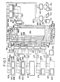
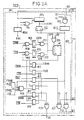
- the time switch shown in Figure 1 includes a time connection network RCX, microprocessor control units UC, UCP and terminal units UT.
- the RCX time switching network is preferably of the type described in French patent application n ° 2,503,514 by the applicant, it includes independent switching plans referenced RXA to RXD which each include several time switches each controlled by a marker MQ, such as MQD1, the MQ markers of a plan being generally referenced MQA, MQB, MQC or MQD in FIG. 1.
- the PABX control system is preferably of the type described in French patent application No. 2 503 513 of the applicant, it is made up of standardized UC control units, here grouped into GUC groups of q units of which only one GUC1 has been shown here, as well as UCP peripheral control units, here f.
- Each control unit UC essentially comprises a microprocessor linked by bus links to memories and to specialized link interfaces.
- UCP peripheral control units have almost the same structure as standard UC control units, they do differentiate in particular by the fact that they include specialized couplers, not shown here, for specific peripherals, such as couplers for a disc PF1 and a dialogue terminal PF2 in the case of the peripheral control unit UCP1 and couplers in a magnetic tape dispenser PF3 and for an operator terminal PF4 for the device control unit UCPf.
- a network RIT of duplicate point-to-point links RIT1, RIT2, managed by duplicate distributors DR1, DR2 connects the control units UC, the control units for peripheral devices UCP and the markers MO for their exchanges of information.
- a general time base BTG provides the clock and synchronization signals necessary for the operation of the automatic exchange, it is for example of the type described in French patent application No. 2,390,856 and then comprises three unrepresented oscillators which provide the clock and synchronization signals in the form of three pairs of two signals, one of the clock and the other of synchronization.
- the general time base BTG supplies the control units UC and the terminal units UT with clock and synchronization signals via distribution modules MD and clock and synchronization circuits CBT.
- each distribution module MD such as MDA1
- MDA is associated with a time switch and supervised by the marker MQ controlling this time switch, the distribution modules associated with a plan being here referenced MDA, MDB, MDC or MDD.
- Each clock and synchronization circuit CBT receives the clock and synchronization signals supplied by two distribution modules MD, via time base links generally referenced LBT, in order to make these signals available to the control units UC d a GUC group or UT terminal units of a determined GUT group, it being understood that the UT terminal units are also grouped by GUT groups comprising at least one and generally several terminal units.
- Each clock and synchronization circuit is also interposed for synchronization purposes on multiplex links generally referenced MU which connect the terminal units of a GUT group or the control units of a GUC group to the RCX connection network. , for message exchanges between units, each GUC or GUT group being connected to each RX plane of the connection network by a different MU multiplex link.
- Each multiple link MU is bidirectional and comprises for example thirty-two eight-bit channels allowing a bit rate of two megabits / second in each direction of transmission.
- the multiplex links MU and the time base links LBT serving a group GUC or GUT are combined into two beams of identical constitution generally referenced F1 and F2 upstream of the clock and synchronization circuit CBT serving this group and LC1, LC2 downstream of this circuit on the unit side, each unit of the group being connected to each of the two beams LC1, LC2, which therefore each comprise two multiplex links MU and a time base link LBT, since they are the continuation one of a beam F1, the other of a beam F2.
- the exchanges between the terminal units UT and the control units UC are carried out by means of messages in semaphore procedure, for example of the HDLC type, which use the multiplex links MU via time channels which are switched by the network of RCX connection.
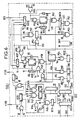
- FIG. 2 makes it possible to specify the constitution of a digital circuit terminal unit UTI or UTJ and its links with the clock and synchronization circuit CBT which serves it.
- Each clock and synchronization circuit is composed of two duplicated half-circuits CBT1, CBT2 connected one to a beam F1, the other to a beam F2 and one serving a beam LC1, the other a beam LC2 .
- the two multiplex links MU of a bundle F each break down into a so-called incoming network link LRE and into a so-called outgoing network link LRS, which are associated with a time base link LBT comprising a clock distribution wire and a weft synchronization wire, not shown, to form this beam F, such as LRE1, LRS1, LRE2, LRS2, LBT1 for the beam F1.
- Each half-circuit CBT1, CBT2 of a clock and synchronization circuit produces the clock and synchronization signals necessary for a group of units, by means of a conventional time base, not shown, which receives clock signals coming from a distribution module MD via a time base link LBT, these signals are transmitted to all the units of a group by a link of clock and synchronization signals HS, such as HS1 of the beam LC1 for the terminal unit UT presented in Figure 2.
- Each half-circuit CBT1, CBT2 also includes conventional synchronization circuits, not shown, for phasing the LRE, LRS network links to which it is connected with internal LTE incoming and LTS outgoing multiplex links which serve all the terminal units in parallel. of a GUT group.
- a terminal unit UTI usually comprises a microprocessor mPl, a random access memory MV1 and a read-only memory MM1, a time connection matrix CX1 and its control circuit CQ1, a transceiver ER1 allowing the microprocessor mP1 to transmit and receive messages in HDLC procedure via LTE9, LTS9 multiplex links connected to the CX1 connection network, a programmable CRS1 monitoring counter, a PIC1 circuit for taking account of interruptions intended for the mP1 microprocessor, a CN digital circuit.
- the digital circuit CN comprises a digital terminal TN for a bidirectional MIC time junction MI composed of a transmitted link MICE and a received link MICR, a synchronization and signaling circuit SES for the signaling to be transmitted and a reception circuit for GIS signaling for channel-by-channel signaling carried by the IT16 time channels of the MICR time link.
- the microprocessor mP1 of a digital circuit terminal unit UTI is connected by an address bus BA1, a data bus BD1 and a control bus BK1, to the memories MM1, MV1, to the control circuit CQ1, to the counter of CRS1 monitoring, PIC1 recognition circuit, ER1 transceiver, as well as TN terminal and SES, SIG signaling circuits of the CN digital circuit.
- the TN terminal and the SES, SIG signaling circuits of a digital terminal unit UTI are also connected to the time connection matrix CX1 of the unit by internal incoming and outgoing multiplex links LTE, LTS, as well as the ER1 transceiver.
- the TN terminal provides on the one hand the interface between the received time link MICR and an outgoing multiplex link LTS8 and on the other hand the interface between an incoming multiplex link LTE8 and the transmitted time link MICE, it includes for this purpose circuits specific to one or other of the directions of transmission and a common circuit for choosing clock and synchronization signals CHS.
- the choice circuit CHS of a digital circuit terminal unit UTI ensures the selection, under the control of the unit's microprocessor mP1, of the signals transmitted by one of the two clock and synchronization signal links HS1 and HS2 to which the unit is connected.
- a rest code generation circuit ECR is connected to an outgoing multiplex link LTS7 for the purpose of transmitting a rest code on the unused channels on the order of the microprocessor mP1 of the terminal unit UTI which comprises it, at rhythm fixed by the clock and synchronization signals transmitted by the CHS choice circuit.
- the transmission between the incoming LTE multiplex link and the received time link MICR implements a frame synchronization signal injection circuit SS inserted with the incoming multiplex link LTE8 at the input of a CD transcoder which supplies the transmitted time link MICE with signals in HDB3 code from the binary signals received.
- the synchronization and signaling circuit SES essentially comprises a multiframe synchronization analysis device Sm connected by its input to an incoming multiplex link LTE5, a synchronization circuit RB connected to the multiframe synchronization circuit SM and to the incoming multiplex link and ensuring the resynchronization of the signals coming from the mixing unit UTB with respect to the local multiframe signal and a signaling transmission circuit ES connected to the synchronization circuit RB and connected by its output to an outgoing multiplex link LTS5.
- the signaling reception circuit SIG which is also connected to two multiplex links, one incoming LTE6, the other outgoing LTS6, ensures the reception of the signaling reaching channel sixteen on the received time link MICR, via the link LTS8 and the CX1 time connection network.
- the signaling circuits SIG and SES of a digital terminal unit UTI are also connected at the output of the choice circuit CHS from which they receive the signals and to the buses BA1, BD1, BK1 of the microprocessor mP1 as well as the digital terminal TN.
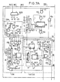
- FIG. 3 makes it possible to specify the constitution of a UTB mixing unit and its LTE, LTS, HS links with the clock and synchronization circuit CBT which serves the group to which this UTB unit belongs.
- the LTE, LTS, HS links are identical to those described in relation to the digital terminal unit UTI, and where the clock and synchronization circuit CBT is also, these links and this circuit will appear with the same references and will not be redefined, with some exceptions.
- the GUTB group of UTB patch units has the same general structure as a group of UTI digital circuit terminal units.
- a patching unit UTB essentially comprises a microprocessor mP2, a random access memory MV2, a read-only memory MM2, a time connection matrix CX2 and its control circuit CQ2, a transceiver ER2 allowing the microprocessor mP2 to transmit and receive in HDLC procedure via LE2, LS2 links connected to the CX2 connection network, a programmable CRS2 monitoring counter, a PIC2 circuit for taking into account the interruption for the mP2 microprocessor, a BR mixer and its CRB control circuit. an address bus BA2, a data bus BD2 and a control bus BK2.
- a cross-connect BR is intended to serve a number j of digital circuits CN, corresponding for example to thirty two circuits, ie 960 telephone channels.
- the RCX connection network switches the time channels of rank sixteen carrying the signaling of the reserved channels of the j digital circuits CN served by a cross-connect BR to j paths of the multiplex links MU, serving the group.
- GUTB of UTB brewing units which contains the BR brewer in question.
- LIE incoming multiplex link
- a BR stirrer is capable of brewing 960 signaling quartets.
- the cross-connect BR also manages multi-frame synchronization, because if the signaling channels coming from the various digital circuits CN have been synchronized at the level of the frame, the position of the frame alignment signal is arbitrary at the input of the cross-connect BR.
- Cross-connection is carried out using a cross-connection buffer memory MT connected to the incoming multiplex link LIE by a series-parallel conversion circuit CSP.
- the MT shuffle memory contains one-byte words.
- the memory is read in nibbles and the bytes to be transmitted are composed by an injection circuit INJ connected to the outgoing multiplex link LIS by a parallel-serial converter CPS.
- a sequencer SQ receives the signals from the HS links and distributes the channel addressing signals synchronous with the reference signal mentioned above, as well as signals s1 to sn for sequencing the internal operation of the cross-connect BR.
- the shuffle orders are written by the microprocessor mP2 in a control memory MC addressed in writing by the address bus BA2 and in reading by the sequencer SQ, via a multiplexer MX11 in both cases.
- the processing of the multiframe locking signals is carried out by an AUT controller connected to the incoming multiplex link LIE and to a multiframe shift circuit CDM.
- FIGS. 4 to 7 make it possible to specify the circuits involved in implementing the present invention, it should be noted that in the following description, a door is optionally called a set of identical elementary doors controlled identically.
- the digital terminal TN detailed in FIG. 4 comprises a decoder DEC1 connected to the microprocessor mP1 of the terminal unit UTI which comprises this terminal, via the address bus BA1 and the control bus BK1.
- the decoder DEC1 supplies validation signals V1 to V4, a write signal VE1 and read signals VL1 to VL4.
- the choice circuit CHS comprises a multiplexer MX1 connected by its inputs to the clock and synchronization signal links HS1, HS2, it delivers a clock signal W and its complement W via an inverter 10 to the frequency of 2048 kilohertz in the application presented, as well as a frame synchronization signal SY and a multiframe synchronization signal SMT.
- This multiplexer MX1 is addressed by a flip-flop B1 controlled by a gate P1, of type ET, which receives a validation signal V1 from the decoder DEC1 and an indication of choice of link HS by the microprocessor mP1 of the terminal unit via the bus. BD1 data.
- the transcoder TR supplies transcoded binary signals LME and a remote clock signal WD, from the signals in HDB3 code supplied by the received time link MICR.
- Frame synchronization is carried out by a standard synchronization circuit ST1, such as for example the circuit SM300 from the company Siemens, this circuit ST1 provides binary signals synchronized on its output SO from the signals received on its input LME connected to the transcoder TR .
- a standard synchronization circuit ST1 such as for example the circuit SM300 from the company Siemens, this circuit ST1 provides binary signals synchronized on its output SO from the signals received on its input LME connected to the transcoder TR .
- the synchronization circuit ST1 is arranged to monitor the differences between the remote clock WD and the local clock W which is supplied to it in complemented form W at one of its inputs SC, it performs the jumps or doubling of the necessary frame.
- An output SP of the synchronization circuit ST1 indicates the detection of a frame alignment signal among the signals received from the transcoder TR; in the event of non-recognition of this frame alignment signal, a pulse is supplied by the output FP of the circuit ST1 and the output SO is maintained at state 1, so as to produce a characteristic signal of loss of alignment in favor of the circuits downstream.
- two flip-flops B2 and B3 and an inverter 11 give a signal of loss of frame alignment PVT which causes, via a flip-flop B4, an interrupt request IN1 to the circuit for taking into account the interruption PIC1 of the UTI terminal unit, and which sets an alarm bit in a locking signal sent on the time link sent MICE, as shown later.
- the nature of the alarm is indicated at an output DB of the synchronization circuit ST1 which is read by the microprocessor mP1 of the terminal unit UTI.
- a generator G validated by a validation signal V2, emits a pulse on the input PE of the synchronization circuit ST1 and to an input of a gate P4 of type ET which is also connected to the output DB and which receives an RW signal.
- Gate P4 supplies a register RE1, the output of which is connected to bus BD1 via a gate P5.
- Gate P5 connects the register RE1 to the bus BD1 on reception of a read validation signal VL1.
- the changes of state of the output SP of the synchronization circuit SP1 are compatibilized by a counter CTE connected at the output of flip-flop B3 by a gate P6 of type ET validated by the pulse emitted at the output FP of the circuit ST1.
- the counter CTE is read by the microprocessor mP1 via the data bus BD1 and a gate P7 of type ET validated by a validation signal VL2.
- the output SO of the module ST1 which supplies the signals emanating from the time link received MICR after transcoding and resynchronization, is connected to the input of a register RE2 whose output gives access to the outgoing multiplex link LTS8 by a flip-flop B5.
- the locking word sent on this link LTS8 can be read by the microprocessor mP1 of the terminal unit UTI, for this it is loaded into a register RE3 connected via a gate P8 of type ET at the output of the register RE2 in parallel with the rocker B5.
- the instant of the loading controlled via the gate P8 is fixed by a synchronization device connected to one of the inputs of this gate P8, it is determined by the synchronization signal SY applied to a flip-flop B7 whose output feeds a shift register RD1, the output of which is connected to the above-mentioned input of gate P8.
- a loss of synchronization on the received time link MICR is signaled by the appearance of a succession of bits of value one at the output of this link.
- the condition fixed to trigger an alarm is that there are less than eight bits in the zero state in a frame, this is controlled using a shift register RD2 connected to the LME and WD links coming from the transcoder TR via a door P10 of type ET and a rocker B8.
- This RD2 register is read by the microprocessor mP1 of the terminal unit UTI via a gate P11 of ET type whose output is connected to the data bus BD1, one input of which receives a read validation signal VL3 and the other input of which receives the signal from the register shift RD2, via an inverter 12 in series with a flip-flop B9 connected by its inputs at the output of register RD2 and flip-flop B7.
- the VTO frame alignment signal is transmitted over the transmitted time link MICE to the input of the CD transcoder using an ET type P12 gate receiving the VTO signal on one input and the signals originating from the incoming multiplex link. LTE8 on a second input.
- the microprocessor mP1 controls the generation of binary signals of value one during the time of injection of the VTO signal, while during the time corresponding to the passage of the other channels, it is the terminal itself which maintains the VTO signal. at level one.
- the signal VTO is supplied at the output of a register RD3 which receives the signals for locking the VTP even frame or the VTI odd frame emanating from a multiplexer MX2, via a gate P14 of the ET type which has another input connected at the output of the register RD1 via an AND type gate P13 and a flip-flop B10, the gate P13 being controlled by the clock signal W and the flip-flop B10 by its complement W.
- Bits two through eight of the VTP even frame alignment signal are wired (K), the bit of this signal and the eight bits of the odd VTI frame alignment signal are supplied by the UTI terminal unit's microprocessor mP1 via the data bus BD1, a gate P15 validated by a write signal VE1 and a register RE4 connected to the multiplexer MX2.
- This multiplexer MX2 is controlled by the synchronization signal SY via an inverter 13 and a flip-flop B6, the output of which is also connected to an input SCT of the synchronization circuit ST1 via a gate PO of type ET whose other input receives the signal SY.
- Bit three of the odd frame alignment signal VTI can also be set to one by the digital terminal TN via an OR type P16 gate connected to an input of the multiplexer MX2, in the event of loss of frame alignment.
- the gate P16 receives on the one hand the frame lock loss signal supplied by the inverter 11, it is connected on the other hand at the output of the register RE4.
- a rest code is permanently transmitted on the outgoing multiplex link LTS7 by a conventional ECR circuit controlled by the signals SY and W so as to occupy the time channels unused by the digital terminal TAB.
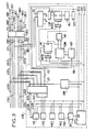
- the synchronization and signaling circuit SES presented in FIG. 5 essentially comprises, as described above, a multiframe synchronization search device SM, a synchronization circuit RD of the crossover signal BR with respect to the local multiframe signal and an ES signaling transmission circuit.
- This SES synchronization and signaling circuit makes it possible to process supermultitrames of four frames, making it possible to increase the number of signaling channels in signaling channel sixteen. Indeed, with a normal frame, a channel bit sixteen of a frame corresponds to a channel at 512 Hz, while with the supermultitrame mentioned above, a channel bit sixteen of a frame makes it possible to obtain a channel of 512 Hz, two channels at 256 Hz or four channels at 128 Hz for a multiframe. Multiframe synchronization is sought successively for the channel signals coming from a time link received MICR and for the channel signals coming from a cross-connect BR. For this, the time connection matrix CX1 switches the signaling coming from the time link received MICR on channel thirty-one of the incoming multiplex link LTE5 and the signaling reserved on channel fifteen of this same link LTE5.
- the synchronization and signaling circuit SES uses, on the one hand, addressing signals Aj, validation in write EC and in read LEC supplied by a decoder DEC2 connected to the address buses BA1 and control BK1 associated with the microprocessor mP1, on the other hand clock signals W of frame synchronization SY and of multiframe SMT supplied by the clock choice and synchronization circuit CHS that the digital terminal TN associated with this circuit SES comprises in the same terminal unit UTI .
- the internal operating phases of the synchronization and signaling circuit SES are determined by a binary counter CR1 controlled by the clock signal W and synchronized by the multiframe synchronization signal SMT via a set of gates P17, P18, P19, P43 of the ET type and an inverter 13 duly combined.
- the binary counter CR1 has fourteen bits making it possible to identify, using three bits CO to C2, a bit number, using five bits C3 to C7, a time channel number and using four bits C8 at C11 a frame number in a multiframe identified itself in a superframe by two bits C12, C13.
- the bits CO to C11 are loaded at an initial value K1 and the bits C12 and C13 are reloaded via the gate P19 so as not to lose the multiframe numbers.
- the operating phases of the synchronization and signaling circuit are obtained either directly on the outputs of the counter CR1. either via a logic circuit with gates CLP1, moreover if the phase must be synchronized with a clock signal edge W, a group of flip-flops GB1 controlled by this clock signal W is also used, this group GB1 also provides a transmission clock signal HE.
- the multiframe synchronization analysis device SM consists of a lock memory M1 of the REPROM type which here comprises 4 K eight-bit words, the state of the multi-frame lock VMT being represented by eight bits.
- the first four referenced 0 to 3 allow a frame count, when a VMT multiframe locking is detected, these four bits are at zero and indicate the first frame in zero frame of the multiframe, later this counting indicates the rank and the weft processed.
- the fifth bit referenced 4 is intended to signal the non-recognition of the locking word in a first multiframe frame.
- the sixth bit referenced 5 is intended to signal that the byte received is composed of zeros, it is updated with each frame whatever the locking status and it is used for the detection of time value zero bits signaling IT16 during one or two successive multiframes and when the multiframe locking signal is resumed to indicate that the previous IT16 time channel has been received with at least one bit of value one.
- the seventh bit referenced 6 indicates the loss of PVMT multiframe locking after reception of two erroneous multiframe interlocks.
- the eighth bit referenced 7 indicates processing of the last multiframe frame.
- the first seven multiframe locking signal bits are stored in a status register RES for processing the signaling emanating from the received time link MICR and in a status register RE6 for the signaling received from the cross-connect BR.
- the status registers RES and RE6 are connected at the output of the lock memory M1 via respectively a gate P20 for the status register RES5 and a gate P22 for the status register RE6, the gate P20 is validated by the LDMR complement of the LDMR multiframe locking search signal and the gate P22 is validated by the LDB complement of the LDB multiframe locking search signal.
- the multiframe locking search signals LDMR and LDB selectively ensure the validation of the locking memory M1, via a gate P24 of the OR type to the inputs of which they are applied and the selective validation of gates P21 and P23 placed at the output l one from the status register RES, the other from the status register RE6, and connected to the addressing inputs of the locking memory M1.
- the microprocessor mP1 of the terminal unit UTI controls the transmission of the signaling to the synchronization and signaling circuit SES at the desired times so as to allow storage in the signaling register RD4.
- the two quartets transmitted during the time interval IT16 of the seventeenth channel of the received time link MICR are memorized during the time interval IT31 of the last frame channel under the control of the signal DEMR applied to the input of the RD4 register via an OR type PO gate.
- the processing of the two quartets coming from the received time link MICR is ensured during the time interval IT14 of the fifteenth channel so as to store under the control of the signal LDMR in lock memory M1 the two bits 7 and 8 supplied by the zero state decoder DEZ, this LDMR signal being applied to the P24 gate of the OR type.
- the two quartets sent by a brewer BR are received by the register RD4 during the time interval IT15 of the sixteenth channel under the control of the signal DEB applied to the gate PO and the two corresponding bits 7 and 8 supplied by the decoder DEZ zero state are stored from locking M1 under the control of the signal LDB during the time interval IT30 corresponding to the penultimate frame channel.
- the multiframe locking VMT is considered to be lost when two locking signals are successively received in error.
- the multiframe locking VMT is sought in the second frame TP1 and in the penultimate frame TR15 to ensure that there has not been a doubling or frame jump at the input of the digital terminal TN, before the loss of multiframe locking is reported.
- Multiframe locking is also considered lost when all the bits of the signaling channel are in the zero state for a period corresponding to one or two frames.
- Multiframe locking is considered to be resumed upon detection of at least one bit in state one in the channel time interval IT16 which precedes the first detected multiframe locking signal.
- a group of six flip-flops of information B11 to B16 makes it possible to memorize the passage of the last frame of a multiframe and to give the alarm to the microprocessor mP1 by sending an interrupt IN4, the flip-flops B11, B12, B15 and B16 are selectively connected at the output of the lock memory M1 by their inputs and all of the six flip-flops are controlled in the manner described below.
- the flip-flops B11 and B12 respectively supply signals T15MR and T15B of the last multiframe frame for the received time link MICR and the cross-connect BR respectively, these signals correspond to the content of bits 7 in lock memory M1 and the flip-flops are respectively validated by the LDMR and LDB complements LDMR and LDB multiframe locking search signals.
- the flip-flops B15 and B16 respectively provide multiframe locking loss signals for the received time link MICR and the cross-connect BR respectively, these signals correspond to the content of bits 6 in the locking memory M1 and the flip-flops are validated respectively by the LDMR complements and LDB of the obtained LDMR and LDB multiframe locking signals.
- the flip-flop B13 provides a remote alarm indication SIAL following the detection, by a logic detection circuit DEAL, of alarm information transmitted by the multiplex link LTE5 to which the detection circuit DEAL is connected.
- the flip-flop B13 which receives the output signal from the detection circuit DEAL via an inverter 110 is validated by the signal T15MR supplied by the flip-flop B11.
- the flip-flop B14 provides an indication relating to a loss of remote locking indicated by bit 6 at the output of signaling register RD4, it is connected to the corresponding output of this register by a gate P25 of type ET validated simultaneously by the signal of last frame T15MR at the flip-flop output B11, the multiframe locking signal LDMR, the frame locking loss signal PVMT supplied by the rank bit 6 at the output of the signaling register RD4 and a signal C3 supplied by the counter CR1.
- the outputs of flip-flops B13 to B15 are connected to a gate P26 of the OR type supplying an interrupt signal IN4 intended for the circuit for taking into account the interrupt P1C1 of the microprocessor MP1.
- This microprocessor MP1 has the ability to read the outputs of flip-flops B12 to B16 via a multiple door P27 and type ET whose unit doors are validated by the read signal LEC and address information AI supplied by the DEC2 decoder.
- the orders here consist of sixteen bits split into two bytes, one of least significant and the other of most significant.
- the least significant byte and the first four bits of the most significant byte here correspond to the signaling transmission time
- the fifth bit or bit 4 corresponds to the state of the bit in transmission
- the sixth bit is masked and indicates when it is zero that the channel is reserved for signals from the brewer.
- the seventh bit indicates an interrupt to be reported and the eighth bit indicates the state of the bit to be transmitted taking into account the mask and the cross-connect.
- the input into the send memory M2 is controlled by a gate P38 of type ET which receives the signals supplied for a multiplexer MX3 and a validation signal which is the complement of the signal LM of general validation of output which the group of flip-flops provides.
- a gate P38 of type ET which receives the signals supplied for a multiplexer MX3 and a validation signal which is the complement of the signal LM of general validation of output which the group of flip-flops provides.
- GB1 to a gate P28 of type ET which controls the output of the send memory MT2, the signal LM being complemented by an inverter 114 before being applied to the gate P38.
- the multiplexer MX4 the selection of the inputs of which is controlled by a mask bit 13 contained in the register RES, comprises two inputs one connected to the output of the shift register RD5 the other receiving a bit 12 of the register RES.
- the multiplexer MX5 is cyclically controlled by the counting signals supplied by the counter CR1, which addresses the send memory M2 every four channel time intervals to constitute an eight-bit word intended to be transmitted in the IT16 signaling channel on the MICE time link transmitted served by the UTI terminal unit considered.
- the duration of transmission of a signaling is fixed by the down-counter DES which receives the twelve bits intended for this use.
- two gates P29 and P30 share the distribution of the twelve bits at the down-counter DES, they are inserted at the output of another gate P28 also of type ET which is connected at the output of memory M2 and are respectively controlled one by the LDFA read signal and the other by the other LDFO read signal.
- the DES down-counter is decremented if bit 11 which is the transmission duration weight bit is in state one, corresponding to a transmission command of limited duration, if it is in transmission zero state is cyclical to each multiframe for a period not limited by counting.
- the RES register stores bits 4 to 7 of the most significant byte.
- the modified data contained in the down-counter DES and the register RES are introduced into the sending memory M2 at the same address as the data which gave them birth, the counter CR1 having kept the outputs C5 to C13 in the same state.
- the send memory M2 is addressed by the counter CR3 controlled by the clock signal H2 applied to a gate P36 controlled by the complement of the last frame signal T15B which is supplied by a inverter 113, the counter CR3 is synchronized by the last frame signal T15B applied to a gate P37 with the clock signal HE and a wired indication K6.
- the information emanating from the cross-connector BR is received by the shift register RD5 connected by its input to the incoming multiplex link LTE5 and controlled by the signal DEB supplied by the logic unit CLP1.
- the reading of the sending memory M2 is controlled either by a bit Ci at the output of the counter CRi, or by the signal LEC emanating from the microprocessor mP1, both being applied to a gate P39 of the OR type whose output is connected to an input of gate P28 of the ET type which is connected to the output of send memory M2 and which is controlled by the signal LM.
- a logic circuit LO formed of flip-flops not shown, is connected to the outputs of the down-counter DES and of the register RES, it makes it possible to transmit an interrupt IN3 towards the circuit for taking into account the interruption CIP1 of the microprocessor mP1 at the end of transmission 'a signaling bit.
- the logic circuit LO also makes it possible to trigger the loading of the register RES in a buffer register RE8 via a gate P32 of type ET as well as the introduction of the address Aj concerned in a register RE9 via a gate P33 of type ET.
- the registers RE8 and RE9 and the send memory M2 are read by the microprocessor mP1 via the data bus BD1 and respectively each of the gates P34, P35, P40 of type ET controlled by the read signal LEC and an address Aj, door P40 being inserted downstream of door P28.
- a command register RE10 is connected by its inputs to a gate P41 of type ET which receives data emanating from the microprocessor mP1 via the bus BD1, this gate P41 being controlled by the write signal and an address Ai.
- the RE10 command register is linked by its outputs to the memory M1 for testing purposes, to a reset input for the alarm flip-flops B13 to B16 and to the bus BD1 via a gate P42 of the ET type similarly controlled. at gate P40.
- a door P27 of type ET makes it possible to connect the flip-flops B13 to B16 to the microprocessor mP1 via the bus BD1 data for reading.
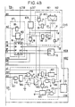
- the signaling reception circuit SIG presented in FIG. 6 receives the signaling transmitted on channel sixteen of the received time link MICR, on the switch of the microprocessor mP1 and via the incoming multiplex link LTE6, it detects changes in the status of bits of signaling and transmission of confirmed changes to the mP1 microprocessor.
- a decoder DEC3 connects the circuit SIG to the address buses BA1 and of control BK1 and deduces therefrom a write signal EC, a write signal LEC and address signals generally referenced Ak.
- a counter CR4 of the twelve-bit type ensures the internal synchronization of the signaling reception circuit SIG from the clock signals W and the multiframe synchronization SMT which it receives from the choice circuit CHS belonging to the same terminal unit UTI.
- a logic unit with doors CLP2 and a group of flip-flops for phasing GB 2 ensure the adaptation of the synchronization signals to the needs of the signaling reception circuit SIG, they are connected for this purpose to the synchronization counter CR4, and the logic unit CLP2 which controls the group of flip-flops GB2 is connected to the decoder DEC3.
- the synchronization counter CR4 has its clock input activated by the clock signals W in the absence of a multiframe synchronization signal SMT of value one, this being achieved by using a gate P46 of type ET receiving the signal SMT via an inverter 115 and the signal W.
- the SMT signal for the first eight bits of the counter CR4 and the last frame signal T15MR supplied by the synchronization and signaling circuit SES for the last four bits ensure, the synchronization of the meter via doors P47 and P48 of type ET receiving one the signal W, the signal SMT and a wired indication K3, the other the signal W, the signal T15MR and a wired indication K4.
- the signaling coming from the channel corresponding to the interval IT16 of the received time link MICR, via the incoming multiplex link LTE6, for a reserved line is on the one hand transmitted to a receiver shift register RD6, on the other hand to a transmitter shift register RD7 via an OR type P40 gate, the output of this transmitter register RD7 supplying the outgoing multiplex link LTS6.
- the command input of the receiver register RD6 is controlled by a gate P50 of type ET which receives the complement W of the clock signal and one of the validation signals Vi supplied by the logic unit CLP2, the command input of the register transmitter RD7 also receives the complement W of the clock signal supplied by the clock selection circuit CHS.
- the receiver register RD6 has its bit outputs 5 and 7 connected to a register RE7 which stores the super-multiframe number as defined by these bits 5 and 7, a gate P49 of type ET is inserted for this purpose between the registers RD6 and RE7 , it is controlled by the clock signal W and the last frame signal T15MR transmitted by the group of flip-flops GB2.
- the output of the superframe number register RE7 is connected to an input of the logic unit CLP2, so as to allow access to the signals transmitted by low bit rate channels distributed over two or four multiframes.
- this change of state is written to a state memory M3 used in the FIFO stack (first in-first out) which can be read by the microprocessor mP1 of the UTI unit.
- the state memory M3 is addressed through a multiplexer MX6 either by the microprocessor mP1 providing an address Ak, or by a counter CRS.
- the multiplexer being controlled by a signal Vi coming from the logic unit CLP2.
- a new state is deduced from the previous state in the following manner, firstly simultaneously the storage memory M4 and the receiver register RD6 respectively produce the sixteen bits of two words relating to a signaling bit via a gate P59 of type ET and the corresponding new signaling bit nbs.
- bit nbs and the five bits 11 to 15 are applied to the address inputs of the translation memory M5 which supplies in response a word of six bits, this word is loaded into a buffer register RE12 via a gate P54, of type ET , controlled by a signal VSi from the group of flip-flops GB2.
- Simultaneously bits 0 to 11 are applied to the inputs of a counter CR6 via doors P60, P61 of the ET type controlled respectively by two signals VSi supplied by the group of flip-flops GB2 under the control of the counter CK7.
- the CR6 counter is incremented by the CR4 counter via the group of flip-flops GB2.
- the twelve bits contained in the counter CR6 and four of the six bits provided by the translation memory M5 are applied to the input of the storage memory M4 via a gate P56 of type ET whose inputs are connected at the output of a multiplexer MX7 which is controlled by a signal Vi supplied by the logic unit CLP2.
- the multiplexer MX7 is connected by a second group of inputs to the data bus BD1 so as to allow the execution of tests, the gate P56 is for its part controlled via a gate P55 of the OR type or by the write signal EC either by a signal Vsi supplied by the group of flip-flops GB2.
- the storage memory M4 is addressed either by the logic unit CLP2 by means of a signal Vi, or by an address Ak sent by the microprocessor mP1, via the address bus BA1, the signal Vi and l address Ak being both applied to a multiplexer MX8, driven by another signal Vi of the logic unit CLP2.
- the gate P59 at the output of the storage memory M4 supplies the beveler CR6, the translation memory M5 and a multiplexer MX9, it is controlled on the one hand by the output signal from the gate P55 supplemented by an inverter 116 and on the other on the one hand by an OR type P58 gate receiving on the one hand a signal Vi coming from the logic unit CLP2 on the other hand another signal Vi coming from this same unit combined with the signal LEC by means of a gate P57 of the type AND.
- a confirmed change of state is indicated by the state one of the most significant bit referenced ce of the word read in translation memory M5, this bit loaded in the register RE12 is supplied to an activation input of a multiplexer MX10 placed at the input of the state memory M3, so as to allow the loading of the contents of the register RE12 and the counter CR6 there.
- the multiplexer MX10 is controlled by a signal Vi emanating from the logic unit CLP2 and by an address Ak supplied by the microprocessor mP1 via the address address BAi.
- the multiplexer MX10 is connected by its inputs to the data bus BD1, at the output of the multiplexer MX8 for addressing the storage memory M4, at the output of the register RE12 and at the output of the counter CR6.
- the connection of the multiplexer MX10 to the data bus BD1 allows the test of the state memory M3, the connection of the multiplexer MX10 at the output of the multiplexer MX8 allows the introduction into state memory of the identification number of the signaling bit at which corresponds to the change of state.
- a gate P64 of type ET is inserted between the multiplexer MX10 and the state memory M3, it is controlled via a gate P65 of type OR either by the write signal EC or by a signal Vsi emanating from the group of flip-flops GB2.
- a gate P63 of the AND type is inserted at the output of the state memory M3 upstream of the multiplexer MX9; it is controlled by a signal Vi emanating from the logic unit CLP2, by the read signal LEC and by the complement of the output signal. of the P65 gate which controls the writing in state memory, as supplied by an inverter 118.
- the multiplexer MX9 which is connected as seen at the output of gate P59 for reading memory storage M4 and at the output of gate P63 for reading state memory M3 is connected to the data bus BD1 via a gate P62 of ET type controlled by the read signal LEC and an address Ak supplied by the decoder DEC3 which also controls the multiplexer MX9 by two other addresses Ak.
- the bit ce also causes the counter CR6 to be reset to zero and it ensures the progression of the counter CR5 via a gate P51 of the ET type controlled by a signal Vsi from the group of flip-flops GB2.
- the counter CR5 is connected by its prepositioning inputs to the data bus BD1 via a gate P52 of the ET type which is controlled by the write signal EC and by an address Ak of the decoder DEC3.
- the counter CR5 which is connected by its outputs to the multiplexer MX6 is also connected to the data bus BD1 via a gate P53 of the AND type controlled by the read signal LEC and an address Ak.
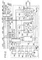
- the cross-connect BR presented in FIG. 7 comprises a decoder DEC5 supplying address address Ai, write EC and read LEC from information received from the microprocessor mP2 of the cross-connection unit UTB comprising it, via a bus d BA2 address and a BK2 control bus which connect them.
- the cross-connector BR also receives the clock signal W and its complement W, a clock signal WR phase shifted by a quarter of a period with respect to the signal W, the multiframe synchronization signal SMT and its complement SMT, of a circuit not shown which is equivalent to the clock selection circuit CHS and which is identically connected to the clock and synchronization signal links HS1 and HS2 of a circuit CBT.
- An SQ sequencer organized around a CR7 counter makes it possible to adjust the succession of operations to be performed on each channel.
- the counter CR7 which has twelve bit outputs CO to C11 is controlled by the clock signal W and synchronized by the signal SMT which is supplied to it via an input of a gate P70 of ET type whose other input is prepositioned to a K5 value by wiring.
- the bits CO to C2 supplied by the first three outputs of the counter CR7 are applied to a decoder DEC4 which supplies eight sequencing signals in the form of bits s1 to s8 for the sequence of operations during eight successive clock times; the first half of the operating cycle on a channel defined by the provision of times s1 to s4 and the presence of a bit C4 of value zero is reserved for dialogue with the microprocessor mP2.
- a group of flip-flops GB3 connected to the outputs of the decoder DEC4 and controlled by the clock signal W provides synchronized validation signals VSj.
- the crossover buffer memory MT has its access controlled by a parallel series conversion circuit CSP connected by its input to the incoming internal link LIE.
- This CSP circuit consists of an RD8 shift input register connected downstream of the incoming internal LIE link and controlled by the signal complementary to clock W and a buffer register RE13 which receives in parallel the eight bits of a signaling channel transmitted by the link LIE via the input register RD8 and a gate P71 of type ET validated via a gate P72 of NAND type which receives signals s1 and WR.
- This MT cross-connection memory is carried out by means of a multiplexer MX12 connected on the one hand to the bit outputs C3 to C11 of the counter CR7 which define a channel in a multiframe frame, on the other hand at the output of control memory MC by a link NA and at the output of a buffer register RE16 by a link NC of a memory which will be defined below, the alternative selection of the inputs of the multiplexer MX12 being ensured by the bit C2 which provides it with the CR7 counter on its corresponding output.
- the injection circuit INJ placed downstream of the shuffling memory MT includes access doors P75, P76 of type ET for the quartets to be brewed, these doors connected upstream to two groups of quartet outputs of the shuffling memory MT are selectively and additionally validated by the output signals of a multiplexer MX13 connected directly to an input of gate P75 and via an inverter 117 to gate P76.
- the multiplexer MX13 is addressed by the bit outputs s2 and s3 of the decoder DEC4 and it has three inputs, the first of which is connected to the control memory output MC of the cross-connector CB, the second of which is fixed at zero and the third fixed at level a.
- the outputs of the gates 75 and 76 control a quartet generation memory M6 of the PROM type, via a P77 gate of the OR type, in connection with the bits a12 to a15 which define the parameters of the codes used and which are supplied by the memory of MC command.
- the parallel-serial conversion circuit placed at the memory output M6 receives the two quartets intended to constitute a byte in two buffer registers RE14, RE15 via gates P78.
- P79 of ET type which are controlled by the complementary clock signal W and on the one hand the output signal s6 of the decoder DEC4 for the gate P78 and on the other hand the output signal s7 of this decoder for the gate P79.
- the outputs of the buffer registers RE14, RE15 are connected to a shift transmission register RD9 via a gate P80 of ET type which is controlled by the complementary clock signal W and the sequencing signal s8 of the decoder DEC4.
- the transmission register which receives the bits of the quartets in parallel ensures their transmission in series on the internal transmission link LIS, under the control of a gate P81 of type ET which receives the complementary clock signal W and a signal supplied by an inverter 118 inserted downstream of the output s8.
- the control memory MC of cross-connect BR is of RAM type, it contains the shuffle orders and it is connected for this purpose by its inputs to the data bus BD2, of the microprocessor mP2, via two doors P82, P83 of type ET in series , which are respectively validated by the write signal EC for the gate P82 and by a bit referenced 1 positioned at state one of the signal emanating from the multiplexer MX11 which controls the addressing of the control memory MC for the gate P83.
- the control memory MC is connected by its bit outputs a0 to a15 to a gate P85 of type ET which is validated by a write order 1 emanating from the addressing multiplexer MX11, the output of gate P85 is connected to the multiplexer MX12, to the data bus BD2 by a gate P84 validated by the read signal LEC, to the adder AD and to the circuit the multiframe shift CDM.
- the addressing multiplexer MX11 has two groups of inputs E1 and E2, one of which E1 is reserved for the microprocessor mP2 and receives the write signals EC, read LEC, address Ai and a time signal VSi from the group flip-flops GB3 on the first inputs referenced 1 to 4, the other E2 is reserved for the counter CR7 of the sequencer from which it receives the bits C1, C3 to C11 on a second input referenced 2 of the second inputs referenced 1, 3, 4 being fixed by wiring to zero for input 1 and one for the other two.
- the output of the multiplexer MX1 supplies the bits appeared on the inputs referenced 2 and 3 which are selected by the bit C2 of the counter CR7, these bits are applied to the addressing 2 and write validation 3 inputs of the control memory MC .
- the addresses provided by the CR7 counter which comprise ten bits make it possible to issue two shuffling orders, one for each quartet to be processed.
- the AUT machine and the adder AD are organized around two memories M7 and M8 of the PROM type.
- the so-called frame state memory M7 of the AUT automaton is capable of storing two hundred and fifty six words of seven bits d0 to d6, it is addressed by the number NT of the current frame which is supplied to it by the four bits C8 to C11 at the output of the CR7 counter of the SQ sequencer via the NT link and by a value offset DT supplied to it by the multiframe shift circuit CDM.
- This memory M7 supplies on the one hand the frame number NT decremented by one, ie NT - 1 on its bit outputs d0 to d3 and a case analysis on the bit outputs d4 to d6.
- the bits d4 to d6 are applied at the input of a multiplexer MX14 addressing the so-called addition and channel state memory M8.
- the bits d0 to d3 are applied to a group of inputs of a multiplexer MX15 which comprises a second group of inputs connected to the outputs C8 to C11 of the counter CR7 of the sequencer SQ via the NT link, the selection of the group of inputs being provided in a manner which will be discussed later.
- a buffer register RE17 is connected at the output of the multiplexer MX15 by a first group of inputs and via a gate P96 of the AND type validated by the complement of the sequencing signal s5 supplied by an inverter 120 connected at the output of the decoder DEC4, it stores the frame number supplied by the counter CR7 or by the frame state memory M7.
- the addition and channel state memory M8 which is capable of memorizing a thousand words of seven bits, performs on the one hand the analysis of the frame alignment for the AUT controller and on the other hand the additions for the adder AD, for this it is addressed by a multiplexer MX14 controlled by the sequencing signal s5 transmitted by the decoder DEC4. It is recalled that the locking of multiframe VMT is a byte whose bits 0 to 3 are of value zero and that the resumption of locking after loss implies the detection of a byte having at least one bit of value one (CCITT opinion G732 ).
- a decoder DEC6 connected by a link NB at the output of the register RE13 of the circuit CSP, this decoder provides a signal of zero value characteristic of the presence of a multiframe locking on one of these outputs X1 or X2 when the first or second quartet of the byte it receives is zero.
- the four bits f1 to f4 of the words in channel state memory M8 translate the normal state for which the multiframe locking signal VMT has been detected, either in a state corresponding to a first absence of locking, or in a state corresponding to a lock search following a second absence of lock in succession.
- the bit fo of the words in channel state memory M8 corresponds to the case where the multiframe locking signal VMT is present in the channel being shuffled, it is applied to the selection input of the multiplexer MX15, to an input an AND type gate 86 inserted upstream of the register RE16 and controlled by the phase shifted clock signal WR and the bit CO of the counter CR7.
- Bit f5 corresponds to a command for loading the CDM multiframe shift circuit; it is applied for this purpose to a flip-flop B18.
- Bit f6 corresponds to an interrupt request IN6 from the interruption taking into account circuit PIC2 of the microprocessor mP2, it is applied for this purpose to a flip-flop B19.
- bits f0 to f4 appearing at the output of memory M8 are loaded into the register RE16 via the gate 86 defined above in order to be applied to the multiplexer MX12 addressing the shuffling memory MT, to ensure the addition function.
- bits f1 to f4 are applied to a register RE17 via a gate P95 of the AND type controlled by the complement of the signal s5 supplied by the decoder DEC4 of the sequencer SQ.
- the channel state memory M8 is addressed by the multiplexer MX14 in connection with the output X2 of the decoder DEC6 and the sequencing bit output of the decoder DEC4.
- the multiplexer MX14 provides eight addressing bits which are applied to it by a first group of inputs connected to the four bit outputs a6 to a9 of the control memory MC and to four offset bit outputs of the shifting circuit of the multiframe CDM for the addition function, or by a second group of inputs connected to the three outputs of bits d4 to d6 of memory M7, to the output X1 of the decoder DEC6 and to four outputs of bits f1 to f4 of channel state of the circuit CDM multiframe offset for the analysis function.
- the selection of the input groups of the multiplexer MX14 is ensured by the sequencing signal s5.
- the CDM multiframe shift circuit essentially comprises an offset memory and channel state M9 and its accesses, the memory M9 stores words of eight bits each effected at a current frame channel, each word being composed of two fields of four bits which respectively indicate the channel state as supplied by the channel state memory M8 and the offset DT supplied by the counter CR7 or by the offset memory 117, via the register RE17 in each case.
- Access to memory M9 is controlled by an ET type P88 gate whose inputs are respectively connected to two doors P87, P89 of type OU.
- the gate P87 is connected on the one hand to the output of the register RE17 of the automat AUT, on the other hand to the data bus BD2 via a gate P91 of type ET, controlled by the write signal EC.
- the gate P89 is connected on the one hand to the output of an AND type gate P90 which is connected to the bit output C2 of the counter CR7 via an inverter 119 and to the write signal output EC, on the other hand to an AND type gate P94 which is connected to the sequencing bit output s7 of the decoder DEC4 and which also receives the complementary clock signal W.
- the sequence of a stirrer cycle BR is as follows, during a first part of the cycle for which the bit C2 has a value of zero.
- control memory MC and the shift memory M9 are addressed by the microprocessor mP2 which performs the control, updates the control memory and possibly processes the interrupt request IN6,
- the crossover memory MT is loaded from the byte contained in the input register RD8, the two quartets making up this byte being loaded into the register RE13 when the bit s1 is at one and supplied successively to the crossover memory when the bit s2 then bit s3 are of value one.
- the shift memory M9 is loaded from the register RE17 at the address of the channel number indicated by the bits C3 to C7 of the counter CR7.
- the correct functioning of the stirrer BR is carried out by the microprocessor mP2 on the one hand by re-reading the control memory MC and the offset memory M9 on the other hand by using the control circuit CRB (FIG. 3) passive type which checks the content of a complete multiframe before and after mixing.
- the CRB control circuit includes a memory, not shown, for recording two multiframes, one received via the incoming time links LTE1 to LTE4 and the other sent via the outgoing time links LTS1 to LTS4 which have access to the time matrix.
- CX2 of the UTB brewing unit including the BR brewer the control circuit CRB (FIG. 3) passive type which checks the content of a complete multiframe before and after mixing.
- the CRB control circuit includes a memory, not shown, for recording two multiframes, one received via the incoming time links LTE1 to LTE4 and the other sent via the outgoing time links LTS1 to LTS4 which have access to the time matrix.
- the information received on these eight links is memorized so that it can be read by the microprocessor mP2 of the patch unit via the data bus BD2 and under the control of the orders and addresses provided by the microprocessor mP2 via the control buses BK2 and address BA2.
Abstract
Description
L'invention concerne un dispositif de traitement de la signalisation voie par voie dans un autocommutateur temporel. Elle est applicable en particulier dans un central téléphonique comportant des lignes numériques exploitées en mode appel par appel et des lignes numériques exploitées en mode réservé.The invention relates to a device for processing signaling channel by channel in a time switch. It is applicable in particular in a telephone exchange comprising digital lines operated in call-by-call mode and digital lines operated in reserved mode.
Dans un tel central, il est habituel de relier une ligne ou un circuit d'entrée à une ligne ou un circuit de sortie au moyen du réseau de connexion, la signalisation étant reçue et émise sous le contrôle des organes de commande du central. Dans le cas de lignes réservées on ne peut pas, comme dans les anciens systèmes analogiques, relier directement la ligne entrante à la ligne sortante d'une manière permanente pendant la durée de location de la ligne. On établit donc des connexions semi-permanentes dans le réseau de connexion pour les lignes réservées, et la signalisation reçue de la même manière que pour les lignes exploitées en appel par appel, est réémise en sortie de réseau de connexion de façon à ce que le central soit transparent pour les lignes réservées, et que le loueur ait une liberté totale d'utilisation de la voie de signalisation qui lui est attribuée.In such a central, it is usual to connect an input line or circuit to an output line or circuit by means of the connection network, the signaling being received and transmitted under the control of the control members of the central. In the case of reserved lines, it is not possible, as in the old analog systems, to directly connect the incoming line to the outgoing line in a permanent manner during the rental period of the line. Semi-permanent connections are therefore established in the connection network for the reserved lines, and the signaling received in the same manner as for the lines operated on a call-by-call basis, is retransmitted at the output of the connection network so that the central is transparent for reserved lines, and that the lessor has complete freedom to use the signaling channel assigned to him.
Cette procédure présente des inconvénients du fait que la gestion de la signalisation des lignes louées mobilise une partie de la puissance de commande, et d'autre part du fait que la transparence complète est contraignante. En conséquence, le but de l'invention est de réaliser un dispositif réalisant un traitement de la signalisation des voies en appel par appel, et un simple aiguillage de la signalisation pour les lignes réservées, dans un autocommutateur comportant notamment des unités de commande à microprocesseur, des unités de terminaux à microprocesseur et un réseau de connexion, tel que l'autocommutateur évoqué dans la demande de brevet français 2 503 513 de la demanderesse. Dans cet autocommutateur les unités de commande et de terminaux sont reliées au réseau de connexion par des liaisons multiplex bidirectionnelles assurant la mise en communication des unités de terminaux d'une part entre elles, pour l'établissement des communications, d'autre part avec les unités de commande qui les pilotent ; les unités de terminaux comprennent des unités de terminaux de circuits numériques qui permettent de desservir les jonctions temporelles MIC.This procedure has drawbacks because the management of the signaling of leased lines mobilizes part of the control power, and on the other hand that complete transparency is binding. Consequently, the object of the invention is to provide a device carrying out processing of the signaling of the channels in call by call, and a simple switching of the signaling for the reserved lines, in a PABX comprising in particular microprocessor control units , microprocessor terminal units and a connection network, such as the automatic switch mentioned in
Selon une caractéristique de l'invention l'autocommutateur temporel comporte des moyens pour la desserte des voies téléphoniques tant en mode appel par appel qu'en mode réservé, comprenant :
- au moins une unité terminale de brassage (UTB) recevant les voies de signalisation associées aux voies de communication réservées qui proviennent des jonctions temporelles (MIC) et assurant le brassage de ces voies de signalisation de leur réémission vers les jonctions temporelles MIC destinataires via le réseau de connexion (RCX),
- des unités de terminaux (UTI) de circuits numériques (CN) comportant chacune, dans chaque circuit numérique (CN), un terminal numérique (TN) qui assure le transcodage et la resynchronisation de trame pour le circuit numérique (CN), un circuit de réception de signalisation (SIG) pour la signalisation voie par voie issue de la jonction temporelle MIC desservie par le circuit numérique (CN), ainsi qu'un circuit de synchronisation et de signalisation (SES) pour le contrôle parallèle des synchronisations de multitrames émanant de l'unité terminale de brassage ou de la jonction temporelle MIC desservie par le circuit numérique (CN) et pour l'émission des signalisations relatives aux voies transmises, via l'unité de brassage (UTB), vers la jonction temporelle MIC desservie par le circuit numérique.
- at least one terminal patching unit (UTB) receiving the signaling channels associated with the reserved communication channels originating from the time junctions (MIC) and ensuring the mixing of these signaling channels from their retransmission to the destination MIC time junctions via the network connection (RCX),
- digital circuit (CN) terminal units (UTI) each comprising, in each digital circuit (CN), a digital terminal (TN) which provides frame transcoding and resynchronization for the digital circuit (CN), a circuit for signaling reception (SIG) for channel-by-channel signaling from the MIC time junction served by the digital circuit (CN), as well as a synchronization and signaling circuit (SES) for the parallel control of multi-frame synchronizations emanating from the terminal patching unit or the MIC time junction served by the digital circuit (CN) and for the transmission of signals relating to the channels transmitted, via the patching unit (UTB), to the MIC time junction served by the digital circuit.
La présente invention, ses caractéristiques et ses avantages sont précisés dans la description suivante en relation avec les figures ci-dessous référencées :
- La figure 1 présente un schéma d'un autocommutateur comportant l'invention.
- La figure 2 présente une unité de terminaux adaptée pour la mise en oeuvre de l'invention.
- La figure 3 présente une unité de brassage.
- Les figures 4A, 4B présentent un terminal numérique.
- Les figures 5A, 5B présentent un circuit de synchronisation et de signalisation.
- La figure 6 présente un circuit de réception de signalisation.
- Les figures 7A, 7B présentent un brasseur.
- Figure 1 shows a diagram of a PABX comprising the invention.
- FIG. 2 shows a terminal unit suitable for implementing the invention.
- Figure 3 shows a brewing unit.
- Figures 4A, 4B show a digital terminal.
- FIGS. 5A, 5B show a synchronization and signaling circuit.
- Figure 6 shows a signaling reception circuit.
- Figures 7A, 7B show a stirrer.
L'autocommutateur temporel présenté à la figure 1 comporte un réseau de connexion temporel RCX, des unités de commande à microprocesseur UC, UCP et des unités de terminaux UT.The time switch shown in Figure 1 includes a time connection network RCX, microprocessor control units UC, UCP and terminal units UT.
Le réseau de commutation temporel RCX est préférablement du type de celui décrit dans la demande de brevet français n° 2 503 514 de la demanderesse, il comporte des plans de commutation indépendants référencés RXA à RXD qui comportent chacun plusieurs commutateurs temporels pilotés chacun par un marqueur MQ, tel MQD1, les marqueurs MQ d'un plan étant globalement référencés MQA, MQB, MQC ou MQD sur la figure 1.The RCX time switching network is preferably of the type described in French patent application n ° 2,503,514 by the applicant, it includes independent switching plans referenced RXA to RXD which each include several time switches each controlled by a marker MQ, such as MQD1, the MQ markers of a plan being generally referenced MQA, MQB, MQC or MQD in FIG. 1.
Le système de commande de l'autocommutateur est préférablement du type décrit dans la demande de brevet français n° 2 503 513 de la demanderesse, il est formé d'unités de commande UC banalisées, ici regroupées en groupes GUC de q unités dont un seul GUC1 a été figuré ici, ainsi que d'unités de commande de périphériques UCP, ici au nombre de f.The PABX control system is preferably of the type described in French patent application No. 2 503 513 of the applicant, it is made up of standardized UC control units, here grouped into GUC groups of q units of which only one GUC1 has been shown here, as well as UCP peripheral control units, here f.
Chaque unité de commande UC comporte essentiellement un microprocesseur relié par des liaisons bus à des mémoires et à des interfaces spécialisées de liaison. Les unités de commande de périphériques UCP ont pratiquement la même structure que les unités de commande UC banalisées, elles s'en différencient notamment par le fait qu'elles comportent des coupleurs spécialisés, ici non représentés, pour des périphériques spécifiques, tels des coupleurs pour un disque PF1 et un terminal de dialogue PF2 dans le cas de l'unité de commande de périphérique UCP1 et des coupleurs dans un dérouleur de bande magnétique PF3 et pour un terminal d'opérateur PF4 pour l'unité de commande de périphérique UCPf.Each control unit UC essentially comprises a microprocessor linked by bus links to memories and to specialized link interfaces. UCP peripheral control units have almost the same structure as standard UC control units, they do differentiate in particular by the fact that they include specialized couplers, not shown here, for specific peripherals, such as couplers for a disc PF1 and a dialogue terminal PF2 in the case of the peripheral control unit UCP1 and couplers in a magnetic tape dispenser PF3 and for an operator terminal PF4 for the device control unit UCPf.
Un réseau RIT de liaisons point à point dupliquées RIT1, RIT2, gérées par des distributeurs dupliqués DR1, DR2 relie les unités de commande UC, les unités de commande de périphériques UCP et les marqueurs MO pour leurs échanges d'information.A network RIT of duplicate point-to-point links RIT1, RIT2, managed by duplicate distributors DR1, DR2 connects the control units UC, the control units for peripheral devices UCP and the markers MO for their exchanges of information.
Une base de temps générale BTG fournit les signaux d'horloge et de synchronisation nécessaires au fonctionnement de l'autocommutateur, elle est par exemple du type décrit dans la demande de brevet français n° 2 390 856 et comporte alors trois oscillateurs non représentés qui fournissent les signaux d'horloge et de synchronisation sous forme de trois couples de deux signaux l'un d'horloge l'autre de synchronisation.A general time base BTG provides the clock and synchronization signals necessary for the operation of the automatic exchange, it is for example of the type described in French patent application No. 2,390,856 and then comprises three unrepresented oscillators which provide the clock and synchronization signals in the form of three pairs of two signals, one of the clock and the other of synchronization.
La base de temps générale BTG alimente les unités de commande UC et les unités de terminaux UT en signaux d'horloge et de synchronisation par l'intermédiaire de modules de distribution MD et de circuits d'horloge et de synchronisation CBT.The general time base BTG supplies the control units UC and the terminal units UT with clock and synchronization signals via distribution modules MD and clock and synchronization circuits CBT.
Les modules de distribution MD sont indépendants les uns des autres, ils se répartissent la distribution des signaux d'horloge et de synchronisation aux unités de commande UC et aux unités de terminaux UT et comportent en ce but une logique non figurée ici qui leur permet à chacun de sélectionner un couple de deux signaux l'un d'horloge, l'autre de synchronisation parmi les couples de signaux fournis par la base de temps générale BTG. Dans une forme préférée de réalisation, chaque module de distribution MD, tel MDA1, est associé à un commutateur temporel et supervisé par le marqueur MQ commandant ce commutateur temporel, les modules de distribution associés à un plan étant ici référencés MDA, MDB, MDC ou MDD.The MD distribution modules are independent of each other, they distribute the distribution of the clock and synchronization signals to the control units UC and to the terminal units UT and for this purpose comprise logic not shown here which allows them to each to select a pair of two signals, one for clocking, the other for synchronization from the pairs of signals supplied by the general time base BTG. In a preferred embodiment, each distribution module MD, such as MDA1, is associated with a time switch and supervised by the marker MQ controlling this time switch, the distribution modules associated with a plan being here referenced MDA, MDB, MDC or MDD.
Chaque circuit d'horloge et de synchronisation CBT reçoit les signaux d'horloge et de synchronisation fournis par deux modules de distribution MD, via des liaisons de base de temps référencées globalement LBT, afin de mettre ces signaux à disposition des unités de commande UC d'un groupe GUC ou des unités de terminaux UT d'un groupe GUT déterminé, étant entendu que les unités de terminaux UT sont également rassemblées par groupes GUT comportant au moins une et généralement plusieurs unités de terminaux. Chaque circuit d'horloge et de synchronisation est de plus intercalé à des fins de synchronisation sur des liaisons multiplex globalement référencées MU qui relient les unités de terminaux d'un groupe GUT ou les unités de commande d'un groupe GUC au réseau de connexion RCX, pour des échanges de messages entre unités, chaque groupe GUC ou GUT étant relié à chaque plan RX du réseau de connexion par une liaison multiplex MU différente. Chaque liaison multiple MU est bidirectionnelle et comporte par exemple trente-deux voies de huit bits permettant un débit de deux mégabits/seconde dans chaque sens de transmission.Each clock and synchronization circuit CBT receives the clock and synchronization signals supplied by two distribution modules MD, via time base links generally referenced LBT, in order to make these signals available to the control units UC d a GUC group or UT terminal units of a determined GUT group, it being understood that the UT terminal units are also grouped by GUT groups comprising at least one and generally several terminal units. Each clock and synchronization circuit is also interposed for synchronization purposes on multiplex links generally referenced MU which connect the terminal units of a GUT group or the control units of a GUC group to the RCX connection network. , for message exchanges between units, each GUC or GUT group being connected to each RX plane of the connection network by a different MU multiplex link. Each multiple link MU is bidirectional and comprises for example thirty-two eight-bit channels allowing a bit rate of two megabits / second in each direction of transmission.
Préférablement les liaisons multiplex MU et les liaisons de base de temps LBT desservant un groupe GUC ou GUT sont combinées en deux faisceaux de constitution identique globalement référencés F1 et F2 en amont du circuit d'horloge et de synchronisation CBT desservant ce groupe et LC1, LC2 en aval de ce circuit du côté des unités, chaque unité du groupe étant relié à chacun des deux faisceaux LC1, LC2, qui comportent donc chacun deux liaisons multiplex MU et une liaison de base de temps LBT, puisqu'ils sont la continuation l'un d'un faisceau F1, l'autre d'un faisceau F2.Preferably the multiplex links MU and the time base links LBT serving a group GUC or GUT are combined into two beams of identical constitution generally referenced F1 and F2 upstream of the clock and synchronization circuit CBT serving this group and LC1, LC2 downstream of this circuit on the unit side, each unit of the group being connected to each of the two beams LC1, LC2, which therefore each comprise two multiplex links MU and a time base link LBT, since they are the continuation one of a beam F1, the other of a beam F2.
Les unités de terminaux UT sont classiquement destinées à desservir des terminaux différents, on a notamment fait figurer :
- deux unités UTA1 et UTAe de terminaux d'abonnés AB d'un groupe GUTA de e unités de h terminaux d'abonnés ;
- deux unités UTI1, UTlb de terminaux de circuits numériques appartenant à un groupe GUTI1 et un groupe GUTII comprenant éventuellement chacun b unités, b étant par exemple choisi égal à quatre pour l'application présentée, chaque unité desservant une jonction temporelle MIC bidirectionnelle à trente deux voies référencée MI, telle MI1 ;
- une unité de brassage UTB qui sera défini plus loin et qui appartient à un groupe GUTB d'unités de brassage
- une unité de terminaux auxiliaires UTX d'un groupe GUTX d'unités de terminaux auxiliaires qui desservent une pluralité de terminaux AUX assurant des fonctions auxiliaires spécifiques telles que des fonctions de signalisation multifréquence, de génération de tonalités et de films parlants, de conférence etc...
- two units UTA1 and UTAe of subscriber terminals AB of a group GUTA of e units of h subscriber terminals;
- two units UTI1, UTlb of digital circuit terminals belonging to a group GUTI1 and a group GUTII optionally each comprising b units, b being for example chosen equal to four for the application presented, each unit serving a bidirectional MIC time junction at thirty two channels referenced MI, such as MI1;
- a UTB brewing unit which will be defined later and which belongs to a GUTB group of brewing units
- a UTX auxiliary terminal unit of a GUTX group of auxiliary terminal units which serve a plurality of AUX terminals providing specific auxiliary functions such as multifrequency signaling, tone and talking film generation, conference functions, etc. ..
Les échanges entre les unités de terminaux UT et les unités de commande UC sont effectués au moyen de messages en procédure sémaphore, par exemple de type HDLC, qui empruntent les liaisons multiplex MU par l'intermédiaire de voies temporelles qui sont commutées par le réseau de connexion RCX.The exchanges between the terminal units UT and the control units UC are carried out by means of messages in semaphore procedure, for example of the HDLC type, which use the multiplex links MU via time channels which are switched by the network of RCX connection.
La figure 2 permet de préciser la constitution d'une unité de terminaux de circuit numérique UTI ou UTJ et ses liaisons avec le circuit d'horloge et de synchronisation CBT qui la dessert.FIG. 2 makes it possible to specify the constitution of a digital circuit terminal unit UTI or UTJ and its links with the clock and synchronization circuit CBT which serves it.
Chaque circuit d'horloge et de synchronisation est composé de deux demi-circuits dupliqués CBT1, CBT2 reliés l'un à un faisceau F1, l'autre à un faisceau F2 et desservant l'un un faisceau LC1, l'autre un faisceau LC2.Each clock and synchronization circuit is composed of two duplicated half-circuits CBT1, CBT2 connected one to a beam F1, the other to a beam F2 and one serving a beam LC1, the other a beam LC2 .
Les deux liaisons multiplex MU d'un faisceau F se décomposent chacune en une liaison dite réseau entrante LRE et en une liaison dite réseau sortante LRS, qui sont associées à une liaison de base de temps LBT comportant un fil de distribution d'horloge et un fil de synchronisation de trame, non figurés, pour former ce faisceau F, telles LRE1, LRS1, LRE2, LRS2, LBT1 pour le faisceau F1.The two multiplex links MU of a bundle F each break down into a so-called incoming network link LRE and into a so-called outgoing network link LRS, which are associated with a time base link LBT comprising a clock distribution wire and a weft synchronization wire, not shown, to form this beam F, such as LRE1, LRS1, LRE2, LRS2, LBT1 for the beam F1.
Chaque demi-circuit CBT1, CBT2 d'un circuit d'horloge et de synchronisation produit les signaux d'horloge et de synchronisation nécessaires à un groupe d'unités, au moyen d'une base de temps classique, non représentée, qui reçoit des signaux d'horloge provenant d'un module de distribution MD via une liaison de base de temps LBT, ces signaux sont transmis à toutes les unités d'un groupe par une liaison de signaux d'horloge et de synchronisation HS, tel HS1 du faisceau LC1 pour l'unité de terminaux UT présentée figure 2.Each half-circuit CBT1, CBT2 of a clock and synchronization circuit produces the clock and synchronization signals necessary for a group of units, by means of a conventional time base, not shown, which receives clock signals coming from a distribution module MD via a time base link LBT, these signals are transmitted to all the units of a group by a link of clock and synchronization signals HS, such as HS1 of the beam LC1 for the terminal unit UT presented in Figure 2.
Chaque demi-circuit CBT1, CBT2 comporte également des circuits de synchronisation classiques non figurés pour la mise en phase des liaisons réseaux LRE, LRS auxquelles il est connecté avec des liaisons multiplex internes entrantes LTE et sortantes LTS qui desservent en parallèle toutes les unités de terminaux d'un groupe GUT.Each half-circuit CBT1, CBT2 also includes conventional synchronization circuits, not shown, for phasing the LRE, LRS network links to which it is connected with internal LTE incoming and LTS outgoing multiplex links which serve all the terminal units in parallel. of a GUT group.
Une unité de terminaux UTI comporte usuellement un microprocesseur mPl, une mémoire vive MV1 et une mémoire morte MM1, une matrice de connexion temporelle CX1 et son circuit de commande CQ1, un émetteur-récepteurt ER1 permettant au microprocesseur mP1 d'émettre et de recevoir des messages en procédure HDLC via des liaisons multiplex LTE9, LTS9 reliées au réseau de connexion CX1, un compteur de surveillance CRS1 programmable, un circuit PIC1 de prise en compte des interruptions destinées au microprocesseur mP1, un circuit numérique CN.A terminal unit UTI usually comprises a microprocessor mPl, a random access memory MV1 and a read-only memory MM1, a time connection matrix CX1 and its control circuit CQ1, a transceiver ER1 allowing the microprocessor mP1 to transmit and receive messages in HDLC procedure via LTE9, LTS9 multiplex links connected to the CX1 connection network, a programmable CRS1 monitoring counter, a PIC1 circuit for taking account of interruptions intended for the mP1 microprocessor, a CN digital circuit.
Le circuit numérique CN comporte un terminal numérique TN pour une jonction temporelle MIC bidirectionnelle MI composée d'une liaison émise MICE et d'une liaison reçue MICR, un circuit de synchronisation et de signalisation SES pour la signalisation à émettre et un circuit de réception de signalisation SIG pour la signalisation voie par voie portée par les voies temporelles IT16 de la liaison temporelle MICR.The digital circuit CN comprises a digital terminal TN for a bidirectional MIC time junction MI composed of a transmitted link MICE and a received link MICR, a synchronization and signaling circuit SES for the signaling to be transmitted and a reception circuit for GIS signaling for channel-by-channel signaling carried by the IT16 time channels of the MICR time link.
Le microprocesseur mP1 d'une unité de terminal de circuit numérique UTI est relié par un bus d'adresse BA1, un bus de données BD1 et un bus de commande BK1, aux mémoires MM1, MV1, au circuit de commande CQ1, au compteur de surveillance CRS1, au circuit de prise en compte PIC1, à l'émetteur-récepteur ER1, ainsi qu'au terminal TN et aux circuits de signalisation SES, SIG du circuit numérique CN.The microprocessor mP1 of a digital circuit terminal unit UTI is connected by an address bus BA1, a data bus BD1 and a control bus BK1, to the memories MM1, MV1, to the control circuit CQ1, to the counter of CRS1 monitoring, PIC1 recognition circuit, ER1 transceiver, as well as TN terminal and SES, SIG signaling circuits of the CN digital circuit.
Le terminal TN et les circuits de signalisation SES, SIG d'une unité de terminal numérique UTI sont également reliés à la matrice de connexion temporelle CX1 de l'unité par des liaisons multiplex internes entrantes et sortantes LTE, LTS, de même que l'émetteur-récepteur ER1.The TN terminal and the SES, SIG signaling circuits of a digital terminal unit UTI are also connected to the time connection matrix CX1 of the unit by internal incoming and outgoing multiplex links LTE, LTS, as well as the ER1 transceiver.
Le terminal TN assure d'une part l'interface entre la liaison temporelle reçue MICR et une liaison multiplex sortante LTS8 et d'autre par l'interface entre une liaison multiplex entrante LTE8 et la liaison temporelle émise MICE, il comporte en ce but des circuits spécifiques à l'un ou l'autre des sens de transmission et un circuit commun de choix de signaux d'horloge et de synchronisation CHS.The TN terminal provides on the one hand the interface between the received time link MICR and an outgoing multiplex link LTS8 and on the other hand the interface between an incoming multiplex link LTE8 and the transmitted time link MICE, it includes for this purpose circuits specific to one or other of the directions of transmission and a common circuit for choosing clock and synchronization signals CHS.
Le circuit de choix CHS d'une unité de terminal de circuit numérique UTI assure la sélection, sous le contrôle du microprocesseur mP1 de l'unité, des signaux transmis par l'une des deux liaisons de signaux d'horloge et de synchronisation HS1 et HS2 auxquelles l'unité est reliée.The choice circuit CHS of a digital circuit terminal unit UTI ensures the selection, under the control of the unit's microprocessor mP1, of the signals transmitted by one of the two clock and synchronization signal links HS1 and HS2 to which the unit is connected.
La transmission entre liaison temporelle reçue MICR et liaison multiplex sortante LTS met en ceuvre :
- un transcodeur TR assurant la conversion en code binaire des signaux reçus en code HDB3 via la liaison temporelle reçue MICR, en vue de leur transmission sur la liaison multiplex sortante LTSB,
- un circuit de synchronisation de trame ST pour synchroniser les signaux binaires reçus du transcodeur TR en vue de leur transmission sur la liaison réseau sortante LTS8,
- un circuit d'alarme SA relié en sortie du transcodeur TR et du circuit de synchronisation ST pour assurer la détection des alarmes et leur signalisation.
- a transcoder TR ensuring the conversion into binary code of the signals received into HDB3 code via the received time link MICR, with a view to their transmission on the outgoing multiplex link LTSB,
- a frame synchronization circuit ST for synchronizing the binary signals received from the transcoder TR for their transmission on the outgoing network link LTS8,
- an alarm circuit SA connected at the output of the transcoder TR and the synchronization circuit ST to ensure the detection of the alarms and their signaling.
De plus un circuit de génération de code repos ECR est relié à une liaison multiplex sortante LTS7 en vue de l'émission d'un code repos sur les voies inutilisées sur ordre du microprocesseur mP1 de l'unité de terminaux UTI qui le comporte, au rythme fixé par les signaux d'horloge et de synchronisation transmis par le circuit de choix CHS.In addition, a rest code generation circuit ECR is connected to an outgoing multiplex link LTS7 for the purpose of transmitting a rest code on the unused channels on the order of the microprocessor mP1 of the terminal unit UTI which comprises it, at rhythm fixed by the clock and synchronization signals transmitted by the CHS choice circuit.
La transmission entre liaison multiplex entrante LTE et liaison temporelle reçue MICR met en oeuvre un circuit d'injection de signal de synchronisation de trame SS inséré avec la liaison multiplex entrante LTE8 en entrée d'un transcodeur CD qui fournit à la liaison temporelle émise MICE des signaux en code HDB3 à partir des signaux binaires reçus.The transmission between the incoming LTE multiplex link and the received time link MICR implements a frame synchronization signal injection circuit SS inserted with the incoming multiplex link LTE8 at the input of a CD transcoder which supplies the transmitted time link MICE with signals in HDB3 code from the binary signals received.
Le circuit de synchronisation et signalisation SES comporte essentiellement un dispositif d'analyse de synchronisation de multitrame Sm relié par son entrée à une liaison multiplex entrante LTE5, un circuit de synchronisation RB relié au circuit de synchronisation de multitrame SM et à la liaison multiplex entrante et assurant la resynchronisation des signaux provenant de l'unité de brassage UTB par rapport au signal multitrame local et un circuit d'émission de signalisation ES connecté au circuit de synchronisation RB et relié par sa sortie à une liaison multiplex sortante LTS5.The synchronization and signaling circuit SES essentially comprises a multiframe synchronization analysis device Sm connected by its input to an incoming multiplex link LTE5, a synchronization circuit RB connected to the multiframe synchronization circuit SM and to the incoming multiplex link and ensuring the resynchronization of the signals coming from the mixing unit UTB with respect to the local multiframe signal and a signaling transmission circuit ES connected to the synchronization circuit RB and connected by its output to an outgoing multiplex link LTS5.
Le circuit de réception de signalisation SIG qui est également relié à deux liaisons multiplex l'une entrante LTE6, l'autre sortante LTS6, assure la réception de la signalisation parvenant en voie seize sur la liaison temporelle reçue MICR, via la liaison LTS8 et le réseau de connexion temporel CX1.The signaling reception circuit SIG which is also connected to two multiplex links, one incoming LTE6, the other outgoing LTS6, ensures the reception of the signaling reaching channel sixteen on the received time link MICR, via the link LTS8 and the CX1 time connection network.
Les circuits de signalisation SIG et SES d'une unité de terminaux numérique UTI sont également reliés en sortie du circuit de choix CHS dont ils reçoivent les signaux et aux bus BA1, BD1, BK1 du microprocesseur mP1 de même que le terminal numérique TN.The signaling circuits SIG and SES of a digital terminal unit UTI are also connected at the output of the choice circuit CHS from which they receive the signals and to the buses BA1, BD1, BK1 of the microprocessor mP1 as well as the digital terminal TN.
La figure 3 permet de préciser la constitution d'une unité de brassage UTB et ses liaisons LTE, LTS, HS avec le circuit d'horloge et de synchronisation CBT qui dessert le groupe auquel cette unité UTB appartient. Dans la mesure où les liaisons LTE, LTS, HS sont identiques à celles décrites en relation avec l'unité de terminaux numériques UTI, et ou le circuit d'horloge et de synchronisation CBT l'est également, ces liaisons et ce circuit figureront avec les mêmes références et ne seront pas redéfinis, sauf exception.FIG. 3 makes it possible to specify the constitution of a UTB mixing unit and its LTE, LTS, HS links with the clock and synchronization circuit CBT which serves the group to which this UTB unit belongs. Insofar as the LTE, LTS, HS links are identical to those described in relation to the digital terminal unit UTI, and where the clock and synchronization circuit CBT is also, these links and this circuit will appear with the same references and will not be redefined, with some exceptions.
Ainsi qu'il a été indiqué plus haut le groupe GUTB d'unités de brassage UTB a même structure générale qu'un groupe d'unités de terminaux de circuits numériques UTI.As indicated above, the GUTB group of UTB patch units has the same general structure as a group of UTI digital circuit terminal units.
Une unité de brassage UTB comporte essentiellement un microprocesseur mP2, une mémoire vive MV2, une mémoire morte MM2, une matrice de connexion temporelle CX2 et son circuit de commande CQ2, un émetteur-récepteur ER2 permettant au microprocesseur mP2 d'émettre et de recevoir en procédure HDLC via des liaisons LE2, LS2 connectées au réseau de connexion CX2, un compteur de surveillance CRS2 programmable, un circuit PIC2 de prise en compte d'interruption pour le microprocesseur mP2, un brasseur BR et son circuit de contrôle CRB. un bus d'adresse BA2, un bus de données BD2 et un bus de commande BK2.A patching unit UTB essentially comprises a microprocessor mP2, a random access memory MV2, a read-only memory MM2, a time connection matrix CX2 and its control circuit CQ2, a transceiver ER2 allowing the microprocessor mP2 to transmit and receive in HDLC procedure via LE2, LS2 links connected to the CX2 connection network, a programmable CRS2 monitoring counter, a PIC2 circuit for taking into account the interruption for the mP2 microprocessor, a BR mixer and its CRB control circuit. an address bus BA2, a data bus BD2 and a control bus BK2.
Un brasseur BR est destiné à desservir un nombre j de circuits numériques CN, correspondant par exemple à trente deux circuits soit 960 voies téléphoniques.A cross-connect BR is intended to serve a number j of digital circuits CN, corresponding for example to thirty two circuits, ie 960 telephone channels.
Sur ordre des unités de commande UC (figure 1) le réseau de connexion RCX aiguille les voies temporelles de rang seize portant la signalisation des voies réservées des j circuits numériques CN desservis par un brasseur BR vers j voies des liaisons multiplex MU, desservant le groupe GUTB d'unités de brassage UTB qui contient le brasseur BR considéré.On the order of the control units UC (FIG. 1), the RCX connection network switches the time channels of rank sixteen carrying the signaling of the reserved channels of the j digital circuits CN served by a cross-connect BR to j paths of the multiplex links MU, serving the group. GUTB of UTB brewing units which contains the BR brewer in question.
Sur ordre du microprocesseur mP2, la matrice de connexion temporelle CX2 aiguille ces j = 32 voies vers une liaison multiplex entrante LIE (figure 3) desservant le brasseur BR. Ce dernier effectue un brassage des signalisations reçues pour chaque voie sous forme d'un quartet (quatre bits) et reconstitue les j = 32 voies de signalisation sur une liaison interne sortante LIS qui le relie à la matrice de connexion CX2. A capacité maximale un brasseur BR est apte à brasser 960 quartets de signalisation.On the order of the microprocessor mP2, the time connection matrix CX2 directs these j = 32 channels to an incoming multiplex link LIE (FIG. 3) serving the cross-connect BR. The latter performs a mixing of the signals received for each channel in the form of a quartet (four bits) and reconstructs the j = 32 signaling channels on an outgoing internal link LIS which connects it to the connection matrix CX2. At maximum capacity, a BR stirrer is capable of brewing 960 signaling quartets.
Le brasseur BR gère également la synchronisation multitrame, car si les voies de signalisation provenant des différents circuits numériques CN ont été synchronisées au niveau de la trame, la position du signal de verrouillage de trame est quelconque en entrée de brasseur BR.The cross-connect BR also manages multi-frame synchronization, because if the signaling channels coming from the various digital circuits CN have been synchronized at the level of the frame, the position of the frame alignment signal is arbitrary at the input of the cross-connect BR.
Pour prendre en compte les ordres de brassages, qui comportent un numéro de voie et un numéro de trame, le brasseur BR doit donc :
- se fixer un signal de référence pour émettre des voies synchronisées et des signaux de verrouillage multitrame sur la liaison multiplex sortante,
- détecter dans chaque voie entrante le signal de verrouillage multitrame et mémoriser le décalage de ce signal par rapport au signal de référence, ce décalage étant mesuré en nombre de trames ; en fonctionnement normal le décalage, pour une voie donnée, est fixe dans le temps,
- traiter les anomalies notamment en cas de saut ou de dédoublement de trame et en cas de pertes des signaux de verrouillage multitrame.
- Pour l'ensemble des caractéristiques relatives aux trames et multitrames on se rérérera notamment à l'avis G 732 du CCITT.
- Pour les voies non utilisées, le brasseur doit également émettre un code repos.
- set a reference signal to transmit synchronized channels and multiframe locking signals on the outgoing multiplex link,
- detecting in each incoming channel the multiframe locking signal and memorizing the offset of this signal with respect to the reference signal, this offset being measured in number of frames; in normal operation the offset, for a given channel, is fixed over time,
- deal with anomalies, in particular in the case of frame skipping or splitting and in the event of loss of multiframe locking signals.
- For all the characteristics relating to frames and multiframes, reference is made in particular to opinion G 732 of the CCITT.
- For unused channels, the brewer must also issue a rest code.
Le brassage est effectué à l'aide d'une mémoire tampon de brassage MT reliée à la liaison multiplex entrante LIE par un circuit de conversion série-parallèle CSP. La mémoire de brassage MT comporte des mots d'un octet. En sortie la mémoire est lue par quartet et les octets à émettre sont composés par un circuit d'injection INJ relié à la liaison multiplex sortante LIS par un convertisseur parallèle-série CPS.Cross-connection is carried out using a cross-connection buffer memory MT connected to the incoming multiplex link LIE by a series-parallel conversion circuit CSP. The MT shuffle memory contains one-byte words. At the output, the memory is read in nibbles and the bytes to be transmitted are composed by an injection circuit INJ connected to the outgoing multiplex link LIS by a parallel-serial converter CPS.
Un séquenceur SQ, dont la période est une multitrame, reçoit les signaux des liaisons HS et distribue les signaux d'adressage de voie synchrones avec le signal de référence cité plus haut, ainsi que des signaux s1 à sn de séquencement du fonctionnement interne du brasseur BR.A sequencer SQ, the period of which is a multiframe, receives the signals from the HS links and distributes the channel addressing signals synchronous with the reference signal mentioned above, as well as signals s1 to sn for sequencing the internal operation of the cross-connect BR.
Les ordres de brassage sont inscrits par le microprocesseur mP2 dans une mémoire de commande MC adressée en écriture par le bus d'adresse BA2 et en lecture par le séquenceur SQ, via un multiplexeur MX11 dans les deux cas.The shuffle orders are written by the microprocessor mP2 in a control memory MC addressed in writing by the address bus BA2 and in reading by the sequencer SQ, via a multiplexer MX11 in both cases.
Le traitement des signaux de vêrrouillage multitrame est effectué par un automate AUT relié à la liaison multiplex entrante LIE et à un circuit de décalage de multitrame CDM.The processing of the multiframe locking signals is carried out by an AUT controller connected to the incoming multiplex link LIE and to a multiframe shift circuit CDM.
Pour le brassage, la mémoire de brassage MT est adressée à travers un multiplexeur MX12 :
- en écriture l'adressage séquentiel est fourni par le séquenceur SQ,
- en lecture l'adressage est fourni par un additionneur AD qui ajoute à l'adresse d'octet donnée par la mémoire de commande MC le décalage de trame donné par le circuit CDM.
- in writing, sequential addressing is provided by the SQ sequencer,
- in reading, the addressing is provided by an adder AD which adds to the byte address given by the control memory MC the frame offset given by the circuit CDM.
Le processus général de brassage pour une ligne réservée passant en transit dans l'autocommutateur entre une voie temporelle y d'une liaison MIC raccordée à l'une des unités de terminaux de circuits numériques d'un groupe GUTI et une voie temporelle z d'une liaison MIC raccordée à une unité de terminaux de circuits numériques d'un groupe GUTJ est le suivant :
- la réservation est effectuée par une commande entrée émise par un périphérique PF de terminal d'opérateur tel PF4 et enregistrée en mémoire d'une unité de commande UC à laquelle elle est transmise par l'unité de commande de périphérique UCP,
- l'unité de commande UC ordonne aux marqueurs du réseau de connexion RCX d'établir une connexion semi-permanente entre les voies de parole y et z,
- l'identité des voies y et z est envoyée aux unités de terminaux de circuits numériques dans les groupes GUTI et GUTJ concernés, ainsi qu'à une unité de brassage UTB,
- les voies de signalisation associées aux voies y et z sont reliées entre elles de manière totalement transparente, via l'unité terminale UTI concernée, le réseau de connexion RCX, l'unité de brassage UTB concernée, et à nouveau le réseau de connexion RCX et l'unité terminale UTJ concernée.
- the reservation is made by an input command sent by an operator terminal device PF such as PF4 and recorded in the memory of a control unit UC to which it is transmitted by the device control unit UCP,
- the control unit UC orders the markers of the connection network RCX to establish a semi-permanent connection between speech channels y and z,
- the identity of the y and z channels is sent to the digital circuit terminal units in the GUTI and GUTJ groups concerned, as well as to a UTB patch unit,
- the signaling channels associated with the y and z channels are linked together in a completely transparent manner, via the UTI terminal unit concerned, the RCX connection network, the UTB patch unit concerned, and again the RCX connection network and the UTJ terminal unit concerned.
Les figures 4 à 7 suivantes permettent de préciser les circuits impliqués par la mise en ceuvre de la présente invention, il est à noter que dans la suite de la description on appelle éventuellement porte, un ensemble de portes élémentaires identiques commandées identiquement.The following FIGS. 4 to 7 make it possible to specify the circuits involved in implementing the present invention, it should be noted that in the following description, a door is optionally called a set of identical elementary doors controlled identically.
Le terminal numérique TN détaillé en figure 4 comporte un décodeur DEC1 relié au microprocesseur mP1 de l'unité de terminaux UTI qui comporte ce terminal, via le bus d'adresse BA1 et le bus de commande BK1. Le décodeur DEC1 fournit des signaux de validation V1 à V4, un signal d'écriture VE1 et des signaux de lecture VL1 à VL4.The digital terminal TN detailed in FIG. 4 comprises a decoder DEC1 connected to the microprocessor mP1 of the terminal unit UTI which comprises this terminal, via the address bus BA1 and the control bus BK1. The decoder DEC1 supplies validation signals V1 to V4, a write signal VE1 and read signals VL1 to VL4.
Dans ce même terminal TN le circuit de choix CHS comporte un multiplexeur MX1 relié par ses entrées aux liaisons de signaux d'horloge et de synchronisation HS1, HS2, il délivre un signal d'horloge W et son complément W via un inverseur 10 à la fréquence de 2048 kilohertz dans l'application présentée, ainsi qu'un signal de synchronisation de trame SY et un signal de synchronisation de multitrame SMT.In this same terminal TN, the choice circuit CHS comprises a multiplexer MX1 connected by its inputs to the clock and synchronization signal links HS1, HS2, it delivers a clock signal W and its complement W via an
Ce multiplexeur MX1 est adressé par une bascule B1 commandée par une porte P1, de type ET, qui reçoit un signal de validation V1 du décodeur DEC1 et une indication de choix de liaison HS par le microprocesseur mP1 de l'unité de terminaux via le bus de données BD1.This multiplexer MX1 is addressed by a flip-flop B1 controlled by a gate P1, of type ET, which receives a validation signal V1 from the decoder DEC1 and an indication of choice of link HS by the microprocessor mP1 of the terminal unit via the bus. BD1 data.
Le transcodeur TR fournit des signaux binaires transcodés LME et un signal d'horloge distante WD, à partir des signaux en code HDB3 fournis par la liaison temporelle reçue MICR.The transcoder TR supplies transcoded binary signals LME and a remote clock signal WD, from the signals in HDB3 code supplied by the received time link MICR.
La synchronisation de trame est réalisée par un circuit de synchronisation ST1 usuel, tel par exemple le circuit SM300 de la société Siemens, ce circuit ST1 fournit des signaux binaires synchronisés sur sa sortie SO à partir des signaux reçus sur son entrée LME reliée au transcodeur TR.Frame synchronization is carried out by a standard synchronization circuit ST1, such as for example the circuit SM300 from the company Siemens, this circuit ST1 provides binary signals synchronized on its output SO from the signals received on its input LME connected to the transcoder TR .
Le circuit de synchronisation ST1 est agencé pour surveiller les écarts entre l'horloge distante WD et l'horloge locale W qui lui est fournie sous forme complémentée W à une de ses entrées SC, il effectue les sauts ou doublement de trame nécessaires.The synchronization circuit ST1 is arranged to monitor the differences between the remote clock WD and the local clock W which is supplied to it in complemented form W at one of its inputs SC, it performs the jumps or doubling of the necessary frame.
Une sortie SP du circuit de synchronisation ST1, indique la détection d'un signal de verrouillage trame parmi les signaux reçus du transcodeur TR ; en cas de non reconnaissance de ce signal de verrouillage de trame une impulsion est fournie par la sortie FP du circuit ST1 et la sortie SO est maintenue à l'état 1, de manière à produire un signal caractéristique de perte de verrouillage au profit des circuits en aval.An output SP of the synchronization circuit ST1 indicates the detection of a frame alignment signal among the signals received from the transcoder TR; in the event of non-recognition of this frame alignment signal, a pulse is supplied by the output FP of the circuit ST1 and the output SO is maintained at
Dans le circuit d'alarme SA, deux bascules B2 et B3 et un inverseur 11 donnent un signal de perte de verrouillage de trame PVT qui provoque, via une bascule B4, une demande d'interruption IN1 au circuit de prise en compte d'interruption PIC1 de l'unité de terminaux UTI, et qui permet de positionner un bit d'alarme dans un signal de verrouillage émis sur la liaison temporelle émise MICE, ainsi que montré ultérieurement.In the alarm circuit SA, two flip-flops B2 and B3 and an
La nature de l'alarme est indiquée à une sortie DB du circuit de synchronisation ST1 qui est lue par le microprocesseur mP1 de l'unité de terminaux UTI. Pour cela un générateur G, validé par un signal de validation V2, émet une impulsion sur l'entrée PE du circuit de synchronisation ST1 et à une entrée d'une porte P4 de type ET qui est également reliée à la sortie DB et qui reçoit un signal RW. La porte P4 alimente un registre RE1 dont la sortie est reliée au bus BD1 via une porte P5.The nature of the alarm is indicated at an output DB of the synchronization circuit ST1 which is read by the microprocessor mP1 of the terminal unit UTI. For this, a generator G, validated by a validation signal V2, emits a pulse on the input PE of the synchronization circuit ST1 and to an input of a gate P4 of type ET which is also connected to the output DB and which receives an RW signal. Gate P4 supplies a register RE1, the output of which is connected to bus BD1 via a gate P5.
La porte P5 relie le registre RE1 au bus BD1 à réception d'un signal de validation de lecture VL1.Gate P5 connects the register RE1 to the bus BD1 on reception of a read validation signal VL1.
Une porte P3 de type ET reliée au bus BD1 par une entrée et recevant un signal complémenté RW via un inverseur 14, permet également d'accéder au registre RE1 via l'entrée de la porte P4 reliée à la sortie SB.A gate P3 of the ET type connected to the bus BD1 by an input and receiving a supplemented signal RW via an
Les changements d'état de la sortie SP du circuit de synchronisation SP1 sont compatibilisés par un compteur CTE relié en sortie de bascule B3 par une porte P6 de type ET validée par l'impulsion émise à la sortie FP du circuit ST1. Le compteur CTE est lu par le microprocesseur mP1 via le bus de données BD1 et une porte P7 de type ET validée par un signal de validation VL2.The changes of state of the output SP of the synchronization circuit SP1 are compatibilized by a counter CTE connected at the output of flip-flop B3 by a gate P6 of type ET validated by the pulse emitted at the output FP of the circuit ST1. The counter CTE is read by the microprocessor mP1 via the data bus BD1 and a gate P7 of type ET validated by a validation signal VL2.
La sortie SO du module ST1 qui fournit les signaux émanant de la liaison temporelle reçue MICR après transcodage et resynchronisation, est reliée à l'entrée d'un registre RE2 dont la sortie donne accès à la liaison multiplex sortante LTS8 par une bascule B5. Le mot de verrouillage émis sur cette liaison LTS8 peut être lu par le microprocesseur mP1 de l'unité de terminaux UTI, pour cela il est chargé dans un registre RE3 relié via une porte P8 de type ET en sortie du registre RE2 en parallèle à la bascule B5.The output SO of the module ST1 which supplies the signals emanating from the time link received MICR after transcoding and resynchronization, is connected to the input of a register RE2 whose output gives access to the outgoing multiplex link LTS8 by a flip-flop B5. The locking word sent on this link LTS8 can be read by the microprocessor mP1 of the terminal unit UTI, for this it is loaded into a register RE3 connected via a gate P8 of type ET at the output of the register RE2 in parallel with the rocker B5.
L'instant du chargement contrôlé par l'intermédiaire de la porte P8 est fixé par un dispositif de synchronisation relié à l'une des entrées de cette porte P8, il est déterminé par le signal de synchronisation SY appliqué à une bascule B7 dont la sortie alimente un registre à décalage RD1 dont la sortie est reliée à l'entrée ci-dessus évoquée de la porte P8.The instant of the loading controlled via the gate P8 is fixed by a synchronization device connected to one of the inputs of this gate P8, it is determined by the synchronization signal SY applied to a flip-flop B7 whose output feeds a shift register RD1, the output of which is connected to the above-mentioned input of gate P8.
Une perte de synchronisation sur la liaison temporelle reçue MICR est signalée par l'apparition d'une succession de bits de valeur un en sortie de cette liaison.A loss of synchronization on the received time link MICR is signaled by the appearance of a succession of bits of value one at the output of this link.
La condition fixée pour déclencher une alarme est qu'il y ait moins de huit bits à l'état zéro dans une trame, ceci est contrôlé à l'aide d'un registre à décalage RD2 relié aux liaisons LME et WD issues du transcodeur TR via une porte P10 de type ET et une bascule B8. Ce registre RD2 est lu par le microprocesseur mP1 de l'unité de terminaux UTI via une porte P11 de type ET dont la sortie est reliée au bus de données BD1, dont une entrée reçoit un signal de validation de lecture VL3 et dont l'autre entrée reçoit le signal issu du registre à décalage RD2, via un inverseur 12 en série avec une bascule B9 reliée par ses entrées en sortie du registre RD2 et de la bascule B7.The condition fixed to trigger an alarm is that there are less than eight bits in the zero state in a frame, this is controlled using a shift register RD2 connected to the LME and WD links coming from the transcoder TR via a door P10 of type ET and a rocker B8. This RD2 register is read by the microprocessor mP1 of the terminal unit UTI via a gate P11 of ET type whose output is connected to the data bus BD1, one input of which receives a read validation signal VL3 and the other input of which receives the signal from the register shift RD2, via an inverter 12 in series with a flip-flop B9 connected by its inputs at the output of register RD2 and flip-flop B7.
Le signal de verrouillage de trame VTO est transmis sur la liaison temporelle émise MICE à l'entrée du transcodeur CD à l'aide d'une porte P12 de type ET recevant le signal VTO sur une entrée et les signaux émanant de la liaison multiplex entrante LTE8 sur une seconde entrée. En ce but le microprocesseur mP1 commande la génération de signaux binaire de valeur un pendant le temps d'injection du signal VTO, alors que pendant le temps correspondant au passage des autres voies, c'est le terminal lui-même qui maintient le signal VTO au niveau un. Le signal VTO est fourni en sortie d'un registre RD3 qui reçoit les signaux de verrouillage de trame paire VTP ou de trame impaire VTI émanant d'un multiplexeur MX2, via une porte P14 de type ET qui comporte une autre entrée reliée en sortie du registre RD1 via une porte P13 de type ET et une bascule B10, la porte P13 étant contrôlée par le signal d'horloge W et la bascule B10 par son complément W.The VTO frame alignment signal is transmitted over the transmitted time link MICE to the input of the CD transcoder using an ET type P12 gate receiving the VTO signal on one input and the signals originating from the incoming multiplex link. LTE8 on a second input. For this purpose, the microprocessor mP1 controls the generation of binary signals of value one during the time of injection of the VTO signal, while during the time corresponding to the passage of the other channels, it is the terminal itself which maintains the VTO signal. at level one. The signal VTO is supplied at the output of a register RD3 which receives the signals for locking the VTP even frame or the VTI odd frame emanating from a multiplexer MX2, via a gate P14 of the ET type which has another input connected at the output of the register RD1 via an AND type gate P13 and a flip-flop B10, the gate P13 being controlled by the clock signal W and the flip-flop B10 by its complement W.
Les bits deux à huit du signal de verrouillage de trame paire VTP sont cablés (K), le bit de ce signal et les huit bits du signal de verrouillage de trame impaire VTI sont fournis par le microprocesseur mP1 de l'unité de terminaux UTI via le bus de données BD1, une porte P15 validée par un signal d'écriture VE1 et un registre RE4 relié au multiplexeur MX2.Bits two through eight of the VTP even frame alignment signal are wired (K), the bit of this signal and the eight bits of the odd VTI frame alignment signal are supplied by the UTI terminal unit's microprocessor mP1 via the data bus BD1, a gate P15 validated by a write signal VE1 and a register RE4 connected to the multiplexer MX2.
Ce multiplexeur MX2 est contrôlé par le signal de synchronisation SY via un inverseur 13 et une bascule B6, dont la sortie est également reliée à une entrée SCT du circuit de synchronisation ST1 via une porte PO de type ET dont l'autre entrée reçoit le signal SY.This multiplexer MX2 is controlled by the synchronization signal SY via an
Le bit trois du signal de verrouillage de trame impaire VTI, peut également être positionné à un par le terminal numérique TN via une porte P16 de type OU reliée à une entrée du multiplexeur MX2, en cas de perte de verrouillage de trame. La porte P16 reçoit d'une part le signal de perte de verrouillage de trame fourni par l'inverseur 11, elle est reliée d'autre part en sortie du registre RE4.Bit three of the odd frame alignment signal VTI, can also be set to one by the digital terminal TN via an OR type P16 gate connected to an input of the multiplexer MX2, in the event of loss of frame alignment. The gate P16 receives on the one hand the frame lock loss signal supplied by the
Comme indiqué plus haut, sur ordre du microprocesseur mP1 un code repos est émis en permanence sur la liaison multiplex sortante LTS7 par un circuit ECR usuel piloté par les signaux SY et W de manière à occuper les voies temporelles inutilisées par le terminal numérique TAB.As indicated above, on the order of the microprocessor mP1 a rest code is permanently transmitted on the outgoing multiplex link LTS7 by a conventional ECR circuit controlled by the signals SY and W so as to occupy the time channels unused by the digital terminal TAB.
Le circuit de synchronisation et de signalisation SES présenté en figure 5, comporte essentiellement comme on l'a décrit plus haut un dispositif de recherche de synchronisation multitrame SM, un circuit de synchronisation RD du signal de brasseur BR par rapport au signal de multitrame local et un circuit d'émission de signalisation ES.The synchronization and signaling circuit SES presented in FIG. 5 essentially comprises, as described above, a multiframe synchronization search device SM, a synchronization circuit RD of the crossover signal BR with respect to the local multiframe signal and an ES signaling transmission circuit.
Ce circuit de synchronisation et de signalisation SES permet de traiter des supermultitrames de quatre trames, permettant d'augmenter le nombre de canaux de signalisation en voie de signalisation seize. En effet, avec une trame normale un bit de voie seize d'une trame correspond à un canal à 512 Hz, alors qu'avec la supermultitrame évoquée ci-dessus un bit de voie seize d'une trame permet d'obtenir un canal de 512 Hz, deux canaux à 256 Hz ou quatre canaux à 128 Hz pour une multitrame. La synchronisation multitrame est recherchée successivement pour les signaux de voie provenant d'une liaison temporelle reçue MICR et pour les signaux de voie provenant d'un brasseur BR. Pour cela la matrice de connexion temporelle CX1 aiguille la signalisation venant de la liaison temporelle reçue MICR sur la voie trente et un de la liaison multiplex entrante LTE5 et la signalisation réservée sur la voie quinze de cette même liaison LTE5.This SES synchronization and signaling circuit makes it possible to process supermultitrames of four frames, making it possible to increase the number of signaling channels in signaling channel sixteen. Indeed, with a normal frame, a channel bit sixteen of a frame corresponds to a channel at 512 Hz, while with the supermultitrame mentioned above, a channel bit sixteen of a frame makes it possible to obtain a channel of 512 Hz, two channels at 256 Hz or four channels at 128 Hz for a multiframe. Multiframe synchronization is sought successively for the channel signals coming from a time link received MICR and for the channel signals coming from a cross-connect BR. For this, the time connection matrix CX1 switches the signaling coming from the time link received MICR on channel thirty-one of the incoming multiplex link LTE5 and the signaling reserved on channel fifteen of this same link LTE5.
Le circuit de synchronisation et de signalisation SES utilise d'une part des signaux d'adressage Aj, de validation en écriture EC et en lecture LEC fournis par un décodeur DEC2 reliés aux bus d'adresse BA1 et de commande BK1 associés au microprocesseur mP1, d'autre part des signaux d'horloge W de synchronisation de trame SY et de multitrame SMT fournis par le circuit de choix d'horloge et de synchronisation CHS que comporte le terminal numérique TN associé à ce circuit SES dans la même unité de terminaux UTI.The synchronization and signaling circuit SES uses, on the one hand, addressing signals Aj, validation in write EC and in read LEC supplied by a decoder DEC2 connected to the address buses BA1 and control BK1 associated with the microprocessor mP1, on the other hand clock signals W of frame synchronization SY and of multiframe SMT supplied by the clock choice and synchronization circuit CHS that the digital terminal TN associated with this circuit SES comprises in the same terminal unit UTI .
Les phases de fonctionnement interne du circuit de synchronisation et de signalisation SES sont déterminées par un compteur binaire CR1 piloté par le signal d'horloge W et synchronisé par le signal de synchronisation de multitrame SMT via un ensemble de portes P17, P18, P19, P43 du type ET et un inverseur 13 dûment combinés.The internal operating phases of the synchronization and signaling circuit SES are determined by a binary counter CR1 controlled by the clock signal W and synchronized by the multiframe synchronization signal SMT via a set of gates P17, P18, P19, P43 of the ET type and an
Le compteur binaire CR1 comporte quatorze bits permettant d'identifier à l'aide de trois bits CO à C2 un numéro de bit, à l'aide de cinq bits C3 à C7 un numéro de voie temporelle et à l'aide de quatre bits C8 à C11 un numéro de trame dans une multitrame identifiée elle-même dans une supermultitrame par deux bits C12, C13.The binary counter CR1 has fourteen bits making it possible to identify, using three bits CO to C2, a bit number, using five bits C3 to C7, a time channel number and using four bits C8 at C11 a frame number in a multiframe identified itself in a superframe by two bits C12, C13.
Les bits CO à C11 sont chargés à une valeur initiale K1 et les bits C12 et C13 sont rechargés via la porte P19 pour ne pas perdre les numéros de multitrame.The bits CO to C11 are loaded at an initial value K1 and the bits C12 and C13 are reloaded via the gate P19 so as not to lose the multiframe numbers.
Les phases de fonctionnement du circuit de synchronisation et de signalisation sont obtenues soit directement sur les sorties du compteur CR1. soit par l'intermédiaire d'un circuit logique à portes CLP1, de plus si la phase doit être synchronisée avec un front de signal d'horloge W, un groupe de bascules GB1 contrôlé par ce signal d'horloge W est également utilisé, ce groupe GB1 fournit également un signal d'horloge d'émission HE.The operating phases of the synchronization and signaling circuit are obtained either directly on the outputs of the counter CR1. either via a logic circuit with gates CLP1, moreover if the phase must be synchronized with a clock signal edge W, a group of flip-flops GB1 controlled by this clock signal W is also used, this group GB1 also provides a transmission clock signal HE.
Les principaux signaux fournis par le circuit CLP1 sont :
- un signal de validation DEB pour la phase de réception d'un signal provenant d'un brasseur BR, via la liaison multiplex entrante LTE5
- un signal DEMR pour la phase de réception d'un signal provenant d'une liaison temporelle reçue MICR, via la liaison multiplex entrante LTE5
- un signal VLB de validation de signal de brasseur BR à écrire dans une mémoire d'émission M2
- un signal VLFO de valisation d'accès d'octet de poids fort à mettre en mémoire d'émission M2
- un signal VLFA de validation d'accès d'octet de poids faible à mettre en mémoire d'émission M2
- a validation signal DEB for the phase of reception of a signal coming from a brewer BR, via the incoming LTE5 multiplex link
- a signal DEMR for the phase of reception of a signal coming from a time link received MICR, via the incoming multiplex link LTE5
- a signal VLB for validation of the cross-connect signal BR to be written in a transmission memory M2
- a most significant byte access validation signal VLFO to be put into transmission memory M2
- a least significant byte access validation signal VLFA to be put into transmission memory M2
Les principaux signaux fournis par le groupe de bascule GB1 sont :
- le signal d'horloge d'émission HE
- un signal LDB de recherche de verrouillage de multitrame de brasseur BR
- un signal LDMR de recherche de verrouillage de multitrame de liaison temporelle reçue MICR
- deux signaux de lecture LDFO, LDFA de mémoire d'envoi de signalisation M2 pour deux octets successifs l'un dit de poids fort et le second dit de poids faible
- un signal LM de contrôle d'entrée-sortie pour la mémoire d'envoi M2.
- the transmission clock signal HE
- a signal of LDB search for multiframe interlocking of brewer BR
- an LDMR signal for searching for time link multiframe locking received MICR
- two read signals LDFO, LDFA of signaling send memory M2 for two successive bytes, one said to be most significant and the second said to be least significant
- an input-output control signal LM for the send memory M2.
Le dispositif d'analyse de synchronisation multitrame SM se compose d'une mémoire de verrouillage M1 de type REPROM qui comporte ici 4 K mots de huit bits, l'état du verrouillage de multitrame VMT étant représenté par huit bits.The multiframe synchronization analysis device SM consists of a lock memory M1 of the REPROM type which here comprises 4 K eight-bit words, the state of the multi-frame lock VMT being represented by eight bits.
Parmi ces huit bits, les quatre premiers référencés 0 à 3 permettent un comptage de trame, lors de la détection d'un verrouillage de multitrame VMT, ces quatre bits sont à zéro et indiquent la première trame en trame zéro de la multitrame, ultérieurement ce comptage indique le rang et la trame traitée.Among these eight bits, the first four referenced 0 to 3 allow a frame count, when a VMT multiframe locking is detected, these four bits are at zero and indicate the first frame in zero frame of the multiframe, later this counting indicates the rank and the weft processed.
Le cinquième bit référencé 4 est destiné à signaler la non reconnaissance du mot de verrouillage dans une première trame de multitrame.The fifth bit referenced 4 is intended to signal the non-recognition of the locking word in a first multiframe frame.
Le sixième bit référencé 5 est destiné à signaler que l'octet reçu est composé de zéros, il est mis à jour à chaque trame quel que soit l'état du verrouillage et il est utilisé pour la détection des bits de valeur zéro de voie temporelle de signalisation IT16 pendant une ou deux multitrames successives et lors de la reprise du signal de verrouillage de multitrame pour indiquer que la voie temporelle IT16 précédente a été reçue avec au moins un bit de valeur un.The sixth bit referenced 5 is intended to signal that the byte received is composed of zeros, it is updated with each frame whatever the locking status and it is used for the detection of time value zero bits signaling IT16 during one or two successive multiframes and when the multiframe locking signal is resumed to indicate that the previous IT16 time channel has been received with at least one bit of value one.
Le septième bit référencé 6 indique la perte de verrouillage de multitrame PVMT après réception de deux verrouillages de multitrame erronés.The seventh bit referenced 6 indicates the loss of PVMT multiframe locking after reception of two erroneous multiframe interlocks.
Le huitième bit référencé 7 indique un traitement de dernière trame de multitrame.The eighth bit referenced 7 indicates processing of the last multiframe frame.
Les sept premiers bits de signal de verrouillage de multitrame sont mémorisés dans un registre d'état RES pour le traitement de la signalisation émanant de la liaison temporelle reçue MICR et dans un registre d'état RE6 pour la signalisation reçue du brasseur BR. Les registres d'état RES et RE6 sont reliés en sortie de mémoire de verrouillage M1 via respectivement une porte P20 pour le registre d'état RES5 et une porte P22 pour le registre d'état RE6, la porte P20 est validée par le complément LDMR du signal de recherche de verrouillage de multitrame LDMR et la porte P22 est validée par le complément LDB du signal de recherche de verrouillage de multitrame LDB.The first seven multiframe locking signal bits are stored in a status register RES for processing the signaling emanating from the received time link MICR and in a status register RE6 for the signaling received from the cross-connect BR. The status registers RES and RE6 are connected at the output of the lock memory M1 via respectively a gate P20 for the status register RES5 and a gate P22 for the status register RE6, the gate P20 is validated by the LDMR complement of the LDMR multiframe locking search signal and the gate P22 is validated by the LDB complement of the LDB multiframe locking search signal.
Les signaux de recherche de verrouillage de multitrame LDMR et LDB assurent sélectivement la validation de la mémoire de verrouillage M1, via une porte P24 de type OU aux entrées de laquelle ils sont appliqués et la validation sélective de portes P21 et P23 placées en sortie l'une du registre d'état RES, l'autre du registre d'état RE6, et reliée aux entrées d'adressage de la mémoire de verrouillage M1.The multiframe locking search signals LDMR and LDB selectively ensure the validation of the locking memory M1, via a gate P24 of the OR type to the inputs of which they are applied and the selective validation of gates P21 and P23 placed at the output l one from the status register RES, the other from the status register RE6, and connected to the addressing inputs of the locking memory M1.
Ainsi à chaque cycle de recherche du verrouillage multitrame, l'adressage de la mémoire de verrouillage M1 pour l'élaboration d'un nouveau mot d'état est constituée des bits suivants :
les sept bits 0 à 6 caractérisant l'état précédent qui sont mémorisés dans le registre d'état RE5 ou RE6 ;- les deux
bits 7et 8 caractérisant l'état des deux quartets de la voie temporelle seize reçue ; pour cela les sorties d'un registre de signalisation RD4 sont reliées aux entrées d'un décodeur d'états zéro DEZ dont deux sorties indiquent respectivement l'état zéro des bits d'un des deux quartets ; un bit 9 permettant le test de la mémoire de verrouillage M1 par le microprocesseur mP1 de l'unité de terminaux UTI- des
bits 10 et 11 signalant le cycle dans lequel s'effectue la recherche de verrouillage de multitrame VMT, c'est-à-dire soit dans les signaux émanant d'un brasseur BR, soit d'un liaison temporelle reçue MICR.
- the seven
bits 0 to 6 characterizing the previous state which are stored in the state register RE5 or RE6; - the two
bits - a
bit 9 allowing the test of the lock memory M1 by the microprocessor mP1 of the terminal unit UTI -
bits
Le microprocesseur mP1 de l'unité de terminaux UTI commande la transmission de la signalisation vers le circuit de synchronisation et de signalisation SES aux instants voulus de manière à permettre une mise en mémoire dans le registre de signalisation RD4. Ainsi les deux quartets transmis pendant l'intervalle de temps IT16 de la dix septième voie de la liaison temporelle reçue MICR sont mémorisés pendant l'intervalle de temps IT31 de la dernière voie de trame sous le contrôle du signal DEMR appliqué à l'entrée du registre RD4 via une porte PO de type OU.The microprocessor mP1 of the terminal unit UTI controls the transmission of the signaling to the synchronization and signaling circuit SES at the desired times so as to allow storage in the signaling register RD4. Thus the two quartets transmitted during the time interval IT16 of the seventeenth channel of the received time link MICR are memorized during the time interval IT31 of the last frame channel under the control of the signal DEMR applied to the input of the RD4 register via an OR type PO gate.
Le traitement des deux quartets provenant de la liaison temporelle reçue MICR est assuré au cours de l'intervalle de temps IT14 de la quinzième voie de manière à mémoriser sous le contrôle du signal LDMR en mémoire de verrouillage M1 les deux bits 7 et 8 fournis par le décodeur d'état zéro DEZ, ce signal LDMR étant appliqué à la porte P24 de type OU.The processing of the two quartets coming from the received time link MICR is ensured during the time interval IT14 of the fifteenth channel so as to store under the control of the signal LDMR in lock memory M1 the two
De même les deux quartets émis par un brasseur BR sont reçus par le registre RD4 pendant l'intervalle de temps IT15 de la seizième voie sous le contrôle du signal DEB appliqué à la porte PO et les deux bits 7 et 8 correspondants fournis par le décodeur d'état zéro DEZ sont mis en mémoire de verrouillage M1 sous le contrôle du signal LDB pendant l'intervalle de temps IT30 correspondant à l'avant dernière voie de trame.Likewise the two quartets sent by a brewer BR are received by the register RD4 during the time interval IT15 of the sixteenth channel under the control of the signal DEB applied to the gate PO and the two
Le verrouillage de multitrame VMT est considéré comme perdu lorsque deux signaux de verrouillage sont successivement reçus erronés. Dans ce cas le verrouillage de multitrame VMT est recherché dans la seconde trame TP1 et dans l'avant dernière trame TR15 pour s'assurer qu'il n'y a pas eu doublement ou saut de trame en entrée du terminal numérique TN, avant que ne soit signalée la perte de verrouillage multitrame.The multiframe locking VMT is considered to be lost when two locking signals are successively received in error. In this case, the multiframe locking VMT is sought in the second frame TP1 and in the penultimate frame TR15 to ensure that there has not been a doubling or frame jump at the input of the digital terminal TN, before the loss of multiframe locking is reported.
Le verrouillage de multitrame est également considéré comme perdu lorsque tous les bits de la voie de signalisation sont à l'état zéro pendant une durée correspondant à une ou deux trames.Multiframe locking is also considered lost when all the bits of the signaling channel are in the zero state for a period corresponding to one or two frames.
Le verrouillage de multitrame est considéré comme repris à détection d'au moins un bit à l'état un dans l'intervalle de temps de voie IT16 qui précède le premier signal de verrouillage multitrame détecté.Multiframe locking is considered to be resumed upon detection of at least one bit in state one in the channel time interval IT16 which precedes the first detected multiframe locking signal.
Un groupe de six bascules bistables d'information B11 à B16 permet de mémoriser le passage de la dernière trame d'une multitrame et de donner l'alarme au microprocesseur mP1 par envoi d'une interruption IN4, les bascules B11, B12, B15 et B16 sont sélectivement reliées en sortie de mémoire de verrouillage M1 par leurs entrées et l'ensemble des six bascules est contrôlé de la manière évoquée ci-dessous.A group of six flip-flops of information B11 to B16 makes it possible to memorize the passage of the last frame of a multiframe and to give the alarm to the microprocessor mP1 by sending an interrupt IN4, the flip-flops B11, B12, B15 and B16 are selectively connected at the output of the lock memory M1 by their inputs and all of the six flip-flops are controlled in the manner described below.
Les bascules B11 et B12 fournissent respectivement des signaux T15MR et T15B de dernière trame de multitrame pour respectivement la liaison temporelle reçue MICR et le brasseur BR, ces signaux correspondent au contenu des bits 7 en mémoire de verrouillage M1 et les bascules sont respectivement validées par les compléments LDMR et LDB des signaux de recherche de verrouillage de multitrame LDMR et LDB.The flip-flops B11 and B12 respectively supply signals T15MR and T15B of the last multiframe frame for the received time link MICR and the cross-connect BR respectively, these signals correspond to the content of
Les bascules B15 et B16 fournissent respectivement des signaux de perte de verrouillage de multitrame pour respectivement la liaison temporelle reçue MICR et le brasseur BR, ces signaux correspondent au contenu des bits 6 en mémoire de verrouillage M1 et les bascules sont respectivement validées par les compléments LDMR et LDB des signaux de verrouillage de multitrame LDMR et LDB obtenus.The flip-flops B15 and B16 respectively provide multiframe locking loss signals for the received time link MICR and the cross-connect BR respectively, these signals correspond to the content of
La bascule B13 fournit une indication d'alarme distante SIAL suite à la détection, par un circuit logique de détection DEAL, d'une information d'alarme transmise par la liaison multiplex LTE5 à laquelle le circuit de détection DEAL est connecté. La bascule B13 qui reçoit le signal de sortie du circuit de détection DEAL via un inverseur 110 est validée par le signal T15MR fourni par la bascule B11.The flip-flop B13 provides a remote alarm indication SIAL following the detection, by a logic detection circuit DEAL, of alarm information transmitted by the multiplex link LTE5 to which the detection circuit DEAL is connected. The flip-flop B13 which receives the output signal from the detection circuit DEAL via an inverter 110 is validated by the signal T15MR supplied by the flip-flop B11.
La bascule B14 fournit une indication relative à une perte de verrouillage distante indiquée par le bit 6 en sortie de registre de signalisation RD4, elle est reliée à la sortie correspondante de ce registre par une porte P25 de type ET validée simultanément par le signal de dernière trame T15MR en sortie de bascule B11, le signal de verrouillage de multitrame LDMR, le signal de perte de verrouillage de trame PVMT fourni par le bit de rang 6 en sortie du registre de signalisation RD4 et un signal C3 fournit par le compteur CR1.The flip-flop B14 provides an indication relating to a loss of remote locking indicated by
Les sorties des bascules B13 à B15 sont reliées à une porte P26 de type OU fournissant un signal d'interruption IN4 à destination du circuit de prise en compte d'interruption P1C1 du microprocesseur MP1. Ce microprocesseur MP1 à la faculté de lire les sorties des bascules B12 à B16 par l'intermédiaire d'une porte multiple P27 et type ET dont les portes unitaires sont validées par le signal de lecture LEC et une information d'adresse AI fournis par le décodeur DEC2.The outputs of flip-flops B13 to B15 are connected to a gate P26 of the OR type supplying an interrupt signal IN4 intended for the circuit for taking into account the interrupt P1C1 of the microprocessor MP1. This microprocessor MP1 has the ability to read the outputs of flip-flops B12 to B16 via a multiple door P27 and type ET whose unit doors are validated by the read signal LEC and address information AI supplied by the DEC2 decoder.
L'émission de signalisation est réalisée par le circuit d'émission ES à l'aide d'une mémoire d'envoi M2 de type RAM dans laquelle le microprocesseur M1 de l'unité de terminaux UTI peut écrire des mots contenant des ordres qui sont notamment :
- émission d'un bit donné
- autorisation de transit sans changement pour un bit émanant d'un brasseur
- émission pendant une durée déterminée d'un bit avec une valeur déterminée, par exemple pour un temps variant de deux millisecondes à quatre secondes par pas de deux millisecondes, ou de façon cyclique continue avec une période égale à la période de multitrame.
- transmission of a given bit
- transit authorization without change for a bit from a brewer
- transmission for a determined duration of a bit with a determined value, for example for a time varying from two milliseconds to four seconds in steps of two milliseconds, or continuously cyclically with a period equal to the multiframe period.
Les ordres sont constitués ici de seize bits scindés en deux octets l'un de poids faible et l'autre de poids fort. L'octet de poids faible et les quatre premiers bits de l'octet de poids fort correspondent ici à la durée d'émission de signalisation, le cinquième bit ou bit 4 correspond à l'état du bit en émission, le sixième bit est masqué et indique lorsqu'il est à zéro que la voie est réservée aux signaux provenant du brasseur. Le septième bit indique une interruption à signaler et le huitième bit indique l'état du bit à émettre compte tenu du masque et du brasseur.The orders here consist of sixteen bits split into two bytes, one of least significant and the other of most significant. The least significant byte and the first four bits of the most significant byte here correspond to the signaling transmission time, the fifth bit or
L'entrée en mémoire d'envoi M2 est contrôlée par une porte P38 de type ET qui reçoit les signaux fournis pour un multiplexeur MX3 et un signal de validation qui est le complément du signal LM de validation générale de sortie que fournit le groupe de bascules GB1 à une porte P28 de type ET qui contrôle la sortie de la mémoire d'envoi MT2, le signal LM étant complémenté par un inverseur 114 avant d'être appliqué à la porte P38.The input into the send memory M2 is controlled by a gate P38 of type ET which receives the signals supplied for a multiplexer MX3 and a validation signal which is the complement of the signal LM of general validation of output which the group of flip-flops provides. GB1 to a gate P28 of type ET which controls the output of the send memory MT2, the signal LM being complemented by an inverter 114 before being applied to the gate P38.
Le multiplexeur MX3 est sélectivement relié par ses entrées de données au bus de donnée BD1, aux sorties d'un multiplexeur MX4, aux sorties d'un registre tampon RES et à deux groupes de sortie d'un décompteur DES. L'adressage sélectif des différentes entrées du multiplexeur MX3 est assuré :
- par un signal d'écriture EC fourni par le décodeur DEC2 sur ordre du microprocesseur mP1 de l'unité de terminaux UTI pour les bits émanant du bus BD1,
- par un signal de validation VALB pour les bits provenant du brasseur, via la liaison multiplex entrante LTE5 et un registre à décalage RD5 inséré en amont du multiplexeur MX4 et contrôlé par le signal de validation de réception DECB que fournit le circuit logique CLP1,
- par des signaux de validation d'accès d'octet de poids fort VLFO, ou de poids faible VLFA pour d'une part les bits provenant du registre RES ou d'un groupe de bits de poids fort du décompteur DES, d'autre part les bits de poids faible du décompteur DES.
- by a write signal EC supplied by the decoder DEC2 on the order of the microprocessor mP1 of the terminal unit UTI for the bits emanating from the bus BD1,
- by a validation signal VALB for the bits coming from the mixer, via the incoming multiplex link LTE5 and a shift register RD5 inserted upstream of the multiplexer MX4 and controlled by the reception validation signal DECB supplied by the logic circuit CLP1,
- by access validation signals of most significant byte VLFO, or of least significant VLFA for on the one hand the bits coming from the register RES or from a group of most significant bits of the down-counter DES, on the other hand the least significant bits of the DES decounter.
Le multiplexeur MX4 dont la sélection des entrées est contrôlée par un bit de masque 13 contenu dans le registre RES, comprend deux entrées l'une reliée en sortie de registre à décalage RD5 l'autre recevant un bit 12 du registre RES.The multiplexer MX4, the selection of the inputs of which is controlled by a
La mémoire d'envoi M2 est adressée via un multiplexeur MX5 apte à recevoir ;
- une adresse Aj fournie par le microprocesseur mP1 via le bus d'adresse BA1 pour les ordres d'émission fournis via le bus de données BD1,
- une adresse CO-C13 fournie par le compteur CR1 pour assurer un recyclage des informations émanant de la liaison temporelle reçue MICR,
- une adresse fournie par un compteur CR3 pour assurer un recyclage des informations émanant du brasseur BR.
- an address Aj supplied by the microprocessor mP1 via the address bus BA1 for the transmission orders supplied via the data bus BD1,
- a CO-C13 address supplied by the counter CR1 to ensure recycling of the information emanating from the received time link MICR,
- an address provided by a CR3 counter to ensure recycling of information from the BR brewer.
Le multiplexeur MX5 est cycliquement piloté par les signaux de comptage fournis par le compteur CR1, qui assure l'adressage de la mémoire d'envoi M2 tous les quatre intervalles de temps de voie pour constituer un mot de huit bits destiné à être émis dans la voie de signalisation IT16 sur la liaison temporelle émise MICE desservie par l'unité de terminaux UTI considérée.The multiplexer MX5 is cyclically controlled by the counting signals supplied by the counter CR1, which addresses the send memory M2 every four channel time intervals to constitute an eight-bit word intended to be transmitted in the IT16 signaling channel on the MICE time link transmitted served by the UTI terminal unit considered.
Il y a double lecture de la mémoire d'envoi M2 à chaque cycle de signalisation MIC puisque les ordres d'émission comprennent deux octets, cette lecture s'effectue sous le contrôle des signaux de lecture LDFO pour l'un et LDFA pour l'autre. qui correspondent recpectivement chacun à un état du bit 1 du compteur CR1.There is a double reading of the sending memory M2 at each signaling cycle MIC since the transmission orders comprise two bytes, this reading is carried out under the control of the reading signals LDFO for one and LDFA for the other. which respectively correspond each to a state of
La durée d'émission d'une signalisation est fixée par le décompteur DES qui reçoit les douze bits destinés à cet usage. En ce but deux portes P29 et P30 se partagent la distribution des douze bits au décompteur DES elles sont insérées en sortie d'une autre porte P28 également de type ET qui est reliée en sortie de mémoire M2 et sont respectivement contrôlées l'une par le signal de lecture LDFA et l'autre par l'autre signal de lecture LDFO.The duration of transmission of a signaling is fixed by the down-counter DES which receives the twelve bits intended for this use. For this purpose, two gates P29 and P30 share the distribution of the twelve bits at the down-counter DES, they are inserted at the output of another gate P28 also of type ET which is connected at the output of memory M2 and are respectively controlled one by the LDFA read signal and the other by the other LDFO read signal.
Le décompteur DES est décrémenté si le bit 11 qui est le bit de poids de durée d'émission est à l'état un, correspondant à un ordre d'émission à durée limitée, s'il est à l'état zéro l'émission est cyclique à chaque multitrame pour une durée non limitée par comptage.The DES down-counter is decremented if
Le registre RES stocke les bits 4 à 7 de l'octet de poids fort.The RES
Au décomptage l'état du bit à émettre qui est fixé par le bit 15 de l'ordre d'émission est mémorisé dans un registre d'émission RE7 contrôlé en sortie par un signal d'horloge HE.When counting down, the state of the bit to be transmitted which is fixed by
Les données modifiées contenues dans le décompteur DES et le registre RES sont introduites dans la mémoire d'envoi M2 à la même adresse que les données qui leur ont donné naissance, le compteur CR1 ayant gardé les sorties C5 à C13 dans le même état.The modified data contained in the down-counter DES and the register RES are introduced into the sending memory M2 at the same address as the data which gave them birth, the counter CR1 having kept the outputs C5 to C13 in the same state.
Dans le cas de signalisation émanant du brasseur BR, la mémoire d'envoi M2 est adressée par le compteur CR3 piloté par le signal d'horloge H2 appliqué à une porte P36 contrôlé par le complément du signal de dernière trame T15B qui est fourni par un inverseur 113, le compteur CR3 est synchronisé par le signal de dernière trame T15B appliqué à une porte P37 avec le signal d'horloge HE et une indication câblée K6.In the case of signaling emanating from the cross-connector BR, the send memory M2 is addressed by the counter CR3 controlled by the clock signal H2 applied to a gate P36 controlled by the complement of the last frame signal T15B which is supplied by a inverter 113, the counter CR3 is synchronized by the last frame signal T15B applied to a gate P37 with the clock signal HE and a wired indication K6.
Les informations émanant du brasseur BR sont reçues par le registre à décalage RD5 relié par son entrée à la liaison multiplex entrante LTE5 et piloté par le signal DEB que fournit l'unité logique CLP1.The information emanating from the cross-connector BR is received by the shift register RD5 connected by its input to the incoming multiplex link LTE5 and controlled by the signal DEB supplied by the logic unit CLP1.
La lecture de la mémoire d'envoi M2 est commandée soit par un bit Ci en sortie du compteur CRi, soit par le signal LEC émanant du microprocesseur mP1, l'un et l'autre étant appliqués à une porte P39 de type OU dont la sortie est reliée à une entrée de la porte P28 de type ET qui est connectée en sortie de mémoire d'envoi M2 et qui est contrôlée par le signal LM.The reading of the sending memory M2 is controlled either by a bit Ci at the output of the counter CRi, or by the signal LEC emanating from the microprocessor mP1, both being applied to a gate P39 of the OR type whose output is connected to an input of gate P28 of the ET type which is connected to the output of send memory M2 and which is controlled by the signal LM.
Un circuit logique LO formé de bascules non figurées, est relié aux sorties du décompteur DES et du registre RES, il permet d'émettre une interruption IN3 vers le circuit de prise en compte d'interruption CIP1 du microprocesseur mP1 en fin d'émission d'un bit de signalisation. Le circuit logique LO permet également de déclencher le chargement du registre RES dans un registre tampon RE8 via une porte P32 de type ET ainsi que l'introduction de l'adresse Aj concernée dans un registre RE9 via une porte P33 de type ET.A logic circuit LO formed of flip-flops not shown, is connected to the outputs of the down-counter DES and of the register RES, it makes it possible to transmit an interrupt IN3 towards the circuit for taking into account the interruption CIP1 of the microprocessor mP1 at the end of transmission 'a signaling bit. The logic circuit LO also makes it possible to trigger the loading of the register RES in a buffer register RE8 via a gate P32 of type ET as well as the introduction of the address Aj concerned in a register RE9 via a gate P33 of type ET.
Les registres RE8 et RE9 et la mémoire d'envoi M2 sont lus par le microprocesseur mP1 via le bus de données BD1 et respectivement chacun une des portes P34, P35, P40 de type ET contrôlées par le signal de lecture LEC et une adresse Aj, la porte P40 étant insérée en aval de la porte P28.The registers RE8 and RE9 and the send memory M2 are read by the microprocessor mP1 via the data bus BD1 and respectively each of the gates P34, P35, P40 of type ET controlled by the read signal LEC and an address Aj, door P40 being inserted downstream of door P28.
Un registre de commande RE10 est relié par ses entrées à une porte P41 de type ET qui reçoit des données émanant du microprocesseur mP1 via le bus BD1, cette porte P41 étant contrôlée par le signal d'écriture et une adresse Ai.A command register RE10 is connected by its inputs to a gate P41 of type ET which receives data emanating from the microprocessor mP1 via the bus BD1, this gate P41 being controlled by the write signal and an address Ai.
Le registre de commande RE10 est relié par ses sorties à la mémoire M1 à des fins de test, à une entrée de remise à zéro des bascules d'alarme B13 à B16 et au bus BD1 via une porte P42 de type ET contrôlée de manière analogue à la porte P40.The RE10 command register is linked by its outputs to the memory M1 for testing purposes, to a reset input for the alarm flip-flops B13 to B16 and to the bus BD1 via a gate P42 of the ET type similarly controlled. at gate P40.
Une porte P27 de type ET permet de relier les bascules B13 à B16 au microprocesseur mP1 via le bus de données BD1 à des fins de lecture.A door P27 of type ET makes it possible to connect the flip-flops B13 to B16 to the microprocessor mP1 via the bus BD1 data for reading.
Le circuit de réception de signalisation SIG présenté en figure 6 reçoit la signalisation transmise en voie seize de la liaison temporelle reçue MICR, sur aiguillage du microprocesseur mP1 et via la liaison multiplex entrante LTE6, il assure la détection des changements d'état des bits de signalisation et la transmission des changements confirmés vers le microprocesseur mP1.The signaling reception circuit SIG presented in FIG. 6 receives the signaling transmitted on channel sixteen of the received time link MICR, on the switch of the microprocessor mP1 and via the incoming multiplex link LTE6, it detects changes in the status of bits of signaling and transmission of confirmed changes to the mP1 microprocessor.
Un décodeur DEC3 relie le circuit SIG aux bus d'adresse BA1 et de commande BK1 et en déduit un signal d'écriture EC, un signal d'écriture LEC et des signaux d'adresse globalement référencés Ak.A decoder DEC3 connects the circuit SIG to the address buses BA1 and of control BK1 and deduces therefrom a write signal EC, a write signal LEC and address signals generally referenced Ak.
Un compteur CR4 de type douze bits assure la synchronisation interne du circuit de réception de signalisation SIG à partir des signaux d'horloge W et de synchronisation de multitrame SMT qu'il reçoit du circuit de choix CHS appartenant à la même unité de terminaux UTI.A counter CR4 of the twelve-bit type ensures the internal synchronization of the signaling reception circuit SIG from the clock signals W and the multiframe synchronization SMT which it receives from the choice circuit CHS belonging to the same terminal unit UTI.
Une unité logique à portes CLP2 et un groupe de bascules de mise en phase GB 2 assurent l'adaptation des signaux de synchronisation aux besoins du circuit de réception de signalisation SIG, ils sont reliés en ce but au compteur de synchronisation CR4, et l'unité logique CLP2 qui contrôle le groupe de bascules GB2 est reliée au décodeur DEC3.A logic unit with doors CLP2 and a group of flip-flops for phasing
Le compteur de synchronisation CR4 a son entrée d'horloge activée par les signaux d'horloge W en l'absence de signal de synchronisation de multitrame SMT de valeur un, ceci étant réalisé par emploi d'une porte P46 de type ET recevant le signal SMT via un inverseur 115 et le signal W. De plus le signal SMT pour les huit premiers bits du compteur CR4 et le signal de dernière trame T15MR fourni par le circuit de synchronisation et de signalisation SES pour les quatre derniers bits assurent, la synchronisation du compteur par l'intermédiaire de portes P47 et P48 de type ET recevant l'une le signal W, le signal SMT et une indication cablée K3, l'autre le signal W, le signal T15MR et une indication câblée K4.The synchronization counter CR4 has its clock input activated by the clock signals W in the absence of a multiframe synchronization signal SMT of value one, this being achieved by using a gate P46 of type ET receiving the signal SMT via an
La signalisation provenant de la voie correspondant à l'intervalle IT16 de la liaison temporelle reçue MICR, via la liaison multiplex entrante LTE6, pour une ligne réservée est d'une part transmise à un registre à décalage récepteur RD6, d'autre part à un registre à décalage transmetteur RD7 via une porte P40 de type OU, la sortie de ce registre transmetteur RD7 alimentant la liaison multiplex sortante LTS6.The signaling coming from the channel corresponding to the interval IT16 of the received time link MICR, via the incoming multiplex link LTE6, for a reserved line is on the one hand transmitted to a receiver shift register RD6, on the other hand to a transmitter shift register RD7 via an OR type P40 gate, the output of this transmitter register RD7 supplying the outgoing multiplex link LTS6.
L'entrée de commande du registre récepteur RD6 est contrôlée par une porte P50 de type ET qui reçoit le complément W du signal d'horloge et un des signaux de validation Vi fourni par l'unité logique CLP2, l'entrée de commande du registre transmetteur RD7 reçoit également le complément W du signal d'horloge fourni par le circuit de choix d'horloge CHS.The command input of the receiver register RD6 is controlled by a gate P50 of type ET which receives the complement W of the clock signal and one of the validation signals Vi supplied by the logic unit CLP2, the command input of the register transmitter RD7 also receives the complement W of the clock signal supplied by the clock selection circuit CHS.
Le registre récepteur RD6 a ses sorties de bit 5 et 7 reliées à un registre RE7 qui mémorise le numéro de supermultitrame tel que défini par ces bits 5 et 7, une porte P49 de type ET est insérée en ce but entre les registres RD6 et RE7, elle est contrôlée par le signal d'horloge W et le signal de dernière trame T15MR transmis par le groupe de bascules GB2. La sortie du registre de numéro de supermultitrame RE7 est reliée à une entrée de l'unité logique CLP2, de manière à permettre l'accès aux signalisations transmises par des canaux à faible débit répartis sur deux ou quatre multitrames.The receiver register RD6 has its
En cas de changement d'état d'un octet de signalisation reçu sur une même voie au cours des multitrames successives, ce changement d'état est inscrit dans une mémoire d'état M3 utilisée en pile FIFO (premier entré-premier sorti) qui est apte à être lue par le microprocesseur mP1 de l'unité UTI. En ce but la mémoire d'état M3 est adressée à travers un multiplexeur MX6 soit par le microprocesseur mP1 fournissant une adresse Ak, soit par un compteur CRS. Le multiplexeur étant piloté par un signal Vi issu de l'unité logique CLP2.In the event of a change of state of a signaling byte received on the same channel during successive multiframes, this change of state is written to a state memory M3 used in the FIFO stack (first in-first out) which can be read by the microprocessor mP1 of the UTI unit. For this purpose, the state memory M3 is addressed through a multiplexer MX6 either by the microprocessor mP1 providing an address Ak, or by a counter CRS. The multiplexer being controlled by a signal Vi coming from the logic unit CLP2.
Les changements d'état sont détectés et confirmés par l'intermédiaire d'une mémoire vive de stockage M4 et d'une mémoire de traduction M5 de type PROM.State changes are detected and confirmed via a random access memory M4 and a translation memory M5 of the PROM type.
L'état d'un bit de signalisation est stocké dans deux mots consécutifs en mémoire de stockage M4 qui comprennent :
un bit 15 de masque,deux bits 13 et 14 correspondants à un compteur de confirmation de changement d'état pour éviter l'influence de signaux parasites,- un bit 12 correspondant à l'état actuel du bit de signalisation analysé,
un bit 11 correspondant au dernier état stable de ce bit de signalisation pendant une durée d'au moins quatre secondes,douze bits 0 à 11 correspondant à un compteur de durée du nouvel état du bit de signalisation.
- a
bit 15 of mask, - two
bits - a bit 12 corresponding to the current state of the signaling bit analyzed,
- a
bit 11 corresponding to the last stable state of this signaling bit for a duration of at least four seconds, - twelve
bits 0 to 11 corresponding to a duration counter for the new state of the signaling bit.
Un nouvel état se déduit de l'état précédent de la manière suivante, en premier lieu simultanément la mémoire de stockage M4 et le registre récepteur RD6 produisent respectivement les seize bits de deux mots relatifs à un bit de signalisation via une porte P59 de type ET et le nouveau bit de signalisation nbs correspondant.A new state is deduced from the previous state in the following manner, firstly simultaneously the storage memory M4 and the receiver register RD6 respectively produce the sixteen bits of two words relating to a signaling bit via a gate P59 of type ET and the corresponding new signaling bit nbs.
Le bit nbs et les cinq bits 11 à 15 sont appliqués aux entrées d'adresse de la mémoire de traduction M5 qui fournit en réponse un mot de six bits, ce mot est chargé dans un registre tampon RE12 via une porte P54, de type ET, contrôlée par un signal VSi du groupe de bascules GB2.The bit nbs and the five
Simultanément les bits 0 à 11 sont appliqués aux entrées d'un compteur CR6 via des portes P60, P61 de type ET contrôlées respectivement par deux signaux VSi fournis par le groupe de bascules GB2 sous le contrôle du compteur CK7. Le compteur CR6 est incrémenté par le compteur CR4 via le groupe de bascules GB2.Simultaneously
Les douze bits contenus dans le compteur CR6 et quatre des six bits fournis par la mémoire de traduction M5 sont apliqués en entrée de mémoire de stockage M4 via une porte P56 de type ET dont les entrées sont reliées en sortie d'un multiplexeur MX7 qui est piloté par un signal Vi fourni par l'unité logique CLP2. Le multiplexeur MX7 est relié par un second groupe d'entrées au bus de données BD1 de manière à permettre l'exécution de tests, la porte P56 est pour sa part contrôlée via une porte P55 de type OU soit par le signal d'écriture EC soit par un signal Vsi fourni par le groupe de bascules GB2.The twelve bits contained in the counter CR6 and four of the six bits provided by the translation memory M5 are applied to the input of the storage memory M4 via a gate P56 of type ET whose inputs are connected at the output of a multiplexer MX7 which is controlled by a signal Vi supplied by the logic unit CLP2. The multiplexer MX7 is connected by a second group of inputs to the data bus BD1 so as to allow the execution of tests, the gate P56 is for its part controlled via a gate P55 of the OR type or by the write signal EC either by a signal Vsi supplied by the group of flip-flops GB2.
L'adressage de la mémoire de stockage M4 est assuré soit par l'unité logique CLP2 au moyen d'un signal Vi, soit par une adresse Ak émise par le microprocesseur mP1, via le bus d'adresse BA1, le signal Vi et l'adresse Ak étant l'un et l'autre appliqués à un multiplexeur MX8, piloté par un autre signal Vi de l'unité logique CLP2.The storage memory M4 is addressed either by the logic unit CLP2 by means of a signal Vi, or by an address Ak sent by the microprocessor mP1, via the address bus BA1, the signal Vi and l address Ak being both applied to a multiplexer MX8, driven by another signal Vi of the logic unit CLP2.
La porte P59 en sortie de mémoire de stockage M4 alimente le comporteur CR6, la mémoire de traduction M5 et un multiplexeur MX9, elle est contrôlée d'une part par le signal de sortie de la porte P55 complémenté par un inverseur 116 et d'autre part par une porte P58 de type OU recevant d'une part un signal Vi provenant de l'unité logique CLP2 d'autre part un autre signal Vi provenant de cette même unité combiné avec le signal LEC au moyen d'une porte P57 de type ET.The gate P59 at the output of the storage memory M4 supplies the beveler CR6, the translation memory M5 and a multiplexer MX9, it is controlled on the one hand by the output signal from the gate P55 supplemented by an
Un changement d'état confirmé est indiqué par l'état un du bit de poids fort référencé ce du mot lu en mémoire de traduction M5, ce bit chargé dans le registre RE12 est fourni à une entrée d'activation d'un multiplexeur MX10 placé en entrée de la mémoire d'état M3, de manière à y permettre le chargement des contenus du registre RE12 et du compteur CR6.A confirmed change of state is indicated by the state one of the most significant bit referenced ce of the word read in translation memory M5, this bit loaded in the register RE12 is supplied to an activation input of a multiplexer MX10 placed at the input of the state memory M3, so as to allow the loading of the contents of the register RE12 and the counter CR6 there.
Le multiplexeur MX10 est piloté par un signal Vi émanant de l'unité logique CLP2 et par une adresse Ak fourni par le microprocesseur mP1 via le vus d'adresse BAi. Le multiplexeur MX10 est relié par ses entrées au bus de données BD1, en sortie de multiplexeur MX8 d'adressage de la mémoire de stockage M4, en sortie du registre RE12 et en sortie du compteur CR6. La liaison du multiplexeur MX10 au bus de données BD1 permet le test de la mémoire d'état M3, la liaison du multiplexeur MX10 en sortie du multiplexeur MX8 permet l'introduction en mémoire d'état du numéro d'identification du bit de signalisation auquel correspond le changement d'état.The multiplexer MX10 is controlled by a signal Vi emanating from the logic unit CLP2 and by an address Ak supplied by the microprocessor mP1 via the address address BAi. The multiplexer MX10 is connected by its inputs to the data bus BD1, at the output of the multiplexer MX8 for addressing the storage memory M4, at the output of the register RE12 and at the output of the counter CR6. The connection of the multiplexer MX10 to the data bus BD1 allows the test of the state memory M3, the connection of the multiplexer MX10 at the output of the multiplexer MX8 allows the introduction into state memory of the identification number of the signaling bit at which corresponds to the change of state.
Une porte P64 de type ET est insérée entre le multiplexeur MX10 et la mémoire d'état M3, elle est pilotée via une porte P65 de type OU soit par le signal d'écriture EC soit par un signal Vsi émanant du groupe de bascules GB2.A gate P64 of type ET is inserted between the multiplexer MX10 and the state memory M3, it is controlled via a gate P65 of type OR either by the write signal EC or by a signal Vsi emanating from the group of flip-flops GB2.
Une porte P63 de type ET est insérée en sortie de mémoire d'état M3 en amont du multiplexeur MX9 elle est contrôlée par un signal Vi émanant de l'unité logique CLP2, par le signal de lecture LEC et par le complément du signal de sortie de la porte P65 qui contrôle l'écriture en mémoire d'état, tel que fourni par un inverseur 118.A gate P63 of the AND type is inserted at the output of the state memory M3 upstream of the multiplexer MX9; it is controlled by a signal Vi emanating from the logic unit CLP2, by the read signal LEC and by the complement of the output signal. of the P65 gate which controls the writing in state memory, as supplied by an
Le multiplexeur MX9 qui est relié comme on l'a vu en sortie de porte P59 de lecture de mémoire de stockage M4 et en sortie de porte P63 de lecture de mémoire d'état M3 est relié au bus de données BD1 via une porte P62 de type ET contrôlée par le signal de lecture LEC et une adresse Ak fourni par le décodeur DEC3 qui pilote également le multiplexeur MX9 par deux autres adresses Ak.The multiplexer MX9 which is connected as seen at the output of gate P59 for reading memory storage M4 and at the output of gate P63 for reading state memory M3 is connected to the data bus BD1 via a gate P62 of ET type controlled by the read signal LEC and an address Ak supplied by the decoder DEC3 which also controls the multiplexer MX9 by two other addresses Ak.
Le bit ce provoque également la remise à zéro du compteur CR6 et il assure la progression du compteur CR5 via une porte P51 de type ET pilotée par un signal Vsi du groupe de bascules GB2.The bit ce also causes the counter CR6 to be reset to zero and it ensures the progression of the counter CR5 via a gate P51 of the ET type controlled by a signal Vsi from the group of flip-flops GB2.
Le compteur CR5 est relié par ses entrées de prépositionnement au bus de données BD1 via une porte P52 de type ET qui est pilotée par le signal d'écriture EC et par une adresse Ak du décodeur DEC3.The counter CR5 is connected by its prepositioning inputs to the data bus BD1 via a gate P52 of the ET type which is controlled by the write signal EC and by an address Ak of the decoder DEC3.
Le compteur CR5 qui est relié par ses sorties au multiplexeur MX6 est également relié au bus de données BD1 par l'intermédiaire d'une porte P53 de type ET pilotée par le signal de lecture LEC et une adresse Ak.The counter CR5 which is connected by its outputs to the multiplexer MX6 is also connected to the data bus BD1 via a gate P53 of the AND type controlled by the read signal LEC and an address Ak.
Le brasseur BR présenté à la figure 7 comporte un décodeur DEC5 fournissant des signaux d'adresse Ai, d'écriture EC et de lecture LEC à partir des informations reçues du microprocesseur mP2 de l'unité de brassage UTB le comportant, via un bus d'adresse BA2 et un bus de commande BK2 qui les relient.The cross-connect BR presented in FIG. 7 comprises a decoder DEC5 supplying address address Ai, write EC and read LEC from information received from the microprocessor mP2 of the cross-connection unit UTB comprising it, via a bus d BA2 address and a BK2 control bus which connect them.
Le brasseur BR reçoit également le signal d'horloge W et son complément W, un signal d'horloge WR déphasé d'un quart de période par rapport au signal W, le signal de synchronisation de multitrame SMT et son complément SMT, d'un circuit non représenté qui est équivalent au circuit de choix d'horloge CHS et qui est identiquement relié aux liaisons de signaux d'horloge et de synchronisation HS1 et HS2 d'un circuit CBT.The cross-connector BR also receives the clock signal W and its complement W, a clock signal WR phase shifted by a quarter of a period with respect to the signal W, the multiframe synchronization signal SMT and its complement SMT, of a circuit not shown which is equivalent to the clock selection circuit CHS and which is identically connected to the clock and synchronization signal links HS1 and HS2 of a circuit CBT.
Un séquenceur SQ organisé autour d'un compteur CR7 permet de régler la succession des opérations à réaliser sur chaque voie.An SQ sequencer organized around a CR7 counter makes it possible to adjust the succession of operations to be performed on each channel.
En ce but le compteur CR7 qui comporte douze sorties de bits CO à C11 est piloté par le signal d'horloge W et synchronisé par le signal SMT qui lui est fourni via une entrée d'une porte P70 de type ET dont l'autre entrée est prépositionnée à une valeur K5 par cablage. Les bits CO à C2 fournis par les trois premières sorties du compteur CR7 sont appliqués à un décodeur DEC4 qui fournit huit signaux de séquencement sous forme de bits s1 à s8 pour le déroulement des opérations au cours de huit temps successifs d'horloge ; la première moitié du cycle d'opération sur une voie définie par la fourniture des temps s1 à s4 et la présence d'un bit C4 de valeur zéro est réservée au dialogue avec le microprocesseur mP2.For this purpose the counter CR7 which has twelve bit outputs CO to C11 is controlled by the clock signal W and synchronized by the signal SMT which is supplied to it via an input of a gate P70 of ET type whose other input is prepositioned to a K5 value by wiring. The bits CO to C2 supplied by the first three outputs of the counter CR7 are applied to a decoder DEC4 which supplies eight sequencing signals in the form of bits s1 to s8 for the sequence of operations during eight successive clock times; the first half of the operating cycle on a channel defined by the provision of times s1 to s4 and the presence of a bit C4 of value zero is reserved for dialogue with the microprocessor mP2.
Un groupe de bascules GB3 reliées aux sorties du décodeur DEC4 et contrôlées par le signal d'horloge W fournit des signaux synchronisés de validation VSj.A group of flip-flops GB3 connected to the outputs of the decoder DEC4 and controlled by the clock signal W provides synchronized validation signals VSj.
La mémoire tampon de brassage MT à son accès contrôlé par un circuit de conversion série parallèle CSP relié par son entrée à la liaison interne entrante LIE. Ce circuit CSP est constitué d'un registre d'entrée à décalage RD8 relié en aval de la liaison interne entrante LIE et contrôlé par le signal complémentaire d'horloge W et d'un registre tampon RE13 qui reçoit en parallèle les huit bits d'une voie de signalisation transmise par la liaison LIE via le registre d'entrée RD8 et une porte P71 de type ET validée via une porte P72 de type NAND qui reçoit les signaux s1 et WR.The crossover buffer memory MT has its access controlled by a parallel series conversion circuit CSP connected by its input to the incoming internal link LIE. This CSP circuit consists of an RD8 shift input register connected downstream of the incoming internal LIE link and controlled by the signal complementary to clock W and a buffer register RE13 which receives in parallel the eight bits of a signaling channel transmitted by the link LIE via the input register RD8 and a gate P71 of type ET validated via a gate P72 of NAND type which receives signals s1 and WR.
Des portes P73 et P74 de type ET reliées en sortie du registre RE13 dont elles reçoivent huit bits en parallèle, sont sélectivement validées l'une par le signal d'horloge W et le signal s2, l'autre par le signal W et le signal s3, elles alimentent sélectivement les entrées de la mémoire de brassage MT en quartet.Doors P73 and P74 of type AND connected at the output of the register RE13 from which they receive eight bits in parallel, are selectively enabled one by the clock signal W and the signal s2, the other by the signal W and the signal s3, they selectively supply the inputs of the MV shuffle memory as a quartet.
L'adressage de cette mémoire de brassage MT s'effectue par l'intermédiaire d'un multiplexeur MX12 relié d'une part aux sorties de bits C3 à C11 du compteur CR7 qui définissent une voie dans une trame de multitrame, d'autre part à la sortie de mémoire de commande MC par une liaison NA et à la sortie d'un registre tampon RE16 par une liaison NC d'une mémoire qui sera définie plus loin, la sélection alternative des entrées du multiplexeur MX12 étant assuré par le bit C2 qui lui fournit le compteur CR7 sur sa sortie corespondante.The addressing of this MT cross-connection memory is carried out by means of a multiplexer MX12 connected on the one hand to the bit outputs C3 to C11 of the counter CR7 which define a channel in a multiframe frame, on the other hand at the output of control memory MC by a link NA and at the output of a buffer register RE16 by a link NC of a memory which will be defined below, the alternative selection of the inputs of the multiplexer MX12 being ensured by the bit C2 which provides it with the CR7 counter on its corresponding output.
Le circuit d'injection INJ placé en aval de la mémoire de brassage MT comporte des portes d'accès P75, P76 de type ET pour les quartets à brasser, ces portes reliées en amont à deux groupes de sorties de quartet de la mémoire de brassage MT sont sélectivement et complémentairement validées par les signaux de sortie d'un multiplexeur MX13 relié directement à une entrée de la porte P75 et via un inverseur 117 à la porte P76.The injection circuit INJ placed downstream of the shuffling memory MT includes access doors P75, P76 of type ET for the quartets to be brewed, these doors connected upstream to two groups of quartet outputs of the shuffling memory MT are selectively and additionally validated by the output signals of a multiplexer MX13 connected directly to an input of gate P75 and via an
Le multiplexeur MX13 et adressé par les sorties de bit s2 et s3 du décodeur DEC4 et il possède trois entrées dont la première est reliée en sortie de mémoire de commande MC du brasseur CB dont la seconde est fixée au niveau zéro et la troisième fixée au niveau un.The multiplexer MX13 is addressed by the bit outputs s2 and s3 of the decoder DEC4 and it has three inputs, the first of which is connected to the control memory output MC of the cross-connector CB, the second of which is fixed at zero and the third fixed at level a.
Les sorties des portes 75 et 76 contrôlent une mémoire de génération de quartet M6 de type PROM, via une porte P77 de type OU, en liaison avec les bits a12 à a15 qui définissent les paramètres des codes utilisés et qui sont fournis par la mémoire de commande MC.The outputs of the gates 75 and 76 control a quartet generation memory M6 of the PROM type, via a P77 gate of the OR type, in connection with the bits a12 to a15 which define the parameters of the codes used and which are supplied by the memory of MC command.
Le circuit de conversion parallèle-série placé en sortie de mémoire M6 reçoit les deux quartets destinés à constituer un octet dans deux registres tampons RE14, RE15 via des portes P78. P79 de type ET qui sont contrôlées par le signal complémentaire d'horloge W et d'une part le signal de sortie s6 du décodeur DEC4 pour la porte P78 et d'autre part le signal de sortie s7 de ce décodeur pour la porte P79.The parallel-serial conversion circuit placed at the memory output M6 receives the two quartets intended to constitute a byte in two buffer registers RE14, RE15 via gates P78. P79 of ET type which are controlled by the complementary clock signal W and on the one hand the output signal s6 of the decoder DEC4 for the gate P78 and on the other hand the output signal s7 of this decoder for the gate P79.
Les sorties des registres tampons RE14, RE15 sont reliées à un registre d'émission à décalage RD9 via une porte P80 de type ET qui est contrôlée par le signal complémentaire d'horloge W et le signal de séquencement s8 du décodeur DEC4. Le registre d'émission qui reçoit les bits des quartets en parallèle assure leur émission en série sur la liaison interne d'émission LIS, sous le contrôle d'une porte P81 de type ET qui reçoit le signal complémentaire d'horloge W et un signal fourni par un inverseur 118 inséré en aval de la sortie s8.The outputs of the buffer registers RE14, RE15 are connected to a shift transmission register RD9 via a gate P80 of ET type which is controlled by the complementary clock signal W and the sequencing signal s8 of the decoder DEC4. The transmission register which receives the bits of the quartets in parallel ensures their transmission in series on the internal transmission link LIS, under the control of a gate P81 of type ET which receives the complementary clock signal W and a signal supplied by an
La mémoire de commande MC de brasseur BR est de type RAM, elle contient les ordres de brassage et elle est reliée en ce but par ses entrées au bus de données BD2, du microprocesseur mP2, via deux portes P82, P83 de type ET en série, qui sont respectivement validées par le signal d'écriture EC pour la porte P82 et par un bit référencé 1 positionné à l'état un du signal émanant du multiplexeur MX11 qui contrôle l'adressage de la mémoire de commande MC pour la porte P83.The control memory MC of cross-connect BR is of RAM type, it contains the shuffle orders and it is connected for this purpose by its inputs to the data bus BD2, of the microprocessor mP2, via two doors P82, P83 of type ET in series , which are respectively validated by the write signal EC for the gate P82 and by a bit referenced 1 positioned at state one of the signal emanating from the multiplexer MX11 which controls the addressing of the control memory MC for the gate P83.
La mémoire de commande MC est reliée par ses sorties de bits a0 à a15 à une porte P85 de type ET qui est validée par un ordre d'écriture 1 émanant du multiplexeur d'adressage MX11, la sortie de la porte P85 est relié au multiplexeur MX12, au bus de données BD2 par une porte P84 validée par le signal de lecture LEC, à l'additionneur AD et au circuit le décalage de multitrame CDM.The control memory MC is connected by its bit outputs a0 to a15 to a gate P85 of type ET which is validated by a
Le multiplexeur d'adressage MX11 a deux groupes d'entrées E1 et E2 dont l'un E1 est réservé au microprocesseur mP2 et reçoit les signaux d'écriture EC, de lecture LEC, d'adresse Ai et un signal de temps VSi du groupe de bascules GB3 sur des premières entrées référencées 1 à 4, l'autre E2 est réservé au compteur CR7 du séquenceur dont il reçoit les bits C1, C3 à C11 sur une seconde entrée référencée 2 des secondes entrées référencées 1, 3, 4 étant fixés par cablage à la valeur zéro pour l'entrée 1 et un pour les deux autres. La sortie du multiplexeur MX1 fournit les bits apparus sur les entrées référencées 2 et 3 qui sont sélectionnées par le bit C2 du compteur CR7, ces bits sont appliqués aux entrées d'adressage 2 et de validation d'écriture 3 de la mémoire de commande MC.The addressing multiplexer MX11 has two groups of inputs E1 and E2, one of which E1 is reserved for the microprocessor mP2 and receives the write signals EC, read LEC, address Ai and a time signal VSi from the group flip-flops GB3 on the first inputs referenced 1 to 4, the other E2 is reserved for the counter CR7 of the sequencer from which it receives the bits C1, C3 to C11 on a second input referenced 2 of the second inputs referenced 1, 3, 4 being fixed by wiring to zero for
Les adresses fournies par le compteur CR7 qui comportent dix bits permettent de délivrer deux ordres de brassage soit un par quartet à traiter.The addresses provided by the CR7 counter which comprise ten bits make it possible to issue two shuffling orders, one for each quartet to be processed.
Chaque ordre de brassage concerne un quartet de signalisation et comporte seize bits référencés a0 à a15 dont les significations sont données ci-dessous ;
- a0 est un bit de sélection de quartet dans un octet de signalisation,
- a1 à a9 définissent l'adresse de l'octet dans la multitrame par ses numéros de trame et de voie,
- a10 et a11 définissent l'état de la voie (repos, état normal, perte de synchronisation...),
- a12 à a15 correspondent à des paramètres concervant les codes utilisés, tels le code repos, les codes d'alarme, ces paramètres sont traités par le circuit d'injection INJ qui les reçoit de la mémoire de brassage MT.
- a0 is a quartet selection bit in a signaling byte,
- a1 to a9 define the address of the byte in the multiframe by its frame and channel numbers,
- a10 and a11 define the state of the channel (rest, normal state, loss of synchronization ...),
- a12 to a15 correspond to parameters relating to the codes used, such as the idle code, the alarm codes, these parameters are processed by the injection circuit INJ which receives them from the shuffling memory MT.
L'automate AUT et l'additionneur AD sont organisés autour de deux mémoires M7 et M8 de type PROM.The AUT machine and the adder AD are organized around two memories M7 and M8 of the PROM type.
La mémoire dite d'état de trame M7 de l'automate AUT est apte à emmagasiner deux cent cinquante six mots de sept bits d0 à d6, elle est adressée par le numéro NT de la trame en cours qui lui est fourni par les quatre bits C8 à C11 en sortie du compteur CR7 du séquenceur SQ via la liaison NT et par une valeur de décalage DT qui lui est fournie par le circuit de décalage de multitrame CDM. Cette mémoire M7 fournit d'une part le numéro de trame NT décrémenté de un soit NT - 1 sur ses sorties de bits d0 à d3 et une analyse de cas sur les sorties de bits d4 à d6.The so-called frame state memory M7 of the AUT automaton is capable of storing two hundred and fifty six words of seven bits d0 to d6, it is addressed by the number NT of the current frame which is supplied to it by the four bits C8 to C11 at the output of the CR7 counter of the SQ sequencer via the NT link and by a value offset DT supplied to it by the multiframe shift circuit CDM. This memory M7 supplies on the one hand the frame number NT decremented by one, ie NT - 1 on its bit outputs d0 to d3 and a case analysis on the bit outputs d4 to d6.
Cette analyse de cas donne les variantes ci-dessous

Les bits d4 à d6 sont appliqués en entrée d'un multiplexeur MX14 adressant la mémoire dite d'addition et d'état de voie M8. Les bits d0 à d3 sont appliqués à un groupe d'entrées d'un multiplexeur MX15 qui comporte un second groupe d'entrées reliées aux sorties C8 à C11 du compteur CR7 du séquenceur SQ via la liaison NT, la sélection du groupe d'entrées étant assurée d'une manière qui sera évoquée plus loin.The bits d4 to d6 are applied at the input of a multiplexer MX14 addressing the so-called addition and channel state memory M8. The bits d0 to d3 are applied to a group of inputs of a multiplexer MX15 which comprises a second group of inputs connected to the outputs C8 to C11 of the counter CR7 of the sequencer SQ via the NT link, the selection of the group of inputs being provided in a manner which will be discussed later.
Un registre tampon RE17 est relié en sortie du multiplexeur MX15 par un premier groupe d'entrées et via une porte P96 de type ET validée par le complément du signal de séquencement s5 fourni par un inverseur 120 relié en sortie du décodeur DEC4, il mémorise le numéro de trame fourni par le compteur CR7 ou par la mémoire d'état de trame M7.A buffer register RE17 is connected at the output of the multiplexer MX15 by a first group of inputs and via a gate P96 of the AND type validated by the complement of the sequencing signal s5 supplied by an
La mémoire d'addition et d'état de voie M8 qui est apte à mémoriser mille mots de sept bits, réalise d'une part l'analyse du verrouillage de trame pour l'automate AUT et d'autre part les additions pour l'additionneur AD, pour cela elle est adressée par un multiplexeur MX14 piloté par le signal de séquencement s5 émis par le décodeur DEC4. Il est rappelé que le verrouillage de multitrame VMT est un octet dont les bits 0 à 3 sont de valeur zéro et que la reprise du verrouillage après perte implique la détection d'un octet ayant au moins un bit de valeur un (avis G732 du CCITT). Ces deux critères sont pris en compte par un décodeur DEC6 relié par une liaison NB en sortie du registre RE13 du circuit CSP, ce décodeur fournit un signal de valeur zéro caractéristique de la présence d'un verrouillage de multitrame sur l'une de ces sorties X1 ou X2 lorsque le premier ou le second quartet de l'octet qu'il reçoit est de valeur zéro. Les quatre bits f1 à f4 des mots en mémoire d'état de voie M8 traduisent l'état normal pour lequel le signal de verrouillage de multitrame VMT a été détecté, soit dans un état correspondant à une première absence de verrouillage, soit dans un état correspondant à une recherche de verrouillage suite à une seconde absence de verrouillage en succession.The addition and channel state memory M8 which is capable of memorizing a thousand words of seven bits, performs on the one hand the analysis of the frame alignment for the AUT controller and on the other hand the additions for the adder AD, for this it is addressed by a multiplexer MX14 controlled by the sequencing signal s5 transmitted by the decoder DEC4. It is recalled that the locking of multiframe VMT is a byte whose
Le bit fo des mots en mémoire d'état de voie M8 correspond au cas ou le signal de verrouillage de multitrame VMT est présent dans la voie en cours de brassage, il est appliqué à l'entrée de sélection du multiplexeur MX15, à une entrée d'une porte 86 de type ET insérée en amont du registre RE16 et contrôlé par le signal d'horloge déphasé WR et le bit CO du compteur CR7.The bit fo of the words in channel state memory M8 corresponds to the case where the multiframe locking signal VMT is present in the channel being shuffled, it is applied to the selection input of the multiplexer MX15, to an input an AND type gate 86 inserted upstream of the register RE16 and controlled by the phase shifted clock signal WR and the bit CO of the counter CR7.
Le bit f5 correspond à une commande de chargement du circuit de décalage de multitrame CDM il est appliqué en ce but à une bascule B18. Le bit f6 correspond à une demande d'interruption IN6 auprès du circuit de prise en compte d'interruption PIC2 du microprocesseur mP2, il est appliqué en ce but à une bascule B19.Bit f5 corresponds to a command for loading the CDM multiframe shift circuit; it is applied for this purpose to a flip-flop B18. Bit f6 corresponds to an interrupt request IN6 from the interruption taking into account circuit PIC2 of the microprocessor mP2, it is applied for this purpose to a flip-flop B19.
Les bits f0 à f4 paraissant en sortie de mémoire M8 sont chargés dans le registre RE16 via la porte 86 définie ci-dessus afin d'être appliqués au multiplexeur MX12 adressant la mémoire de brassage MT, pour assurer la fonction addition.The bits f0 to f4 appearing at the output of memory M8 are loaded into the register RE16 via the gate 86 defined above in order to be applied to the multiplexer MX12 addressing the shuffling memory MT, to ensure the addition function.
Les bits f1 à f4 sont appliqués à un registre RE17 via une porte P95 de type ET contrôlée par le complément du signal s5 fourni par le décodeur DEC4 du séquenceur SQ.The bits f1 to f4 are applied to a register RE17 via a gate P95 of the AND type controlled by the complement of the signal s5 supplied by the decoder DEC4 of the sequencer SQ.
Comme on l'a vu, la mémoire d'état de voie M8 est adressée par le multiplexeur MX14 en liaison avec la sortie X2 du décodeur DEC6 et la sortie de bit de séquencement du décodeur DEC4.As we have seen, the channel state memory M8 is addressed by the multiplexer MX14 in connection with the output X2 of the decoder DEC6 and the sequencing bit output of the decoder DEC4.
Le multiplexeur MX14 fournit huit bits d'adressage qui lui sont appliqués par un premier groupe d'entrées reliées aux quatre sorties de bits a6 à a9 de la mémoire de commande MC et a quatre sorties de bits de décalage du circuit de décalage du multitrame CDM pour la fonction addition, ou par un second groupe d'entrées reliées aux trois sorties de bits d4 à d6 de la mémoire M7, à la sortie X1 du décodeur DEC6 et à quatre sorties de bits f1 à f4 d'état de voie du circuit de décalage de multitrame CDM pour la fonction analyse. La sélection des groupes d'entrées du multiplexeur MX14 est assurée par le signal de séquencement s5.The multiplexer MX14 provides eight addressing bits which are applied to it by a first group of inputs connected to the four bit outputs a6 to a9 of the control memory MC and to four offset bit outputs of the shifting circuit of the multiframe CDM for the addition function, or by a second group of inputs connected to the three outputs of bits d4 to d6 of memory M7, to the output X1 of the decoder DEC6 and to four outputs of bits f1 to f4 of channel state of the circuit CDM multiframe offset for the analysis function. The selection of the input groups of the multiplexer MX14 is ensured by the sequencing signal s5.
Le circuit de décalage de multitrame CDM comporte essentiellement une mémoire de décalage et d'état de voie M9 et ses accès, la mémoire M9 emmagasine des mots de huit bits effectés chacun à une voie de trame en cours, chaque mot étant composé de deux champs de quatre bits qui indiquent respectivement l'état de voie tel que fourni par la mémoire d'état de voie M8 et le décalage DT fourni par le compteur CR7 ou par la mémoire de décalage 117, via le registre RE17 dans chaque cas.The CDM multiframe shift circuit essentially comprises an offset memory and channel state M9 and its accesses, the memory M9 stores words of eight bits each effected at a current frame channel, each word being composed of two fields of four bits which respectively indicate the channel state as supplied by the channel state memory M8 and the offset DT supplied by the counter CR7 or by the offset
L'accès en mémoire M9 est contrôlé par une porte P88 de type ET dont les entrées sont respectivement reliées à deux portes P87, P89 de type OU. La porte P87 est reliée d'une part en sortie du registre RE17 de l'automate AUT, d'autre part au bus de données BD2 via une porte P91 de type ET, contrôlée par le signal d'écriture EC. La porte P89 est reliée d'une part en sortie d'une porte P90 de type ET qui est reliée à la sortie de bit C2 du compteur CR7 via un inverseur 119 et à la sortie de signal d'écriture EC, d'autre part à une porte P94 de type ET qui est reliée à la sortie de bit de séquencement s7 du décodeur DEC4 et qui reçoit également le signal complémentaire d'horloge W.Access to memory M9 is controlled by an ET type P88 gate whose inputs are respectively connected to two doors P87, P89 of type OU. The gate P87 is connected on the one hand to the output of the register RE17 of the automat AUT, on the other hand to the data bus BD2 via a gate P91 of type ET, controlled by the write signal EC. The gate P89 is connected on the one hand to the output of an AND type gate P90 which is connected to the bit output C2 of the counter CR7 via an
L'adressage de la mémoire de décalage M9 s'effectue via un multiplexeur MX16 contrôlé par une porte P98 de type OU dont les entrées sont respectivement reliées aux sorties de bit s5 et s7 du décodeur DEC4 et par la sortie de bit C2 du compteur CR7. Les entrées d'adresse du multiplexeur MX16 forment quatre groupes E1 à E4 qui reçoivent respectivement :
- des bits d'adressage Ai et le signal de lecture LEC émanant du microprocesseur mP2 via le décodeur DEC5, lorsque le bit C2 a une valeur zéro, pour deux groupes recevant des bits d'adressage Ai différents,
- un adressage par les bits a1 à a5 de mémoire de commande MC et une validation cablée sur deux entrées lorsque le bit C2 a une valeur zéro et les bits s5 et s7 ont une valeur zéro,
- un adressage par les bits C3 à C7 du compteur CR7 et une validation via une porte P7 de type OU par le bit de sortie s7 du décodeur DEC4 complémenté
par un inverseur 121 ou par le bit f5 de commande de chargement de mémoire d'état de voie M8 tel que fourni par la bascule B18 lorsque le bit C2 a une valeur zéro et que l'un des bits s5 ou s7 a une valeur un.
- address bits Ai and the read signal LEC emanating from the microprocessor mP2 via the decoder DEC5, when the bit C2 has a value of zero, for two groups receiving different address bits Ai,
- addressing by bits a1 to a5 of control memory MC and validation wired on two inputs when bit C2 has a value of zero and bits s5 and s7 have a value of zero,
- addressing by bits C3 to C7 of the counter CR7 and validation via a gate P7 of the OR type by the output bit s7 of the decoder DEC4 supplemented by an
inverter 121 or by the bit f5 for loading the state memory load of channel M8 as provided by the flip-flop B18 when the bit C2 has a value zero and one of the bits s5 or s7 has a value one.
Le déroulement d'un cycle de brasseur BR est le suivant, au cours d'une première partie de cycle pour laquelle le bit C2 a une valeur zéro.The sequence of a stirrer cycle BR is as follows, during a first part of the cycle for which the bit C2 has a value of zero.
La mémoire de commande MC et la mémoire de décalage M9 sont adressées par le microprocesseur mP2 qui en effectue le contrôle, met à jour la mémoire de commande et traite éventuellement la demande d'interruption IN6,The control memory MC and the shift memory M9 are addressed by the microprocessor mP2 which performs the control, updates the control memory and possibly processes the interrupt request IN6,
La mémoire de brassage MT est chargée à partir de l'octet contenu dans le registre d'entrée RD8, les deux quartets composant cet octet étant chargés en registre RE13 lorsque le bit s1 est à un et fournis successivement à la mémoire de brassage lorsque le bit s2 puis le bit s3 sont de valeur un.The crossover memory MT is loaded from the byte contained in the input register RD8, the two quartets making up this byte being loaded into the register RE13 when the bit s1 is at one and supplied successively to the crossover memory when the bit s2 then bit s3 are of value one.
Au cours d'une seconde partie du cycle il y a
- une analyse du verrouillage de multitrame lorsque le bit s5 est au niveau un, et chargement du registre RE17 et éventuelement des bascules B18 et B19,
- un brassage du quartet dit de poids fort, lorsque le bit s6 est à un ; la mémoire d'état de voie M8 fonctionne alors en additionneur, le bit C1 de valeur zéro entraîne l'adressage d'un ordre de brassage du quartet de poids fort par la mémoire de commande MC, le décalage lu en mémoire M8 est chargé dans le registre RE16 ; la mémoire de brassage MT est lue à une adresse composée du numéro de voie et du numéro de quartet fournis respectivement par les bits a1 à a5 et ie bit a0 en sortie de mémoire de commande MC, ainsi que par le numéro de trame fourni par le registre RE16,
- un chargement du quartet dans le registre RE14,
- un brassage du second quartet dit de poids faible lorsque le bit s7 est à un, l'adressage d'un ordre de brassage de quartet de poids faible par la mémoire de commande MC lorsque le bit C1 est de valeur zéro et la succession des opérations décrites ci-dessus jusqu'à chargement du quartet de poids faible dans le registre RE15,
- un chargement dans le registre d'émission RD9 des quartets contenus dans les registres RE14 et R16 lorsque le bit s8 est au niveau un et l'émission de l'octet sur la liaison interne sortante LIS.
- an analysis of the multiframe locking when the bit s5 is at level one, and loading of the register RE17 and possibly of the flip-flops B18 and B19,
- a mixing of the so-called most significant quartet, when the bit s6 is at one; the channel state memory M8 then operates as an adder, the bit C1 of value zero causes the addressing of a command to mix the most significant quartet by the control memory MC, the offset read in memory M8 is loaded into the RE16 register; the shuffling memory MT is read at an address composed of the channel number and the nibble number supplied respectively by the bits a1 to a5 and the bit a0 at the output of the control memory MC, as well as by the frame number supplied by the RE16 register,
- loading the quartet into the RE14 register,
- a mixing of the second least significant quartet when the bit s7 is at one, the addressing of a least significant quartet mixing order by the control memory MC when the bit C1 is of value zero and the succession of operations described above until the least significant quartet is loaded into the RE15 register,
- a loading in the transmission register RD9 of the quartets contained in the registers RE14 and R16 when the bit s8 is at level one and the transmission of the byte on the outgoing internal link LIS.
Après chargement du registre RE16, la mémoire de décalage M9 est chargée à partir du registre RE17 à l'adresse du numéro de voie indiqué par les bits C3 à C7 du compteur CR7.After loading the register RE16, the shift memory M9 is loaded from the register RE17 at the address of the channel number indicated by the bits C3 to C7 of the counter CR7.
Le contrôle de bon fonctionnement du brasseur BR est effectué par le microprocesseur mP2 d'une part grâce à la relecture de la mémoire de commande MC et de la mémoire de décalage M9 d'autre part par utilisation du circuit de contrôle CRB (figure 3) de type passif qui vérifie le contenu d'une multitrame complète avant et après brassage. Et ce but le circuit de contrôle CRB comporte une mémoire non figurée pour enregistrer deux multitrames, l'une reçue via les liaisons temporelles entrantes LTE1 à LTE4 et l'autre émise via les liaisons temporelles sortantes LTS1 à LTS4 qui ont accès à la matrice temporelle CX2 de l'unité de brassage UTB comportant le brasseur BR.The correct functioning of the stirrer BR is carried out by the microprocessor mP2 on the one hand by re-reading the control memory MC and the offset memory M9 on the other hand by using the control circuit CRB (FIG. 3) passive type which checks the content of a complete multiframe before and after mixing. And for this purpose, the CRB control circuit includes a memory, not shown, for recording two multiframes, one received via the incoming time links LTE1 to LTE4 and the other sent via the outgoing time links LTS1 to LTS4 which have access to the time matrix. CX2 of the UTB brewing unit including the BR brewer.
A chaque impulsion d'horloge W, les informations captées sur ces huit liaisons sont mémorisées de manière à pouvoir être lue par le microprocesseur mP2 de l'unité de brassage via le bus de données BD2 et sous le contrôle des ordres et des adresses fournies par le microprocesseur mP2 via les bus de commande BK2 et d'adresse BA2.At each clock pulse W, the information received on these eight links is memorized so that it can be read by the microprocessor mP2 of the patch unit via the data bus BD2 and under the control of the orders and addresses provided by the microprocessor mP2 via the control buses BK2 and address BA2.
Claims (8)
Priority Applications (1)
| Application Number | Priority Date | Filing Date | Title |
|---|---|---|---|
| AT83112070T ATE28714T1 (en) | 1982-12-06 | 1983-12-01 | DEVICE FOR PROCESSING NON-ASSOCIATED SIGNALING FOR AN AUTOMATIC TIME-MULTIPLEX SWITCHING SYSTEM. |
Applications Claiming Priority (2)
| Application Number | Priority Date | Filing Date | Title |
|---|---|---|---|
| FR8220407 | 1982-12-06 | ||
| FR8220407A FR2537373A1 (en) | 1982-12-06 | 1982-12-06 | DEVICE FOR PROCESSING WAY-BY-WAY SIGNALING FOR TEMPORAL SELF-TIMER |
Publications (2)
| Publication Number | Publication Date |
|---|---|
| EP0111792A1 EP0111792A1 (en) | 1984-06-27 |
| EP0111792B1 true EP0111792B1 (en) | 1987-07-29 |
Family
ID=9279822
Family Applications (1)
| Application Number | Title | Priority Date | Filing Date |
|---|---|---|---|
| EP83112070A Expired EP0111792B1 (en) | 1982-12-06 | 1983-12-01 | Device for processing non-associated signalization for an automatic tdm switching system |
Country Status (10)
| Country | Link |
|---|---|
| US (1) | US4546469A (en) |
| EP (1) | EP0111792B1 (en) |
| AT (1) | ATE28714T1 (en) |
| CA (1) | CA1202106A (en) |
| DE (1) | DE3372837D1 (en) |
| FR (1) | FR2537373A1 (en) |
| IE (1) | IE54935B1 (en) |
| IN (1) | IN160550B (en) |
| MX (1) | MX155133A (en) |
| ZA (1) | ZA839062B (en) |
Families Citing this family (10)
| Publication number | Priority date | Publication date | Assignee | Title |
|---|---|---|---|---|
| FR2551939B1 (en) * | 1983-09-14 | 1985-10-11 | Cit Alcatel | DEVICE FOR TRANSFERRING AND PROCESSING DATA PATHWAYS OR SIGNALING A SET OF MULTIPLEX LINES |
| FR2565758B1 (en) * | 1984-06-12 | 1989-03-24 | Cit Alcatel | ADAPTATION TERMINAL UNIT FOR DIGITAL CIRCUIT |
| US4616306A (en) * | 1984-08-10 | 1986-10-07 | Amchem Products, Inc. | Metal treating process control |
| ATE51735T1 (en) * | 1985-09-23 | 1990-04-15 | Siemens Ag | PROCEDURE FOR TRANSFERRING NUMBER WORDS FROM A PLESIOCHRONIC MULTIPLEX SIGNAL INTO A NUMBER TRANSLATION CENTRE. |
| CA2006452C (en) * | 1988-12-22 | 1996-06-18 | Eiji Ohtsuka | Digital exchange and its control method |
| CH680101A5 (en) * | 1989-12-19 | 1992-06-15 | Alcatel Str Ag | |
| GB2350756B (en) * | 1999-06-03 | 2001-05-09 | Marconi Comm Ltd | Signal processor circuit |
| DE60006812D1 (en) * | 2000-04-17 | 2004-01-08 | Italtel Spa | CIRCUIT FOR SYNCHRONIZING PULSES WHICH ARE GENERATED IN EACH OTHER SCOPE OF TWO DIFFERENT CLOCK SIGNALS |
| US20060236148A1 (en) * | 2005-01-21 | 2006-10-19 | Glenn Wood | One hot counter proxy |
| US9011487B2 (en) * | 2009-08-27 | 2015-04-21 | Ethicon, Inc. | Barbed sutures having pledget stoppers and methods therefor |
Family Cites Families (4)
| Publication number | Priority date | Publication date | Assignee | Title |
|---|---|---|---|---|
| FR2455825A1 (en) * | 1979-05-04 | 1980-11-28 | Cit Alcatel | MESSAGE MANAGEMENT LOGIC UNIT |
| FR2455823A1 (en) * | 1979-05-04 | 1980-11-28 | Cit Alcatel | MULTIPLEX CONNECTION DEVICE IN A TIME SWITCHING CENTER |
| IT1143268B (en) * | 1981-01-15 | 1986-10-22 | Cselt Centro Studi Lab Telecom | MODULAR STRUCTURE OF DISTRIBUTED CONTROL AND DIAGNOSTIC PCM SWITCHING NETWORK |
| FR2503513A1 (en) * | 1981-04-03 | 1982-10-08 | Cit Alcatel | TEMPORAL SELF-TIMER WITH DISTRIBUTED CONTROL |
-
1982
- 1982-12-06 FR FR8220407A patent/FR2537373A1/en active Granted
-
1983
- 1983-12-01 AT AT83112070T patent/ATE28714T1/en not_active IP Right Cessation
- 1983-12-01 DE DE8383112070T patent/DE3372837D1/en not_active Expired
- 1983-12-01 EP EP83112070A patent/EP0111792B1/en not_active Expired
- 1983-12-05 IE IE2858/83A patent/IE54935B1/en not_active IP Right Cessation
- 1983-12-05 CA CA000442569A patent/CA1202106A/en not_active Expired
- 1983-12-05 MX MX199622A patent/MX155133A/en unknown
- 1983-12-06 US US06/558,728 patent/US4546469A/en not_active Expired - Fee Related
- 1983-12-06 ZA ZA839062A patent/ZA839062B/en unknown
- 1983-12-07 IN IN828/DEL/83A patent/IN160550B/en unknown
Non-Patent Citations (4)
| Title |
|---|
| COLLOQUE INTERNATIONAL DE COMMUTATION, session 14A, paper 1, 21-25 septembre 1971, pages 1-9, Montreal, CA. M. BALLARD et al.: "The E10.S-TSS.5: A multipurpose digital switching system" * |
| COLLOQUE INTERNATIONAL DE COMMUTATION, session 23B, paper 2, 21-25 septembre 1981, pages 1-8, Montreal, CA. F. BEHAGUE et al.: "CCITT no. 7, Common channel signaling and the E10 and E12 digital switching systems" * |
| COMMUTATION ET TRANSMISSION, no. 2, juillet 1980, pages 77-96, Paris, FR. J.B. JACOB et al.: "La nouvelle gamme de centraux temporels de CIT-ALCATEL système E10B" * |
| L'ONDE ELECTRIQUE, vol. 62, no. 11, novembre 1982, pages 62-66, Paris, FR. J.B. JACOB et al.: "Le système E 10.B à l'ère de la télématique" * |
Also Published As
| Publication number | Publication date |
|---|---|
| MX155133A (en) | 1988-01-29 |
| ZA839062B (en) | 1984-07-25 |
| IE54935B1 (en) | 1990-03-28 |
| EP0111792A1 (en) | 1984-06-27 |
| ATE28714T1 (en) | 1987-08-15 |
| DE3372837D1 (en) | 1987-09-03 |
| US4546469A (en) | 1985-10-08 |
| IE832858L (en) | 1984-06-06 |
| FR2537373B1 (en) | 1985-03-22 |
| FR2537373A1 (en) | 1984-06-08 |
| IN160550B (en) | 1987-07-18 |
| CA1202106A (en) | 1986-03-18 |
Similar Documents
| Publication | Publication Date | Title |
|---|---|---|
| US4322843A (en) | Control information communication arrangement for a time division switching system | |
| JPH0617399Y2 (en) | Circuit device for communication equipment | |
| JP3860500B2 (en) | A distributed control switching network for multiline telephone communications. | |
| US4663758A (en) | Wideband integrated services local communication system | |
| CA1169974A (en) | Communication system for connecting a plurality of asynchronous data processing terminals | |
| EP0003706B1 (en) | Multipoint time division digital transmission system | |
| US4402074A (en) | Switching network test system | |
| EP0062296A1 (en) | Automatic TDM switching system with distributed control | |
| CA1211824A (en) | Time division multiplex switching network permitting communications between one or several calling parties and one or several called parties | |
| JPS60501681A (en) | Control information communication device for time division switching system | |
| JPS61502090A (en) | distributed packet switching equipment | |
| EP0083632A1 (en) | Idle time slot seizure and transmission facilities for loop communication system. | |
| JPH0237742B2 (en) | ||
| EP0111792B1 (en) | Device for processing non-associated signalization for an automatic tdm switching system | |
| US4455646A (en) | Pulse code modulated digital automatic exchange | |
| JPH0626341B2 (en) | Communication device | |
| US4232386A (en) | Subscriber switch controller for controlling connections between a plurality of telephone subscriber lines and a pair of multitime-slot digital data buses | |
| US4288870A (en) | Integrated telephone transmission and switching system | |
| US4001514A (en) | Subscriber digital multiplexing system with time division concentration | |
| US4195206A (en) | Path test apparatus and method | |
| US3558823A (en) | Tandem office switching system | |
| US4535444A (en) | Digital switching exchange for telephone systems | |
| CA1232692A (en) | Terminal matching unit for digital circuits | |
| EP0259117A2 (en) | Distributed packet switching system | |
| CA1184282A (en) | Digital connection network |
Legal Events
| Date | Code | Title | Description |
|---|---|---|---|
| PUAI | Public reference made under article 153(3) epc to a published international application that has entered the european phase |
Free format text: ORIGINAL CODE: 0009012 |
|
| AK | Designated contracting states |
Designated state(s): AT BE CH DE FR GB IT LI LU NL SE |
|
| 17P | Request for examination filed |
Effective date: 19841227 |
|
| RAP1 | Party data changed (applicant data changed or rights of an application transferred) |
Owner name: ALCATEL |
|
| 17Q | First examination report despatched |
Effective date: 19860421 |
|
| RAP1 | Party data changed (applicant data changed or rights of an application transferred) |
Owner name: ALCATEL CIT |
|
| GRAA | (expected) grant |
Free format text: ORIGINAL CODE: 0009210 |
|
| AK | Designated contracting states |
Kind code of ref document: B1 Designated state(s): AT BE CH DE FR GB IT LI LU NL SE |
|
| REF | Corresponds to: |
Ref document number: 28714 Country of ref document: AT Date of ref document: 19870815 Kind code of ref document: T |
|
| REF | Corresponds to: |
Ref document number: 3372837 Country of ref document: DE Date of ref document: 19870903 |
|
| ITF | It: translation for a ep patent filed |
Owner name: JACOBACCI & PERANI S.P.A. |
|
| PLBE | No opposition filed within time limit |
Free format text: ORIGINAL CODE: 0009261 |
|
| STAA | Information on the status of an ep patent application or granted ep patent |
Free format text: STATUS: NO OPPOSITION FILED WITHIN TIME LIMIT |
|
| 26N | No opposition filed | ||
| PGFP | Annual fee paid to national office [announced via postgrant information from national office to epo] |
Ref country code: LU Payment date: 19911015 Year of fee payment: 9 |
|
| PGFP | Annual fee paid to national office [announced via postgrant information from national office to epo] |
Ref country code: NL Payment date: 19911231 Year of fee payment: 9 |
|
| EPTA | Lu: last paid annual fee | ||
| PGFP | Annual fee paid to national office [announced via postgrant information from national office to epo] |
Ref country code: CH Payment date: 19920917 Year of fee payment: 10 |
|
| PGFP | Annual fee paid to national office [announced via postgrant information from national office to epo] |
Ref country code: SE Payment date: 19920923 Year of fee payment: 10 |
|
| PGFP | Annual fee paid to national office [announced via postgrant information from national office to epo] |
Ref country code: FR Payment date: 19920930 Year of fee payment: 10 |
|
| PGFP | Annual fee paid to national office [announced via postgrant information from national office to epo] |
Ref country code: BE Payment date: 19921001 Year of fee payment: 10 |
|
| PGFP | Annual fee paid to national office [announced via postgrant information from national office to epo] |
Ref country code: DE Payment date: 19921016 Year of fee payment: 10 |
|
| PGFP | Annual fee paid to national office [announced via postgrant information from national office to epo] |
Ref country code: GB Payment date: 19921020 Year of fee payment: 10 |
|
| PGFP | Annual fee paid to national office [announced via postgrant information from national office to epo] |
Ref country code: AT Payment date: 19921030 Year of fee payment: 10 |
|
| PG25 | Lapsed in a contracting state [announced via postgrant information from national office to epo] |
Ref country code: LU Free format text: LAPSE BECAUSE OF NON-PAYMENT OF DUE FEES Effective date: 19921201 |
|
| ITTA | It: last paid annual fee | ||
| PG25 | Lapsed in a contracting state [announced via postgrant information from national office to epo] |
Ref country code: NL Effective date: 19930701 |
|
| NLV4 | Nl: lapsed or anulled due to non-payment of the annual fee | ||
| PG25 | Lapsed in a contracting state [announced via postgrant information from national office to epo] |
Ref country code: GB Effective date: 19931201 Ref country code: AT Effective date: 19931201 |
|
| PG25 | Lapsed in a contracting state [announced via postgrant information from national office to epo] |
Ref country code: SE Effective date: 19931202 |
|
| PG25 | Lapsed in a contracting state [announced via postgrant information from national office to epo] |
Ref country code: LI Effective date: 19931231 Ref country code: CH Effective date: 19931231 Ref country code: BE Effective date: 19931231 |
|
| BERE | Be: lapsed |
Owner name: ALCATEL CIT Effective date: 19931231 |
|
| GBPC | Gb: european patent ceased through non-payment of renewal fee |
Effective date: 19931201 |
|
| PG25 | Lapsed in a contracting state [announced via postgrant information from national office to epo] |
Ref country code: FR Effective date: 19940831 |
|
| REG | Reference to a national code |
Ref country code: CH Ref legal event code: PL |
|
| PG25 | Lapsed in a contracting state [announced via postgrant information from national office to epo] |
Ref country code: DE Effective date: 19940901 |
|
| REG | Reference to a national code |
Ref country code: FR Ref legal event code: ST |
|
| EUG | Se: european patent has lapsed |
Ref document number: 83112070.4 Effective date: 19940710 |