EP0109867B1 - Dispositif capteur de champ magnétique alternatif à haute sensibilité, et à large bande, et appareil de mesure l'utilisant - Google Patents
Dispositif capteur de champ magnétique alternatif à haute sensibilité, et à large bande, et appareil de mesure l'utilisant Download PDFInfo
- Publication number
- EP0109867B1 EP0109867B1 EP83401944A EP83401944A EP0109867B1 EP 0109867 B1 EP0109867 B1 EP 0109867B1 EP 83401944 A EP83401944 A EP 83401944A EP 83401944 A EP83401944 A EP 83401944A EP 0109867 B1 EP0109867 B1 EP 0109867B1
- Authority
- EP
- European Patent Office
- Prior art keywords
- line
- probe device
- bared
- characteristic impedance
- adaptation
- Prior art date
- Legal status (The legal status is an assumption and is not a legal conclusion. Google has not performed a legal analysis and makes no representation as to the accuracy of the status listed.)
- Expired
Links
- 239000004020 conductor Substances 0.000 claims description 27
- 230000006978 adaptation Effects 0.000 claims description 23
- 238000004804 winding Methods 0.000 claims description 18
- 230000005684 electric field Effects 0.000 claims description 7
- 238000005259 measurement Methods 0.000 claims description 4
- 238000003754 machining Methods 0.000 claims description 3
- 239000003989 dielectric material Substances 0.000 claims description 2
- 239000000523 sample Substances 0.000 claims 12
- 238000012216 screening Methods 0.000 claims 2
- 238000001465 metallisation Methods 0.000 claims 1
- 230000035945 sensitivity Effects 0.000 description 11
- 239000002184 metal Substances 0.000 description 4
- 230000005540 biological transmission Effects 0.000 description 3
- 230000005355 Hall effect Effects 0.000 description 2
- 230000006698 induction Effects 0.000 description 2
- 238000009434 installation Methods 0.000 description 2
- 238000000034 method Methods 0.000 description 2
- 238000003801 milling Methods 0.000 description 2
- 238000005457 optimization Methods 0.000 description 2
- 238000001228 spectrum Methods 0.000 description 2
- 238000003466 welding Methods 0.000 description 2
- 238000005299 abrasion Methods 0.000 description 1
- 238000003486 chemical etching Methods 0.000 description 1
- 239000011248 coating agent Substances 0.000 description 1
- 238000000576 coating method Methods 0.000 description 1
- 230000000694 effects Effects 0.000 description 1
- 239000012212 insulator Substances 0.000 description 1
- 239000000696 magnetic material Substances 0.000 description 1
- 244000045947 parasite Species 0.000 description 1
- 230000003071 parasitic effect Effects 0.000 description 1
- 230000000737 periodic effect Effects 0.000 description 1
- 238000005488 sandblasting Methods 0.000 description 1
- 230000001052 transient effect Effects 0.000 description 1
Images

Classifications
-
- G—PHYSICS
- G01—MEASURING; TESTING
- G01R—MEASURING ELECTRIC VARIABLES; MEASURING MAGNETIC VARIABLES
- G01R33/00—Arrangements or instruments for measuring magnetic variables
- G01R33/02—Measuring direction or magnitude of magnetic fields or magnetic flux
- G01R33/028—Electrodynamic magnetometers
Definitions
- the present invention relates to an alternating magnetic field sensor device, with high sensitivity and wide band making it possible to produce a high-performance measuring device.
- the magnetic field H measurements can be made with sensors using several techniques including the Hall effect and the induction of a voltage in a conductor according to Lorenz law.
- Hall effect sensors are limited in frequency to a few megahertz.
- the frequency limitation of the sensors using magnetic induction comes only from the constitution and the geometry of the sensor.
- the voltage induced in a winding is proportional to the frequency of the phenomenon, the total section of the winding and the number of turns. To obtain a good sensitivity at low frequencies, it is therefore necessary to increase the section as well as the number of turns. On the other hand, to widen the response at high frequencies, the winding must have low parasitic capacitances and therefore a reduced number of turns, and that the dimensions of the sensor are small compared to the wavelength corresponding to the highest frequency. Furthermore, to obtain good rejection of the electric field E, the winding must be shielded, which increases the stray capacitances and limits the frequency response accordingly.
- the shielded frame is a known solution which is in the form of a shielded flat coil.
- the shield is split so that it does not constitute a short-circuit loop which would absorb almost the entire magnetic field by induced eddy currents.
- Such a magnetic field sensor device can be optimized either for good sensitivity at low frequencies (large diameter, large number of turns), or for a response at high frequencies (small diameter, low number of turns).
- the first optimization leads to a poor response at high frequencies (resonant frequency too low), the second optimization leads to a limitation of the sensitivity at low frequencies (total winding section too reduced).
- the Moebius loop is another known solution which consists of two half-loops made with coaxial cable, connected in series by connecting the central conductor of one with the sheath of the other and vice versa, see for example l para article in IEEE TRANSACTIONS ON ELECTROMAGNETIC COMPATIBILITY, vol EMC-16, n ° 2, in May 1974 in New York (USA), by PH DUNCAN and entitled: "Analysis of the Moebius loop magnetic field sensor" on pages 83-89 .
- This arrangement has a much higher response to high frequencies than that of a conventional armored frame.
- the structure being coaxial and adapted at the output, the limitation at high frequencies does not appear as long as the wavelength remains clearly greater than the diameter.
- the sensitivity to low frequencies corresponds to that of a frame of the same dimensions and comprising two turns, therefore low.
- the object of the invention is to remedy the drawbacks and limitations of the aforementioned solutions while providing a more efficient sensor by the fact that it combines the advantages.
- the proposed sensor device consists of a winding carried out using a line (coaxial, strip line or ribbon line, etc.) whose characteristic impedance is constant and known, at each turn the external conductor forming shielding is interrupted to avoid creating short circuits.
- the effect of the impedance break due to each of these external conductor breaks is compensated by a corresponding adaptation obtained by the connection between the internal and external conductors of a network corresponding to the characteristic impedance of the line used for the winding.
- the sensitivity to the electric field due to the periodic interruption of shielding is reduced by an additional shielding located at the level of each cut.
- the output of the coil is done in differential with impedance adaptation at both ends.
- a magnetic core can be placed inside the coil.
- a magnetic field sensor device is proposed using a constant characteristic impedance line, in coaxial structure, comprising a turn devoid of its external conductor on a portion of the line, and with first means of adaptation to said characteristic impedance provided at the output ends of the line intended to be connected to a device for measuring the induced current, the sensor device being characterized in that the line consists of a plurality of turns forming a coil, each turn of which also comprises a portion devoid of the external conductor and each of these portions being provided with second means adaptation to compensate for the adaptation failure created by these coaxial line interruptions.
- the sensor device is made with a constant characteristic impedance line in coaxial cable which can be flexible; semi-rigid or rigid.
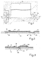
- This line comprises a plurality of turns and forms a helical winding. It can be obtained by winding the cable 1 on a cylindrical mandrel 2 with or without a magnetic core, depending on the sensitivity and the desired frequency response.
- the external conductor 3 of the coaxial is interrupted on a portion of the line so as to prevent the shield 3 from forming a short-circuited turn which would be the seat of eddy currents.
- the stripped portions are regularly located along the line at distances corresponding to the length of a turn, the winding forming a regular helix around a straight cylinder and the stripped portions being aligned parallel to the axis of the cylinder.
- the ends of the line are adapted and connected to an annex 4 alternating current measuring device for measuring the current induced by the magnetic field in the sensor winding.
- this adaptation can be carried out with discrete elements as shown, in general purely resistive elements of Zc value.
- Other adaptation means are provided for each stripped portion of shielding to compensate for the corresponding impedance break and preserve the adaptation of the line. This can be done with one or more impedances whose equivalent value is equal to the characteristic impedance Zc of the cable.
- each portion has two discrete elements of value 2Zc each, respectively connecting the central conductor 5 in this portion to the outer shield 3 at each end of the cable leading to this portion.
- the portions released by interruption of the shield 3, as well as the reported adaptation impedances can be shielded locally.
- Fig. 2 shows a corresponding embodiment at the location of a free area of external shielding 3, the adaptation resistors R1 and R2 have the value 2Zc and are arranged as well as the area in question inside a metal sleeve 6
- a metal plate or screen 7 constituting a low impedance conductor is used to connect each of the sleeves such as 6 to earth, that is to say to the external conductor 3.
- This connection cannot in fact be made to the stripped part because we would reproduce with the shielding 6 and the conductor 3 near a short-circuited turn; the connection is advantageously carried out with the diametrically opposite point because the most distant from the sleeve.
- the plate 6 is welded at A to the sleeve and opposite to the welding points 8 and C with the outer sheath 3 of the cable.
- Fig. 3 shows in section an alternative embodiment of the adaptation using coaxial elements integrated into the structure of the line in the form of two coaxial resistors R3 and R4 each of value 2Zc. These resistive elements are of known type, and used to constitute terminal load resistance for coaxial lines.
- the senor according to the invention can equally well be defined by a plurality of coaxial line elements connected end to end to connect their central conductor, each element having the shape of a turn and a length a little lower than that of a turn to provide each time a portion of stripped line of the shield 3.
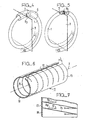
- Figs. 6 and 7 relate to embodiments with a strip line (called strip line in Anglo-Saxon) carried by a flexible or rigid insulating support.
- the coil may or may not contain a magnetic core depending on the desired sensitivity and frequency response.
- the external conductor of the line shielding
- the line is adapted by one or more impedances whose equivalent value is equal to the characteristic impedance of the line.
- impedances can be made either in discrete elements, or using a resistive paste.
- the exposed parts of the line, following the interruption of the shielding, as well as the reported impedances can also be the subject of a shielding to increase the rejection of the electric field.
- Fig. 6 represents a device produced from a wound flexible printed circuit 11.
- This double-sided circuit comprises, on one side the ground plane 13 corresponding to the shielding of the line and, on the other, a series of parallel tracks 15 forming with the ground plane the different segments of strip line (strip-line ).
- the adaptation resistors R11, R12, etc. are placed at the ends of the tracks, the connections with the ground plane being made with metallized holes, such as 12. After wiring these resistors, the circuit shown in flat part in Fig. 7 to obtain the arrangement of FIG. 6, that is to say a cylinder but by leaving a space L between the edges coming opposite. Holding means not shown are provided (end collars, mandrel, etc.). The continuity of the line is ensured by connecting the ends of the turns 15 to each other by ends of conductors 19 to form a continuous helix.
- the ground plane 13 which is outside, thus remains interrupted to avoid creating a short-circuited turn.
- the rejection of the electric field is improved by a screen located above the slot and connected to earth by an appropriate link.
- Fig. 8 represents a sensor device produced from a rigid cylindrical tube 28 made of dielectric material. This tube is initially metallized by a deposit on its outer surface as well as on its inner surface. The external metallic coating will constitute the shield 23 of the ribbon line. The interruption of this shielding to spare the different portions of width L is obtained by machining (milling, abrasion, chemical etching, etc.). The internal deposit forms the strip 25 after machining, like a helical milling which removes unnecessary metal parts.
- Fig. 9 in detail shows in a cross section the mounting of adaptation resistors. These elements located at each turn at the location of the slot corresponding to the poor shielding portions are connected to the helical strip 25 by a series of metallized holes 22 located at the location of the slot.
- the matching resistors can be either discrete resistors between the metallized holes and the shielding, or a deposit of resistive paste adjusted by sandblasting, laser, etc.
- a screen placed above the slot and connected to earth by a suitable link improves the rejection of the electric field.
Landscapes
- Physics & Mathematics (AREA)
- Condensed Matter Physics & Semiconductors (AREA)
- General Physics & Mathematics (AREA)
- Measuring Magnetic Variables (AREA)
- Measuring Instrument Details And Bridges, And Automatic Balancing Devices (AREA)
Applications Claiming Priority (2)
| Application Number | Priority Date | Filing Date | Title |
|---|---|---|---|
| FR8217296A FR2534692A1 (fr) | 1982-10-15 | 1982-10-15 | Dispositif capteur de champ magnetique alternatif a haute sensibilite et a large bande, et appareil de mesure l'utilisant |
| FR8217296 | 1982-10-15 |
Publications (2)
| Publication Number | Publication Date |
|---|---|
| EP0109867A1 EP0109867A1 (fr) | 1984-05-30 |
| EP0109867B1 true EP0109867B1 (fr) | 1986-04-09 |
Family
ID=9278312
Family Applications (1)
| Application Number | Title | Priority Date | Filing Date |
|---|---|---|---|
| EP83401944A Expired EP0109867B1 (fr) | 1982-10-15 | 1983-10-04 | Dispositif capteur de champ magnétique alternatif à haute sensibilité, et à large bande, et appareil de mesure l'utilisant |
Country Status (5)
| Country | Link |
|---|---|
| US (1) | US4605899A (OSRAM) |
| EP (1) | EP0109867B1 (OSRAM) |
| CA (1) | CA1205524A (OSRAM) |
| DE (1) | DE3362942D1 (OSRAM) |
| FR (1) | FR2534692A1 (OSRAM) |
Families Citing this family (22)
| Publication number | Priority date | Publication date | Assignee | Title |
|---|---|---|---|---|
| JPS61128609A (ja) * | 1984-11-27 | 1986-06-16 | Toyota Motor Corp | 自動車用アンテナ装置 |
| FR2583171B1 (fr) * | 1985-06-07 | 1988-06-17 | Commissariat Energie Atomique | Detecteur de champ magnetique a large bande passante en frequence |
| DE3675339D1 (de) * | 1985-11-18 | 1990-12-06 | Siemens Ag | Oberflaechenspule fuer die untersuchung mit hilfe der kernmagnetischen resonanz. |
| NL8600730A (nl) * | 1986-03-21 | 1987-10-16 | Philips Nv | Magnetisch resonantie apparaat met storingsvrije rf spoel. |
| GB8613789D0 (en) * | 1986-06-06 | 1986-07-09 | Bonar Bray Ltd | Magnetic field sensor coil |
| US4790030A (en) * | 1986-11-25 | 1988-12-06 | Rca Licensing Corporation | Tuner with insertable antenna coupler |
| US5248989A (en) * | 1988-02-04 | 1993-09-28 | Unisan Ltd. | Magnetic field concentrator |
| US5130654A (en) * | 1989-06-16 | 1992-07-14 | University Of Virginia Alumni Patents Foundation | Magnetolelastic amorphous metal ribbon gradiometer |
| US5239290A (en) * | 1992-03-25 | 1993-08-24 | Schonstedt Instrument Company | Magnetic cores for saturable core measuring devices and methods of manufacturing such cores |
| US6204661B1 (en) | 1998-09-30 | 2001-03-20 | Tech International Corp. | Detector for periodic magnetic field |
| US6847210B1 (en) | 1999-12-17 | 2005-01-25 | Fonar Corporation | MRI antenna |
| US6636040B1 (en) | 1999-12-17 | 2003-10-21 | Fonar Corporation | MRI antenna |
| US6727698B1 (en) | 1999-12-17 | 2004-04-27 | Fonar Corporation | MRI antennas including electrically connected inner and outer conductors, and MRI systems including such antennas |
| GB0104910D0 (en) * | 2001-02-28 | 2001-04-18 | Ibm | Devices to reduce electro-magnetic field radiation |
| KR20060021649A (ko) * | 2004-09-03 | 2006-03-08 | 엘지전자 주식회사 | 고밀도 미세 패턴의 단락 도선 위치 검출을 위한 자기 센서 |
| KR20070086217A (ko) * | 2004-12-14 | 2007-08-27 | 알렉스 액셀로드 | 자기 유도 디바이스 |
| EP2735056B1 (de) * | 2011-07-22 | 2015-09-09 | Max-Planck-Gesellschaft zur Förderung der Wissenschaften e.V. | Antenne und antennenanordnung für magnetresonanz-anwendungen |
| US9519037B2 (en) | 2011-11-10 | 2016-12-13 | Mayo Foundation For Medical Education And Research | Spatially coincident MRI receiver coils and method for manufacturing |
| US9678180B2 (en) * | 2014-05-06 | 2017-06-13 | Quality Electrodynamics, Llc | Coaxial cable magnetic resonance image (MRI) coil |
| US9933501B2 (en) | 2014-08-04 | 2018-04-03 | Quality Electrodynamics, Llc | Magnetic resonance imaging (MRI) coil with integrated decoupling |
| US11686792B2 (en) * | 2017-04-30 | 2023-06-27 | New York University | Receive coil arrangement and method for use thereof |
| US10739422B2 (en) | 2017-05-16 | 2020-08-11 | Quality Electrodynamics, Llc | Flexible coaxial magnetic resonance imaging (MRI) coil with integrated decoupling |
Family Cites Families (12)
| Publication number | Priority date | Publication date | Assignee | Title |
|---|---|---|---|---|
| US1490382A (en) * | 1920-07-30 | 1924-04-15 | Gen Electric | Direct-reading flux meter |
| US2349154A (en) * | 1941-08-13 | 1944-05-16 | Finch Telecommunications Inc | Coaxial cable loop antenna |
| US2419577A (en) * | 1945-03-12 | 1947-04-29 | Standard Telephones Cables Ltd | Antenna system |
| US2465381A (en) * | 1945-03-12 | 1949-03-29 | Standard Telephones Cables Ltd | Loop antenna system |
| US2681434A (en) * | 1951-03-07 | 1954-06-15 | Boonton Radio Corp | Frequency meter |
| NL6701915A (OSRAM) * | 1967-02-08 | 1968-08-09 | ||
| US3662255A (en) * | 1970-04-13 | 1972-05-09 | Charles L Garrett | Apparatus for locating concealed or buried metal bodies and a stable inductor usable in such detectors |
| JPS5226879B2 (OSRAM) * | 1972-09-19 | 1977-07-16 | ||
| US3973263A (en) * | 1973-04-20 | 1976-08-03 | The United States Of America As Represented By The Secretary Of The Navy | Sensitivity improvement of spaced-loop antenna by capacitive gap loading |
| AU4414579A (en) * | 1978-02-22 | 1979-08-30 | General Electric Company Limited, The | Carrier domain current transducer |
| JPS57192877A (en) * | 1981-05-23 | 1982-11-27 | Toyota Central Res & Dev Lab Inc | Measuring device for intensity of electromagnetic field |
| US4433336A (en) * | 1982-02-05 | 1984-02-21 | The United States Of America As Represented By The Secretary Of Commerce | Three-element antenna formed of orthogonal loops mounted on a monopole |
-
1982
- 1982-10-15 FR FR8217296A patent/FR2534692A1/fr active Granted
-
1983
- 1983-10-04 DE DE8383401944T patent/DE3362942D1/de not_active Expired
- 1983-10-04 EP EP83401944A patent/EP0109867B1/fr not_active Expired
- 1983-10-11 US US06/541,004 patent/US4605899A/en not_active Expired - Fee Related
- 1983-10-12 CA CA000438815A patent/CA1205524A/en not_active Expired
Non-Patent Citations (2)
| Title |
|---|
| IEEE TRANSACTIONS ON ELECTROMAGNETIC COMPATIBILITY, vol. EMC-16, no. 2, mai 1974, New York (US) P.H. DUNCAN: "Analysis of the Moebius loop magnetic field sensor", pages 83-89 * |
| IEEE TRANSACTIONS ON INSTRUMENTATION AND MEASUREMENT, vol. IM-29, no. 4, décembre 1980, New York (US) I. YOKOSHIMA et al.: "HF magnetic field standard", pages 451-454 * |
Also Published As
| Publication number | Publication date |
|---|---|
| FR2534692B1 (OSRAM) | 1984-12-14 |
| FR2534692A1 (fr) | 1984-04-20 |
| EP0109867A1 (fr) | 1984-05-30 |
| US4605899A (en) | 1986-08-12 |
| CA1205524A (en) | 1986-06-03 |
| DE3362942D1 (en) | 1986-05-15 |
Similar Documents
| Publication | Publication Date | Title |
|---|---|---|
| EP0109867B1 (fr) | Dispositif capteur de champ magnétique alternatif à haute sensibilité, et à large bande, et appareil de mesure l'utilisant | |
| EP0573350B1 (fr) | Bobine de Rogowski | |
| EP1596206B1 (fr) | Dispositif de mesure d'un courant électrique, capteur de courant, déclencheur électrique et dispositif de coupure comportant un tel dispositif de mesure | |
| EP0051018A1 (fr) | Procédé et dispositif de diagraphie électromagnétique dans les forages | |
| WO2016142439A1 (fr) | Capteur de courant pour mesurer un courant alternatif | |
| EP0445017A1 (fr) | Résonateur coaxial à capacité d'accord répartie | |
| EP0363381B1 (fr) | Antenne electromagnetique et antenne d'excitation pour un appareil de resonance magnetique nucleaire munie d'une telle antenne electromagnetique | |
| FR2643749A1 (fr) | Dispositif de couplage d'une ligne coaxiale a haute frequence | |
| EP0239426B1 (fr) | Antenne de réception pour appareil d'imagerie par résonance magnétique nucléaire | |
| FR2665025A1 (fr) | Element de transition entre guides d'ondes electromagnetiques, notamment entre un guide d'ondes circulaire et un guide d'ondes coaxial. | |
| EP1607761B1 (fr) | Circuit d'alimention multifréquencielle et sonde et spectromètre RMN comportant un tel circuit | |
| EP0076193B1 (fr) | Procédé pour déterminer le seuil de résistance d'un équipement électrique ou électronique à une agression électromagnétique extérieure et dispositifs pour sa mise en oeuvre | |
| EP0102091A2 (fr) | Dispositif de diagraphie électromagnétique | |
| EP3443365B1 (fr) | Appareil de mesure de courants électriques | |
| EP0206879B1 (fr) | Détecteur de champ magnétique à large bande passante en fréquence | |
| EP4088381B1 (fr) | Dispositif de detection capacitive comprenant un module de polarisation par induction | |
| EP2753942B1 (fr) | Dispositif de mesure comportant un shunt et un compteur électrique comportant un tel dispositif de mesure | |
| EP0027067B1 (fr) | Antenne plane bifilaire à rayonnement transversal et son application aux aériens radars | |
| FR2670296A1 (fr) | Dispositif de mesure de l'impedance de transfert d'un cable. | |
| FR2871892A1 (fr) | Circuit d'alimentation d'une bobine et sonde et spectrometre rmn comportant un tel circuit | |
| FR2799840A1 (fr) | Capteur de courant differentiel | |
| WO2010119207A1 (fr) | Antenne radioélectrique, procédé de dimensionnement d'un corps plat de l'antenne, et procédé de fabrication d'une telle antenne | |
| WO1994028429A1 (fr) | Procede et dispositif pour la mesure de composantes dynamiques d'un courant electrique en presence d'une composante continue | |
| FR3155066A1 (fr) | Capteur de courant Rogowski comportant un circuit imprimé | |
| FR3057111A1 (fr) | Dispositif electronique a antenne isolee |
Legal Events
| Date | Code | Title | Description |
|---|---|---|---|
| PUAI | Public reference made under article 153(3) epc to a published international application that has entered the european phase |
Free format text: ORIGINAL CODE: 0009012 |
|
| AK | Designated contracting states |
Designated state(s): BE CH DE GB IT LI NL SE |
|
| 17P | Request for examination filed |
Effective date: 19841015 |
|
| RBV | Designated contracting states (corrected) |
Designated state(s): BE CH DE GB IT LI SE |
|
| GRAA | (expected) grant |
Free format text: ORIGINAL CODE: 0009210 |
|
| AK | Designated contracting states |
Kind code of ref document: B1 Designated state(s): BE CH DE GB IT LI SE |
|
| ITF | It: translation for a ep patent filed | ||
| REF | Corresponds to: |
Ref document number: 3362942 Country of ref document: DE Date of ref document: 19860515 |
|
| PLBE | No opposition filed within time limit |
Free format text: ORIGINAL CODE: 0009261 |
|
| STAA | Information on the status of an ep patent application or granted ep patent |
Free format text: STATUS: NO OPPOSITION FILED WITHIN TIME LIMIT |
|
| 26N | No opposition filed | ||
| ITTA | It: last paid annual fee | ||
| PGFP | Annual fee paid to national office [announced via postgrant information from national office to epo] |
Ref country code: SE Payment date: 19940919 Year of fee payment: 12 |
|
| PGFP | Annual fee paid to national office [announced via postgrant information from national office to epo] |
Ref country code: BE Payment date: 19940922 Year of fee payment: 12 |
|
| EAL | Se: european patent in force in sweden |
Ref document number: 83401944.0 |
|
| PG25 | Lapsed in a contracting state [announced via postgrant information from national office to epo] |
Ref country code: SE Effective date: 19951005 |
|
| PG25 | Lapsed in a contracting state [announced via postgrant information from national office to epo] |
Ref country code: BE Effective date: 19951031 |
|
| BERE | Be: lapsed |
Owner name: THOMSON-CSF Effective date: 19951031 |
|
| EUG | Se: european patent has lapsed |
Ref document number: 83401944.0 |
|
| PGFP | Annual fee paid to national office [announced via postgrant information from national office to epo] |
Ref country code: CH Payment date: 19970916 Year of fee payment: 15 |
|
| PGFP | Annual fee paid to national office [announced via postgrant information from national office to epo] |
Ref country code: GB Payment date: 19970918 Year of fee payment: 15 Ref country code: DE Payment date: 19970918 Year of fee payment: 15 |
|
| PG25 | Lapsed in a contracting state [announced via postgrant information from national office to epo] |
Ref country code: GB Free format text: LAPSE BECAUSE OF NON-PAYMENT OF DUE FEES Effective date: 19981004 |
|
| PG25 | Lapsed in a contracting state [announced via postgrant information from national office to epo] |
Ref country code: LI Free format text: LAPSE BECAUSE OF NON-PAYMENT OF DUE FEES Effective date: 19981031 Ref country code: CH Free format text: LAPSE BECAUSE OF NON-PAYMENT OF DUE FEES Effective date: 19981031 |
|
| GBPC | Gb: european patent ceased through non-payment of renewal fee |
Effective date: 19981004 |
|
| REG | Reference to a national code |
Ref country code: CH Ref legal event code: PL |
|
| PG25 | Lapsed in a contracting state [announced via postgrant information from national office to epo] |
Ref country code: DE Free format text: LAPSE BECAUSE OF NON-PAYMENT OF DUE FEES Effective date: 19990803 |