EP0109137A2 - Partial product accumulation in high performance multipliers - Google Patents
Partial product accumulation in high performance multipliers Download PDFInfo
- Publication number
- EP0109137A2 EP0109137A2 EP83303303A EP83303303A EP0109137A2 EP 0109137 A2 EP0109137 A2 EP 0109137A2 EP 83303303 A EP83303303 A EP 83303303A EP 83303303 A EP83303303 A EP 83303303A EP 0109137 A2 EP0109137 A2 EP 0109137A2
- Authority
- EP
- European Patent Office
- Prior art keywords
- operand
- cell
- producing
- bit
- partial product
- Prior art date
- Legal status (The legal status is an assumption and is not a legal conclusion. Google has not performed a legal analysis and makes no representation as to the accuracy of the status listed.)
- Granted
Links
Images


Classifications
-
- G—PHYSICS
- G06—COMPUTING; CALCULATING OR COUNTING
- G06F—ELECTRIC DIGITAL DATA PROCESSING
- G06F7/00—Methods or arrangements for processing data by operating upon the order or content of the data handled
- G06F7/38—Methods or arrangements for performing computations using exclusively denominational number representation, e.g. using binary, ternary, decimal representation
- G06F7/48—Methods or arrangements for performing computations using exclusively denominational number representation, e.g. using binary, ternary, decimal representation using non-contact-making devices, e.g. tube, solid state device; using unspecified devices
- G06F7/52—Multiplying; Dividing
- G06F7/523—Multiplying only
- G06F7/533—Reduction of the number of iteration steps or stages, e.g. using the Booth algorithm, log-sum, odd-even
-
- G—PHYSICS
- G06—COMPUTING; CALCULATING OR COUNTING
- G06F—ELECTRIC DIGITAL DATA PROCESSING
- G06F7/00—Methods or arrangements for processing data by operating upon the order or content of the data handled
- G06F7/38—Methods or arrangements for performing computations using exclusively denominational number representation, e.g. using binary, ternary, decimal representation
- G06F7/48—Methods or arrangements for performing computations using exclusively denominational number representation, e.g. using binary, ternary, decimal representation using non-contact-making devices, e.g. tube, solid state device; using unspecified devices
- G06F7/50—Adding; Subtracting
- G06F7/505—Adding; Subtracting in bit-parallel fashion, i.e. having a different digit-handling circuit for each denomination
- G06F7/509—Adding; Subtracting in bit-parallel fashion, i.e. having a different digit-handling circuit for each denomination for multiple operands, e.g. digital integrators
Definitions
- the present invention is concerned with partial product accumulation in high performance multipliers.
- the multiplication of two N-bit operands is a fundamental operation in general purpose computer processors.
- the first operand A is successively multiplied by each bit of the second operand B to create a partial product.
- the partial product is then shifted to assign the appropriate weight based on the weight of the corresponding digit of the second operand B.
- the shifted partial products are added together, i.e., accumulated, to form the final product D.
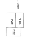
- Figure 1 A complete 8x8 encoded binary multiplier is shown in Figure 1 of the accompanying drawings with the related Boolean equations in Table 1.
- Figure 1 consists of four sections: encoder logic 10, ripple accumulator 20, negative B operand correction 30, and a carry propagate adder 40.
- the operands are A (0-7) and B (0-7) and the product is D(0-15).
- HADD and FADD are conventional half adders and full adders respectively with carry (C) and sum (S) outputs.
- the symbols XP2, XP1, XO, XM1, and XM2 are used for the X(+2), X(+l), X (0), X (-1), and X (-2) encoded digits for clarity.
- "*" is the Boolean "AND”
- "+” is the Boolean "OR”
- XOR is the Boolean "Exclusive-OR”.
- the logic block Ll consists of logic to select X(+2), X (+1), X (0); X (-1) or X (-2) multiples of the A operand.
- the multiples of B are generated in the array by simple shifting, complementing, or masking operations.
- the block L2 generates the lost bit that results from the single shift used to generate an X(+2) or X(-2) multiple.
- the logic block L3 incorporates the signed digit encoding set of Table 2 as proposed by Booth.
- the block L3 also performs an effective sign extension of each partial product to 16 bits.
- the signal Minus(J) indicates that at least one previous bit pair generated a negative partial product. This signal is combined with the signed digit multiplier of a bit pair to generate bit (2J) and bit (2J+1). These two signals are the effective sign extension for each partial product fully merged with the sign extensions of all previously generated partial products.
- the logic blocks L4 and L5 perform a correction for a negative B operand and for a signed digit carry out of the last multiplier bit pair.
- the blocks L6 and L7 perform a two's complement operation on the A operand for X(-l) and X(-2) signed digits.
- this ripple adder technique is that it is usually convenient to lay out the required circuitry in monolithic single chip form.
- this technique is generally quite slow because the partial product accumulation takes place in ripple fashion, and the worst case delay path must pass through all of the rows of full adders.
- the worst case delay will be equivalent to four full adder delays. Without encoding, the worst case delay would be eight full adder delays. In the case of a 64x64 multiplier with encoding, the worst case delay would be thirty-two, and without encoding the maximum delay would be sixty-four full adder delays.
- the present invention provides a circuit for accumulating partial products in a multiplier of first and second N-bit operands, said accumulator circuit being characterized in that a plurality of block means having rows of cells arrayed as a matrix is provided for producing a set of local and global ripple signals.
- the present invention provides a circuit for accumulating partial products in a multiplier of first and second N-bit operands, said accumulator circuit being characterized by a plurality of block means arrayed as a matrix having a first cell means coupled to a digit of both said first operand and second operand for producing a first set of local ripple signals; a plurality of second cell means coupled to a digit of both said first operand and said second operand for producing a second set of local ripple signals; a plurality of third cell means coupled to a digit of both said first operand and second operand for producing a third set of local ripple signals; a plurality of fourth cell means coupled to a digit of both said first operand and said second operand for producing a fourth set of local ripple signals; a plurality of fifth cell means coupled to said second operand for producing a first set of partial product signals; a plurality of sixth cell means coupled to said second operand for producing a second set of partial product signals; a plurality of seventh cell means coupled to said second
- the cells are preferably one bit by one bit in area and the length of the matrix of the block means may form an arithmetic progression.
- the present invention replaces the standard ripple accumulator 20 described in Figure 1.
- This new technique requires fewer than 5% more transistors to implement than the prior art shown in Figure 1 yet is able to provide more than three times the performance of the prior technique for a 64x64 multiplier.
- the present invention can perform a 64x64 multiply with only 10 full adder delays. This compares favorably with the theoretical minimum delay of 8 full adders as explained by C.S. Wallace in "A Suggestion for a Fast Multiplier", IEEE Transactions on Electronic Computers, pp. 14-17 (Feb. 1964).
- the new technique involves breaking the rows of the accumulator array into blocks.
- the blocks themselves are of varying length and are implemented as a series of one-bit ripple cells.
- To implement a multiplier of any desired precision only eight different cell types are required for the entire accumulator.
- the accumulation of the blocks still occurs in ripple fashion, but the ripple of the blocks occurs in parallel.
- the number of cells per block is arranged as an arithmetic progression to match the desired precision of the multiplication with the result that after the local ripple of the first block, each additional block requires only two more full adder delays.
- the present technique can be used to provide for the accumulation of partial product terms in a high precision, high performance multiplier.
- the method is easily expandable to any desired precision. It is especially suited for utilization in a monolithic VLSI multiplier because of its high speed, low complexity, and straightforward mask design.
- the present technique will be implemented in a multiplier which employs some form of encoding, as described earlier, since encoding can reduce the size of the accumulator by one-half, while the encoding itself usually requires only simple logic gates or multiplexors.
- the disclosed technique is a general method of accumulation and will function in a system which does not utilize encoding at all.
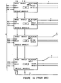
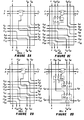
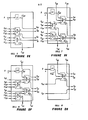
- FIGS 2A-2H show the complete set of cells necessary to implement the present digital accumulator. Shown are cells 1-8, respectively, which are organized, for example, as shown in Figure 3 to form a 64x64 bit memory array which can replace the ripple accumulator array 20 of the type shown in Figure 1. Cells 1-4 are used in the main array 310 of Figure 3. Each cell is one bit by one bit in area, thus requiring a main array 310 of 64x32 cells in the example shown in Figure 3 where encoding is assumed.
- the logic elements surrounding the main array 310 are unchanged except for a single column 320 of end cells 5-8 which are also one bit in area as shown in Figures 2E-2H respectively, on the right side of the array 310.
- the logic element Ll used in the cells 1-4 and the logic element L6 used in the cells 5-8 are the same elements as are used in the prior art as illustrated in Table 1.
- the full adders FADD are also of convention design as used in the prior art.
- the accumulation technique involves breaking the rows of the matrix array 310 with the end column 320 into blocks.
- the 32 rows of partial product blocks are broken into five blocks 1-5 of height 4, 4, 6, 8, and 10 bit rows.
- Each row is coupled to one pair of encoded B operand bits.
- the matrix array 310 is composed of 64 columns of cells as shown by a bit slice 330. Each slice 330 is coupled to one bit of the A operand.
- Each slice 330 of blocks 1-5 in the main array 310 is implemented as a cell 1, followed by a cell 2, followed by one or more of continue cells 3, and finished by a cell 4.
- the end cell slice 320 of each block 1-5 is implemented as a cell 5, followed by a cell 6, followed by one or more of cells 7, and finished by a cell 8.
- Each block 1-5 performs a local ripple accumulation of its partial product terms, labeled as LC a, and LCb , with a relative weight depending on.the corresponding row position of the cell involved.
- LCa5 is a local ripple term with a relative bit weight of 5.
- the ripple accumulation of the blocks 1-5 is accomplished by the global ripple terms Ga and G b , and occurs in parallel.
- the length of the blocks 1-5 is selected to form an arithmetic progression, for example, 4-4-6-8-10 as illustrated in Figure 3, which matches the number of partial products required.
- An ideal progression would be of the form 1-2-3-4-5, but the sum of the lengths must match the number of partial products and the technique requires four rows in the first block as explained above.
- a progression of 4-6-6 would best match an accumulator with sixteen partial products and 4-4-6-8-10 effectively matches a system with 32 partial products.
- the cell 4 of block 1 may be modified as shown in Figure 4 to remove the logically redundant full adders in that cell to attain the minimum overall delay in the entire array 310.
Abstract
Description
- The present invention is concerned with partial product accumulation in high performance multipliers.
- The multiplication of two N-bit operands is a fundamental operation in general purpose computer processors. To perform a longhand multiplication the first operand A is successively multiplied by each bit of the second operand B to create a partial product. The partial product is then shifted to assign the appropriate weight based on the weight of the corresponding digit of the second operand B. Finally, the shifted partial products are added together, i.e., accumulated, to form the final product D.
- Several techniques have been devised to speed up and/or simplify the longhand multiplication described above. Usually, as explained by A. Booth, in "A Signed Binary Multiplication Technique", Quarterly Journal of Mechanics and Applied Mathematics, Vol. IV, pt. 2, pp. 236-240 (1951), an encoding scheme is performed on the bits of the B operand by means of a signed-digit-carry set (SDC) of, for example, +2, +1, 0, -1, and -2, to reduce the number of partial products to be accumulated by one-half. The accumulation is then performed in a ripple fashion through the use of full adders arranged in a carry save format. Each partial product bit still requires one full adder.
- A complete 8x8 encoded binary multiplier is shown in Figure 1 of the accompanying drawings with the related Boolean equations in Table 1. Figure 1 consists of four sections:
encoder logic 10,ripple accumulator 20, negativeB operand correction 30, and a carry propagate adder 40.
- The inputs TCA and TCB indicate whether the A and B operands are two's complement (=1) or unsigned (=0). The symbols XP2, XP1, XO, XM1, and XM2 are used for the X(+2), X(+l), X (0), X (-1), and X (-2) encoded digits for clarity. "*" is the Boolean "AND", "+" is the Boolean "OR", and "XOR" is the Boolean "Exclusive-OR".
- In Table 1, the logic block Ll consists of logic to select X(+2), X (+1), X (0); X (-1) or X (-2) multiples of the A operand. The multiples of B are generated in the array by simple shifting, complementing, or masking operations. The block L2 generates the lost bit that results from the single shift used to generate an X(+2) or X(-2) multiple.

- The logic block L3 incorporates the signed digit encoding set of Table 2 as proposed by Booth. The block L3 also performs an effective sign extension of each partial product to 16 bits. The signal Minus(J) indicates that at least one previous bit pair generated a negative partial product. This signal is combined with the signed digit multiplier of a bit pair to generate bit (2J) and bit (2J+1). These two signals are the effective sign extension for each partial product fully merged with the sign extensions of all previously generated partial products. The logic blocks L4 and L5 perform a correction for a negative B operand and for a signed digit carry out of the last multiplier bit pair. The blocks L6 and L7 perform a two's complement operation on the A operand for X(-l) and X(-2) signed digits.
- The advantage of this ripple adder technique is that it is usually convenient to lay out the required circuitry in monolithic single chip form. However, this technique is generally quite slow because the partial product accumulation takes place in ripple fashion, and the worst case delay path must pass through all of the rows of full adders. For example, in the case of the 8x8 multiplier with encoding as shown in Figure 1 which will have four 8-bit partial products, the worst case delay will be equivalent to four full adder delays. Without encoding, the worst case delay would be eight full adder delays. In the case of a 64x64 multiplier with encoding, the worst case delay would be thirty-two, and without encoding the maximum delay would be sixty-four full adder delays.
- The present invention provides a circuit for accumulating partial products in a multiplier of first and second N-bit operands, said accumulator circuit being characterized in that a plurality of block means having rows of cells arrayed as a matrix is provided for producing a set of local and global ripple signals.
- The present invention provides a circuit for accumulating partial products in a multiplier of first and second N-bit operands, said accumulator circuit being characterized by a plurality of block means arrayed as a matrix having a first cell means coupled to a digit of both said first operand and second operand for producing a first set of local ripple signals; a plurality of second cell means coupled to a digit of both said first operand and said second operand for producing a second set of local ripple signals; a plurality of third cell means coupled to a digit of both said first operand and second operand for producing a third set of local ripple signals; a plurality of fourth cell means coupled to a digit of both said first operand and said second operand for producing a fourth set of local ripple signals; a plurality of fifth cell means coupled to said second operand for producing a first set of partial product signals; a plurality of sixth cell means coupled to said second operand for producing a second set of partial product signals; a plurality of seventh cell means coupled to said second operand for producing a third set of partial product signals; and a plurality of eighth cell means coupled to said second operand for producing a fourth set of partial product signals for producing a set of global ripple signals connected as an array with a first row of said first and fifth cell means, a second row of said second and sixth cell means, a plurality of third rows of said third and seventh cell means, and a fourth row of said fourth and eighth cell means.
- The cells are preferably one bit by one bit in area and the length of the matrix of the block means may form an arithmetic progression.
- The present invention replaces the
standard ripple accumulator 20 described in Figure 1. This new technique requires fewer than 5% more transistors to implement than the prior art shown in Figure 1 yet is able to provide more than three times the performance of the prior technique for a 64x64 multiplier. Thus, rather than 32 full adder delays, the present invention can perform a 64x64 multiply with only 10 full adder delays. This compares favorably with the theoretical minimum delay of 8 full adders as explained by C.S. Wallace in "A Suggestion for a Fast Multiplier", IEEE Transactions on Electronic Computers, pp. 14-17 (Feb. 1964). - The new technique involves breaking the rows of the accumulator array into blocks. The blocks themselves are of varying length and are implemented as a series of one-bit ripple cells. To implement a multiplier of any desired precision only eight different cell types are required for the entire accumulator. The accumulation of the blocks still occurs in ripple fashion, but the ripple of the blocks occurs in parallel. The number of cells per block is arranged as an arithmetic progression to match the desired precision of the multiplication with the result that after the local ripple of the first block, each additional block requires only two more full adder delays.
- Thus, the present technique can be used to provide for the accumulation of partial product terms in a high precision, high performance multiplier. The method is easily expandable to any desired precision. It is especially suited for utilization in a monolithic VLSI multiplier because of its high speed, low complexity, and straightforward mask design.
- Generally, the present technique will be implemented in a multiplier which employs some form of encoding, as described earlier, since encoding can reduce the size of the accumulator by one-half, while the encoding itself usually requires only simple logic gates or multiplexors. However, the disclosed technique is a general method of accumulation and will function in a system which does not utilize encoding at all.
- There now follows a detailed description which is to be read with reference to Figures 2 to 4 of the accompanying drawings of a circuit according to the present invention; it is to be clearly understood that the circuit has been selected for description to illustrate the invention by way of example and not by way of limitation.
- In the accompanying drawings:
- Figures 2A-2H show the set of cells required to implement the accumulation circuit of the present invention;
- Figure 3 shows the organization of the cells of Figures 2A-2H into blocks to form a 64x64 bit accumulator with encoded B inputs; and
- Figure 4 shows a modified version of the cell of Figure 2D to attain the minimum circuit delay.
- Figures 2A-2H show the complete set of cells necessary to implement the present digital accumulator. Shown are cells 1-8, respectively, which are organized, for example, as shown in Figure 3 to form a 64x64 bit memory array which can replace the
ripple accumulator array 20 of the type shown in Figure 1. Cells 1-4 are used in themain array 310 of Figure 3. Each cell is one bit by one bit in area, thus requiring amain array 310 of 64x32 cells in the example shown in Figure 3 where encoding is assumed. The logic elements surrounding the main array 310 (encoder logic 10,negative operand correction 30, and the carry propagate adder 40 shown in Figure 1) are unchanged except for asingle column 320 of end cells 5-8 which are also one bit in area as shown in Figures 2E-2H respectively, on the right side of thearray 310. The logic element Ll used in the cells 1-4 and the logic element L6 used in the cells 5-8 are the same elements as are used in the prior art as illustrated in Table 1. The full adders FADD are also of convention design as used in the prior art. - As shown in Figure 3, the accumulation technique involves breaking the rows of the
matrix array 310 with theend column 320 into blocks. In the 64 bit example shown, the 32 rows of partial product blocks are broken into five blocks 1-5 ofheight matrix array 310 is composed of 64 columns of cells as shown by abit slice 330. Eachslice 330 is coupled to one bit of the A operand. - Each
slice 330 of blocks 1-5 in themain array 310 is implemented as acell 1, followed by acell 2, followed by one or more ofcontinue cells 3, and finished by acell 4. Similarly, theend cell slice 320 of each block 1-5 is implemented as acell 5, followed by acell 6, followed by one or more ofcells 7, and finished by acell 8. Each block 1-5 performs a local ripple accumulation of its partial product terms, labeled as LCa, and LCb, with a relative weight depending on.the corresponding row position of the cell involved. For example, LCa5 is a local ripple term with a relative bit weight of 5. - The ripple accumulation of the blocks 1-5 is accomplished by the global ripple terms Ga and Gb, and occurs in parallel. The length of the blocks 1-5 is selected to form an arithmetic progression, for example, 4-4-6-8-10 as illustrated in Figure 3, which matches the number of partial products required. An ideal progression would be of the form 1-2-3-4-5, but the sum of the lengths must match the number of partial products and the technique requires four rows in the first block as explained above. Thus, a progression of 4-6-6 would best match an accumulator with sixteen partial products and 4-4-6-8-10 effectively matches a system with 32 partial products. The result of arranging the length of blocks to form an arithmetic progression is that as
block 1 finishes rippling, its terms are ready to be accumulated into the two global bits Ga and Gb along with the output terms ofblock 2. The output terms ofblock 2 then pass down thearray 310 and end theslice 320 and are accumulated with the local bits LCa and LCb ofblock 3, and so on. The result is that afterblock 1, each additional block requires only two more full adder delays. - As each local bit LCa or LCb or global bit Ga and Gb is passed down the
array 310 with 320 from one row to the next, it must be shifted two bits to the right in order to be assigned the proper bit weight. This is the reason for the additional full adders in the cells 5-g in theend slice 320. The result is that the total number of intermediate product terms Pa and Pb is reduced to two terms per bit so that the imtermediate product terms Pa and Pb may then pass on to a conventional carry propagate adder 40 (Figure 1), which adder 40 produces the final multiplier product bits D. - Since the first global bits Ga and Gb on the top row of the
main array 310 are all zero, as shown in Figure 1, thecell 4 ofblock 1 may be modified as shown in Figure 4 to remove the logically redundant full adders in that cell to attain the minimum overall delay in theentire array 310.
Claims (4)
Applications Claiming Priority (2)
| Application Number | Priority Date | Filing Date | Title |
|---|---|---|---|
| US06/434,298 US4545028A (en) | 1982-10-13 | 1982-10-13 | Partial product accumulation in high performance multipliers |
| US434298 | 1982-10-13 |
Publications (3)
| Publication Number | Publication Date |
|---|---|
| EP0109137A2 true EP0109137A2 (en) | 1984-05-23 |
| EP0109137A3 EP0109137A3 (en) | 1986-05-14 |
| EP0109137B1 EP0109137B1 (en) | 1990-10-10 |
Family
ID=23723657
Family Applications (1)
| Application Number | Title | Priority Date | Filing Date |
|---|---|---|---|
| EP83303303A Expired EP0109137B1 (en) | 1982-10-13 | 1983-06-08 | Partial product accumulation in high performance multipliers |
Country Status (4)
| Country | Link |
|---|---|
| US (1) | US4545028A (en) |
| EP (1) | EP0109137B1 (en) |
| JP (1) | JPS5981737A (en) |
| DE (1) | DE3381935D1 (en) |
Cited By (2)
| Publication number | Priority date | Publication date | Assignee | Title |
|---|---|---|---|---|
| WO1990000773A1 (en) * | 1988-07-13 | 1990-01-25 | Siemens Aktiengesellschaft | Multiplier |
| KR101125391B1 (en) * | 2004-07-29 | 2012-04-02 | 에꼴 뽈리떼끄닉 뻬데랄 드 로잔느 (으뻬에프엘) | 2,2-bipyridine ligand, sensitizing dye and dye sensitized solar cell |
Families Citing this family (8)
| Publication number | Priority date | Publication date | Assignee | Title |
|---|---|---|---|---|
| US4577282A (en) | 1982-02-22 | 1986-03-18 | Texas Instruments Incorporated | Microcomputer system for digital signal processing |
| US4646257A (en) * | 1983-10-03 | 1987-02-24 | Texas Instruments Incorporated | Digital multiplication circuit for use in a microprocessor |
| US4680701A (en) * | 1984-04-11 | 1987-07-14 | Texas Instruments Incorporated | Asynchronous high speed processor having high speed memories with domino circuits contained therein |
| JPS61114338A (en) * | 1984-11-09 | 1986-06-02 | Hitachi Ltd | Multiplier |
| US4831577A (en) * | 1986-09-17 | 1989-05-16 | Intersil, Inc. | Digital multiplier architecture with triple array summation of partial products |
| US4839848A (en) * | 1987-09-14 | 1989-06-13 | Unisys Corporation | Fast multiplier circuit incorporating parallel arrays of two-bit and three-bit adders |
| DE69130652T2 (en) * | 1990-03-20 | 1999-05-06 | Fujitsu Ltd | Digital high speed parallel multiplier |
| US5808927A (en) * | 1994-10-18 | 1998-09-15 | International Business Machines Corporation | Apparatus for performing two's complement and unsigned multiply accumulate |
Citations (1)
| Publication number | Priority date | Publication date | Assignee | Title |
|---|---|---|---|---|
| US3700875A (en) * | 1970-02-18 | 1972-10-24 | Licentia Gmbh | Parallel binary carry look-ahead adder system |
Family Cites Families (2)
| Publication number | Priority date | Publication date | Assignee | Title |
|---|---|---|---|---|
| JPS5270727A (en) * | 1975-12-10 | 1977-06-13 | Fujitsu Ltd | Computation system |
| US4153938A (en) * | 1977-08-18 | 1979-05-08 | Monolithic Memories Inc. | High speed combinatorial digital multiplier |
-
1982
- 1982-10-13 US US06/434,298 patent/US4545028A/en not_active Expired - Lifetime
-
1983
- 1983-06-08 DE DE8383303303T patent/DE3381935D1/en not_active Expired - Lifetime
- 1983-06-08 EP EP83303303A patent/EP0109137B1/en not_active Expired
- 1983-09-27 JP JP58179051A patent/JPS5981737A/en active Granted
Patent Citations (1)
| Publication number | Priority date | Publication date | Assignee | Title |
|---|---|---|---|---|
| US3700875A (en) * | 1970-02-18 | 1972-10-24 | Licentia Gmbh | Parallel binary carry look-ahead adder system |
Non-Patent Citations (1)
| Title |
|---|
| ELECTRONICS LETTERS, vol. 7, no. 25, 16th December 1971, pages 747-749, Hitchin, Herts, GB; C.R. EDWARDS: "Floating-point cellular-logic multiplier with variable dynamic range" * |
Cited By (2)
| Publication number | Priority date | Publication date | Assignee | Title |
|---|---|---|---|---|
| WO1990000773A1 (en) * | 1988-07-13 | 1990-01-25 | Siemens Aktiengesellschaft | Multiplier |
| KR101125391B1 (en) * | 2004-07-29 | 2012-04-02 | 에꼴 뽈리떼끄닉 뻬데랄 드 로잔느 (으뻬에프엘) | 2,2-bipyridine ligand, sensitizing dye and dye sensitized solar cell |
Also Published As
| Publication number | Publication date |
|---|---|
| EP0109137A3 (en) | 1986-05-14 |
| US4545028A (en) | 1985-10-01 |
| JPS5981737A (en) | 1984-05-11 |
| EP0109137B1 (en) | 1990-10-10 |
| JPH0312738B2 (en) | 1991-02-20 |
| DE3381935D1 (en) | 1990-11-15 |
Similar Documents
| Publication | Publication Date | Title |
|---|---|---|
| EP0260515B1 (en) | Digital multiplier architecture with triple array summation of partial products | |
| US5787029A (en) | Ultra low power multiplier | |
| JP3244506B2 (en) | Small multiplier | |
| Taylor | Radix 16 SRT dividers with overlapped quotient selection stages: A 225 nanosecond double precision divider for the S-1 Mark IIB | |
| US5465226A (en) | High speed digital parallel multiplier | |
| EP0018519B1 (en) | Multiplier apparatus having a carry-save/propagate adder | |
| US4489393A (en) | Monolithic discrete-time digital convolution circuit | |
| US3670956A (en) | Digital binary multiplier employing sum of cross products technique | |
| US5161119A (en) | Weighted-delay column adder and method of organizing same | |
| US4965762A (en) | Mixed size radix recoded multiplier | |
| EP0098685B1 (en) | Multiple bit encoding technique for combinational multipliers | |
| US6018758A (en) | Squarer with diagonal row merged into folded partial product array | |
| EP0109137A2 (en) | Partial product accumulation in high performance multipliers | |
| JPH07191832A (en) | Binary-number squaring circuit | |
| US5944776A (en) | Fast carry-sum form booth encoder | |
| EP0398568A2 (en) | Multiplier circuit | |
| US6535901B1 (en) | Method and apparatus for generating a fast multiply accumulator | |
| US5497343A (en) | Reducing the number of carry-look-ahead adder stages in high-speed arithmetic units, structure and method | |
| EP0670061B1 (en) | Enhanced fast multiplier | |
| WO1991000568A1 (en) | Conditional-sum carry structure compiler | |
| EP0112186B1 (en) | Modular high-speed multipliers, and integrated circuit chip modules for such multipliers | |
| US4523210A (en) | Fast error checked multibit multiplier | |
| US5883825A (en) | Reduction of partial product arrays using pre-propagate set-up | |
| EP0318223A3 (en) | High speed parallel multiplier circuit | |
| JPH05173761A (en) | Binary integer multiplier |
Legal Events
| Date | Code | Title | Description |
|---|---|---|---|
| PUAI | Public reference made under article 153(3) epc to a published international application that has entered the european phase |
Free format text: ORIGINAL CODE: 0009012 |
|
| 17P | Request for examination filed |
Effective date: 19830613 |
|
| AK | Designated contracting states |
Designated state(s): DE FR GB |
|
| PUAL | Search report despatched |
Free format text: ORIGINAL CODE: 0009013 |
|
| AK | Designated contracting states |
Kind code of ref document: A3 Designated state(s): DE FR GB |
|
| 17Q | First examination report despatched |
Effective date: 19871125 |
|
| GRAA | (expected) grant |
Free format text: ORIGINAL CODE: 0009210 |
|
| AK | Designated contracting states |
Kind code of ref document: B1 Designated state(s): DE FR GB |
|
| REF | Corresponds to: |
Ref document number: 3381935 Country of ref document: DE Date of ref document: 19901115 |
|
| ET | Fr: translation filed | ||
| PLBE | No opposition filed within time limit |
Free format text: ORIGINAL CODE: 0009261 |
|
| STAA | Information on the status of an ep patent application or granted ep patent |
Free format text: STATUS: NO OPPOSITION FILED WITHIN TIME LIMIT |
|
| 26N | No opposition filed | ||
| PGFP | Annual fee paid to national office [announced via postgrant information from national office to epo] |
Ref country code: DE Payment date: 19960528 Year of fee payment: 14 |
|
| PG25 | Lapsed in a contracting state [announced via postgrant information from national office to epo] |
Ref country code: DE Free format text: LAPSE BECAUSE OF NON-PAYMENT OF DUE FEES Effective date: 19980303 |
|
| REG | Reference to a national code |
Ref country code: GB Ref legal event code: 732E |
|
| REG | Reference to a national code |
Ref country code: GB Ref legal event code: IF02 |
|
| PGFP | Annual fee paid to national office [announced via postgrant information from national office to epo] |
Ref country code: FR Payment date: 20020517 Year of fee payment: 20 |
|
| REG | Reference to a national code |
Ref country code: FR Ref legal event code: TP |
|
| PGFP | Annual fee paid to national office [announced via postgrant information from national office to epo] |
Ref country code: GB Payment date: 20020605 Year of fee payment: 20 |
|
| PG25 | Lapsed in a contracting state [announced via postgrant information from national office to epo] |
Ref country code: GB Free format text: LAPSE BECAUSE OF EXPIRATION OF PROTECTION Effective date: 20030607 |
|
| REG | Reference to a national code |
Ref country code: GB Ref legal event code: PE20 |