EP0108670B1 - Dispositif d'alimentation d'une antenne réseau à faisceau de balayage - Google Patents
Dispositif d'alimentation d'une antenne réseau à faisceau de balayage Download PDFInfo
- Publication number
- EP0108670B1 EP0108670B1 EP83402025A EP83402025A EP0108670B1 EP 0108670 B1 EP0108670 B1 EP 0108670B1 EP 83402025 A EP83402025 A EP 83402025A EP 83402025 A EP83402025 A EP 83402025A EP 0108670 B1 EP0108670 B1 EP 0108670B1
- Authority
- EP
- European Patent Office
- Prior art keywords
- elementary
- antennas
- circuits
- outputs
- inputs
- Prior art date
- Legal status (The legal status is an assumption and is not a legal conclusion. Google has not performed a legal analysis and makes no representation as to the accuracy of the status listed.)
- Expired
Links
Images


Classifications
-
- H—ELECTRICITY
- H01—ELECTRIC ELEMENTS
- H01Q—ANTENNAS, i.e. RADIO AERIALS
- H01Q3/00—Arrangements for changing or varying the orientation or the shape of the directional pattern of the waves radiated from an antenna or antenna system
- H01Q3/26—Arrangements for changing or varying the orientation or the shape of the directional pattern of the waves radiated from an antenna or antenna system varying the relative phase or relative amplitude of energisation between two or more active radiating elements; varying the distribution of energy across a radiating aperture
- H01Q3/30—Arrangements for changing or varying the orientation or the shape of the directional pattern of the waves radiated from an antenna or antenna system varying the relative phase or relative amplitude of energisation between two or more active radiating elements; varying the distribution of energy across a radiating aperture varying the relative phase between the radiating elements of an array
- H01Q3/34—Arrangements for changing or varying the orientation or the shape of the directional pattern of the waves radiated from an antenna or antenna system varying the relative phase or relative amplitude of energisation between two or more active radiating elements; varying the distribution of energy across a radiating aperture varying the relative phase between the radiating elements of an array by electrical means
- H01Q3/40—Arrangements for changing or varying the orientation or the shape of the directional pattern of the waves radiated from an antenna or antenna system varying the relative phase or relative amplitude of energisation between two or more active radiating elements; varying the distribution of energy across a radiating aperture varying the relative phase between the radiating elements of an array by electrical means with phasing matrix
Definitions
- the present invention relates to a device for feeding a scanning beam array antenna.
- Such an antenna is intended to produce a beam whose position of the maximum is controlled by a certain number of phase shifters arranged in the supply lines.
- the total diagram can be written in mathematical form: in which F 2 is maximum for the values of its argument equal to k, k being a positive, negative or zero integer.
- the feeder of this network antenna comprises a set of circuits (called -type B circuits), each provided with an input connected to the output of one of the phase shifters, and with M outputs, and capable of ensuring each a distribution on its M outputs of the energy received on its input.
- -type B circuits each provided with an input connected to the output of one of the phase shifters, and with M outputs, and capable of ensuring each a distribution on its M outputs of the energy received on its input.
- the set of outputs of these type B circuits is connected, according to a periodic law, to the set of inputs of a set of circuits for forming elementary groupings, called type A circuits, each provided with M inputs and M outputs, these M outputs being connected to the M elementary antennas of an elementary grouping.
- the present invention on the contrary makes it possible to provide several independent feeds for the elementary antennas, thanks to better mixing between signals from the different phase shifters before attacking the different elementary antennas.
- the feeder of a scanning beam array antenna should be such as to provide the least limited useful scanning range of the beam and that the limit, the radiation pattern of the main lobe of the antenna is as close as possible to the rectangular shape.
- the sub-networks formed from the network are characterized by the number of antennas which they comprise and by the interval which separates two neighboring sub-networks.
- certain drawbacks remain, in particular a certain limitation of the scanning range due to the fact that the supply device cannot supply adequately, that is to say with a number of independent currents than a relatively small number of elementary antennas.
- the supply device overcomes these drawbacks by providing several separate feeds to the antennas of the sub-networks divided into elementary groupings by means of the two groups of circuits which have been defined, the arrangement of these circuits making it possible to in addition to acting independently on the distribution of amplitude and phase.
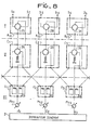
- FIG. 1 represents a supply device in accordance with the invention, supplying a certain number of elementary groupings Ro into which the sub-networks are divided.
- the elementary groupings are characterized by the relatively small number of 2 to 5 or 6 elementary antennas which they comprise.
- N 2 elementary antennas, S i , varying from 1 to n.
- the sub-networks considered are identified by the references R 1 to R 7 and each include 6 elementary antennas. Only 7 sub-networks have been shown, the sub-networks overlapping at their ends being separated from each other by N elementary intervals Do, here therefore 2 Do.
- the elementary groupings are marked Ro 1 to Ro 4 and constitute a set 1. Each elementary grouping has an equal number of inputs and outputs. Here this number N is equal to 2.
- the sets II and III constitute the means bringing together a certain number of the elementary groups Ro, according to the invention.
- the assembly It includes a certain number of circuits called distributor-adders C 1 to C 4 and the assembly III comprises a number of circuits called distributor-dividers F 1 to F 3 which are each connected by a phase shifter Ph to a distributor of energy 3 whose corresponding outputs are spaced by 2 elementary spacings Do.
- the sets II and III bring together MN elementary antennas, that is to say here 6 antennas, M being equal to 3 and N to 2.
- the supply of the antennas with several separate supplies takes place as follows.
- the distributor-divider circuits F 1 , F 2 , F 3 each have 1 input, 3 outputs, and distribute the energy delivered by the distributor 3 respectively to the three inputs of the adder distributor circuits C 1 , C 2 , C 3 . C 4 , the two outputs of which supply an elementary group respectively, here Ro i , Ro 2 , Ro 3 , R 04 .
- the number of outputs of a distributor-divider circuit is equal to the number of inputs of a distributor-adder circuit and that each output of a distributor-divider F 1 for example is connected to an input bearing the same index numeral of successive adding divisors; thus output 1 of circuit F 1 is connected to input 1 of circuit C 1 , output 2 of circuit F 1 is connected to input 2 of circuit C 2 , output 3 of circuit F 1 is connected to l input 3 of circuit C 3 , output 1 of circuit F 2 is connected to input 1 of circuit C 2 , output 2 of circuit F 2 is connected to input 2 of circuit C 3 and output 3 of circuit F 2 is connected to input 3 of circuit C 4 and so on for circuit F 3 .
- the antennas of an elementary group belonging to several sub-networks for example, the antennas of the groups Ro 3 and Ro 4 belonging to the sub-networks R 2 , R s , R 3 , R 7 , R 6 receive several separate feeds.
- FIG. 2 represents a supply device according to the invention, supplying a certain number of elementary groups Ro 1 to R 07 with 2 antennas in which the sub-networks are divided.
- the sub-networks considered here are identified by the references R 1 and R 2 and they are separated by N elementary intervals Do, here therefore 2Do.
- Each elementary grouping has an equal number of inputs and outputs.
- this number N is equal to 2.
- the set II groups together the distributor distributor circuits C 1 to C 6 , gathering a certain number of elementary groupings grouping together M.
- N elementary antennas that is to say here 12 antennas, M being equal to 6.
- the assembly III groups distributor-divider circuits F 1 to F 3 each comprising an input connected to a phase shifter Ph and M outputs.
- the phase shifters Ph 1 and Ph 3 for example, already reduced in number, are connected to an energy distributor 3 whose corresponding outputs are spaced by N elementary spacings Do.
- Each distributor-divider circuit F i has a number of outputs equal to the number M of the inputs of the distributor circuits -adders C i envisaged and each output is connected to an input of the same rank of the successive distributor-adder circuits carrying out a periodic connection law.
- the output 1 of circuit F 1 is connected to the input 1 of circuit C 1
- the output 2 of circuit F 1 is connected to input 2 of circuit C 2
- the output 3 of circuit F 1 is connected to the input 3 of circuit C 3 and so on until the output 6 of circuit F 1 which is connected to input 6 of circuit C 5 .
- the output 1 of the circuit F 2 is connected to the input 1 of the circuit C 2
- the output 2 of the circuit F 2 is connected to the input 2 of the circuit C 3
- the output 3 of the circuit F 2 is connected at input 3 of circuit C 4 and so on.
- the output 1 of circuit F 3 is connected to the input 1 of circuit C 4
- the output 2 of circuit F 3 is connected to input 2 of circuit C 4 and so on.
- circuit F 1 The output 1 of circuit F 1 is connected to the input 1 of circuit C 1 , the output 2 of circuit F 1 is connected to input 2 of circuit C 2 , the output 3 of circuit F 1 is connected to input 3 of circuit C 3 and its output 4 is connected to input 4 of circuit C 4 .
- circuit F 2 the connections are as follows: its output 1 is connected to input 1 of circuit C 2 , its output 2 is connected to input 2 of circuit C 3 , its output 3 to input 3 of circuit C 4 and its output 4 to input 4 of circuit C 5 .
- circuits F 3 and F 4 The connections of the outputs of circuits F 3 and F 4 with the inputs of circuits C are made in the same way, the output 1 of circuit F 3 being connected to input 1 of circuit C 3 and the output 2 of circuit F 4 for example being connected to input 2 of circuit C 5 .
- FIG. 4 represents a supply device according to the invention, for which each elementary grouping Ro i comprises four elementary antennas.
- the sub-networks R 4 and R 5 then each comprise 20 antennas.
- the number M of group interconnection circuits must be greater than the number N of the elementary antennas of the elementary sub-networks. Under these conditions, N being chosen equal to 4, M must be equal to at least 5 and the number of antennas of a sub-network is equal to MN or 20. These sub-networks are spaced from NDo, or four elementary intervals Do.
- the number of group II distributor-adders circuits is equal to 5 and each has five inputs and four outputs, these being respectively connected to the four inputs of the elementary groupings.
- the distributor-divider circuits F each of which is connected to the energy distributor 3 by a phase shifter Ph, therefore have one input and five outputs distributed as follows to the distributor-adder circuits II.
- the output 1 of circuit F 1 is connected to the input 1 of circuit C 1
- the output 2 of circuit F 1 is connected to input 2 of circuit C 2
- the output 3 of circuit F 1 is connected to input 3 of circuit F 3 , output 4 to input 4 of circuit C 4 , etc.
- output 1 of circuit F 2 is connected to input 1 of circuit C 2 , output 2 to input 2 of circuit C 3 , etc.
- the connections of the outputs of circuits F 3 , F 4 and F 5 are made according to the same diagram with the inputs of circuits C 4 , C 5 , C 6 . It will also be noted that the phase shifters Ph are separated by four elementary intervals.
- the limits of the scanning ranges obtained are given with a number of antennas varying from 8 to 44, for given elementary intervals increasing between two elementary antennas and a number varying from 2 to 4 for the elementary groupings considered. It will be noted the advantage of having the largest possible interval between two elementary antennas which results in a lower density of elementary antennas or radiating sources.
- the minimum number of antennas and phase shifters is a function of the interval between elementary antennas and the number of antennas in the elementary grouping.
- FIG. 5 represents a supply circuit of an elementary group comprising two antennas S 1 and S 2 connected by a hybrid circuit 4 to attenuator circuits 5 and 6 having respectively a certain weight A 1 .
- B 1 themselves connected to the inputs E 1 and E 2 by means of a hybrid circuit 7.
- the two separate feeds which are obtained for each of the two antennas S 1 and S 2 can be schematized in the way next:
- the antennas S 3 and S 4 receive under these conditions the sum of the signals from each of the inputs.
- the coefficients A 1 and B 1 representing the weight of the circuits 5, 6, 13, 14, 15 and 16, it is possible to obtain the desired distribution on the antennas.
- the following table gives for each of the antennas S 1 to S 6 considered the distribution of the amplitudes as a function of the coefficients A 1 and B 1 .
Landscapes
- Variable-Direction Aerials And Aerial Arrays (AREA)
Applications Claiming Priority (2)
| Application Number | Priority Date | Filing Date | Title |
|---|---|---|---|
| FR8217917A FR2541518A1 (fr) | 1982-10-26 | 1982-10-26 | Dispositif d'alimentation d'une antenne reseau a faisceau de balayage |
| FR8217917 | 1982-10-26 |
Publications (2)
| Publication Number | Publication Date |
|---|---|
| EP0108670A1 EP0108670A1 (fr) | 1984-05-16 |
| EP0108670B1 true EP0108670B1 (fr) | 1988-09-21 |
Family
ID=9278610
Family Applications (1)
| Application Number | Title | Priority Date | Filing Date |
|---|---|---|---|
| EP83402025A Expired EP0108670B1 (fr) | 1982-10-26 | 1983-10-18 | Dispositif d'alimentation d'une antenne réseau à faisceau de balayage |
Country Status (6)
| Country | Link |
|---|---|
| US (1) | US4692768A (OSRAM) |
| EP (1) | EP0108670B1 (OSRAM) |
| JP (1) | JPS5999803A (OSRAM) |
| CA (1) | CA1220544A (OSRAM) |
| DE (1) | DE3378094D1 (OSRAM) |
| FR (1) | FR2541518A1 (OSRAM) |
Families Citing this family (17)
| Publication number | Priority date | Publication date | Assignee | Title |
|---|---|---|---|---|
| DE3680396D1 (de) * | 1985-07-05 | 1991-08-29 | Siemens Ag | Gruppenantenne mit elektronisch phasengesteuerter strahlschwenkung. |
| CA1226934A (en) * | 1986-09-26 | 1987-09-15 | Henry Downs | Reconfigurable beam-forming network that provides in- phase power to each region |
| FR2628265B1 (fr) * | 1987-03-06 | 1990-12-21 | Thomson Csf | Antenne directive a transducteurs multiples notamment pour sonar |
| FR2638573B1 (fr) * | 1988-11-03 | 1991-06-14 | Alcatel Espace | Antenne a balayage electronique |
| US5144322A (en) * | 1988-11-25 | 1992-09-01 | The United States Of America As Represented By The Secretary Of The Navy | Large-aperture sparse array detector system for multiple emitter location |
| US5028930A (en) * | 1988-12-29 | 1991-07-02 | Westinghouse Electric Corp. | Coupling matrix for a circular array microwave antenna |
| DE69033198T2 (de) * | 1989-01-09 | 1999-11-04 | Mitsubishi Denki K.K., Tokio/Tokyo | Mikrowellenschaltungselemente enthaltende integrierte Schaltungsanordnung |
| US4962381A (en) * | 1989-04-11 | 1990-10-09 | General Electric Company | Systolic array processing apparatus |
| FR2663469B1 (fr) * | 1990-06-19 | 1992-09-11 | Thomson Csf | Dispositif d'alimentation a des elements rayonnants d'une antenne reseau, et son application a une antenne d'un systeme d'aide a l'atterrissage du type mls. |
| EP1600202A1 (en) | 2004-05-24 | 2005-11-30 | Nederlandse Organisatie voor toegepast-natuurwetenschappelijk Onderzoek TNO | Method and means for chemically modifying gases of fumes |
| US20070210959A1 (en) * | 2006-03-07 | 2007-09-13 | Massachusetts Institute Of Technology | Multi-beam tile array module for phased array systems |
| GB0622411D0 (en) | 2006-11-10 | 2006-12-20 | Quintel Technology Ltd | Phased array antenna system with electrical tilt control |
| CN101807976B (zh) * | 2009-02-16 | 2015-09-16 | 中兴通讯股份有限公司 | 一种波频处理装置及方法 |
| JP2016506108A (ja) * | 2012-11-26 | 2016-02-25 | アジャンス スパシャル ユーロペエンヌ | アレイアンテナ用のビーム形成回路およびそれを備えるアレイアンテナ |
| US20160218429A1 (en) * | 2015-01-23 | 2016-07-28 | Huawei Technologies Canada Co., Ltd. | Phase control for antenna array |
| US11569575B2 (en) * | 2019-05-10 | 2023-01-31 | Samsung Electronics Co., Ltd. | Low-complexity beam steering in array apertures |
| US11796630B2 (en) | 2021-01-28 | 2023-10-24 | Ay Dee Kay Llc | MIMO channel extenders with associated systems and methods |
Family Cites Families (15)
| Publication number | Priority date | Publication date | Assignee | Title |
|---|---|---|---|---|
| US3368202A (en) * | 1963-07-15 | 1968-02-06 | Usa | Core memory matrix in multibeam receiving system |
| US3518695A (en) * | 1967-09-07 | 1970-06-30 | Collins Radio Co | Antenna array multifrequency and beam steering control multiplex feed |
| US3474447A (en) * | 1968-05-02 | 1969-10-21 | Raytheon Co | Electronically scanned tacan antenna |
| US3573837A (en) * | 1969-06-30 | 1971-04-06 | Us Navy | Vector transfer feed system for a circular array antenna |
| US3680109A (en) * | 1970-08-20 | 1972-07-25 | Raytheon Co | Phased array |
| US3731315A (en) * | 1972-04-24 | 1973-05-01 | Us Navy | Circular array with butler submatrices |
| US3803625A (en) * | 1972-12-18 | 1974-04-09 | Itt | Network approach for reducing the number of phase shifters in a limited scan phased array |
| US4080605A (en) * | 1976-08-26 | 1978-03-21 | Raytheon Company | Multi-beam radio frequency array antenna |
| US4257050A (en) * | 1978-02-16 | 1981-03-17 | George Ploussios | Large element antenna array with grouped overlapped apertures |
| US4228436A (en) * | 1978-04-03 | 1980-10-14 | Hughes Aircraft Company | Limited scan phased array system |
| AU531239B2 (en) * | 1978-06-15 | 1983-08-18 | Plessey Overseas Ltd. | Directional arrays |
| GB2034525B (en) * | 1978-11-17 | 1983-03-09 | Marconi Co Ltd | Microwave transmission systems |
| US4321605A (en) * | 1980-01-29 | 1982-03-23 | Hazeltine Corporation | Array antenna system |
| US4424500A (en) * | 1980-12-29 | 1984-01-03 | Sperry Corporation | Beam forming network for a multibeam antenna |
| US4489325A (en) * | 1983-09-02 | 1984-12-18 | Bauck Jerald L | Electronically scanned space fed antenna system and method of operation thereof |
-
1982
- 1982-10-26 FR FR8217917A patent/FR2541518A1/fr active Granted
-
1983
- 1983-10-18 DE DE8383402025T patent/DE3378094D1/de not_active Expired
- 1983-10-18 EP EP83402025A patent/EP0108670B1/fr not_active Expired
- 1983-10-24 US US06/545,008 patent/US4692768A/en not_active Expired - Fee Related
- 1983-10-25 CA CA000439670A patent/CA1220544A/en not_active Expired
- 1983-10-26 JP JP58199308A patent/JPS5999803A/ja active Pending
Also Published As
| Publication number | Publication date |
|---|---|
| EP0108670A1 (fr) | 1984-05-16 |
| JPS5999803A (ja) | 1984-06-08 |
| DE3378094D1 (en) | 1988-10-27 |
| FR2541518A1 (fr) | 1984-08-24 |
| CA1220544A (en) | 1987-04-14 |
| FR2541518B1 (OSRAM) | 1985-03-08 |
| US4692768A (en) | 1987-09-08 |
Similar Documents
| Publication | Publication Date | Title |
|---|---|---|
| EP0108670B1 (fr) | Dispositif d'alimentation d'une antenne réseau à faisceau de balayage | |
| EP0407243B1 (fr) | Système d'antenne à faisceaux multiples à modules actifs, et formation de faisceaux par le calcul numérique | |
| EP0651461B1 (fr) | Antenne à réseau d'éléments rayonnants | |
| FR2527785A1 (fr) | Procede et dispositif de reduction de la puissance des signaux de brouillage recus par les lobes lateraux d'une antenne radar | |
| FR2729505A1 (fr) | Antenne multifaisceaux forte capacite a balayage electronique en emission | |
| EP0368121B1 (fr) | Antenne à balayage électronique | |
| FR2698212A1 (fr) | Source élémentaire rayonnante pour antenne réseau et sous-ensemble rayonnant comportant de telles sources. | |
| EP0891005B1 (fr) | Antenne réseau antibrouillée | |
| FR2710471A1 (fr) | Diviseur de puissance micro-onde réglable. | |
| FR2693841A1 (fr) | Procédé et appareil de traitement de signaux d'une antenne. | |
| FR3076138B1 (fr) | Procede de couverture multifaisceaux par regroupement de faisceaux elementaires de meme couleur, et charge utile de telecommunications pour mettre en oeuvre un tel procede | |
| WO2014040957A1 (fr) | Antenne multibande à inclinaison électrique variable | |
| FR2491686A1 (fr) | Antenne directive de radar multimode a alimentation double | |
| EP3758146B1 (fr) | Formateur analogique multifaisceaux bidimensionnel de complexité réduite pour antennes réseaux actives reconfigurables | |
| FR2792116A1 (fr) | Formation numerique de faisceaux | |
| EP2363729B1 (fr) | Formateur de voies reconfigurable pour antenne réseau | |
| EP0225219A1 (fr) | Antenne réseau à balayage conique et radar comportant une telle antenne | |
| FR3098364A1 (fr) | Constellation vectorielle multi-echelle | |
| TWI637560B (zh) | 階層式模組化主動式陣列天線系統 | |
| FR2862440A1 (fr) | Architecture d'antenne adaptative multifaisceaux a formation de faisceaux par le calcul | |
| EP2656437A1 (fr) | Circuit formateur de faisceau et système d'antenne comprenant un tel circuit | |
| EP4092831A1 (fr) | Antenne à réseau de distribution lacunaire | |
| FR2632419A1 (fr) | Procede et dispositif d'antibrouillage pour radar et radar equipe d'un tel dispositif | |
| WO1990015342A1 (en) | Power efficient feed network for tacan antenna arrays | |
| EP1698021A1 (fr) | Procede d optimisation de l'architecture d'une antenne multifaisceaux a formation de faisceaux par le calcul (ffc) a sous-reseaux imbriques. |
Legal Events
| Date | Code | Title | Description |
|---|---|---|---|
| PUAI | Public reference made under article 153(3) epc to a published international application that has entered the european phase |
Free format text: ORIGINAL CODE: 0009012 |
|
| AK | Designated contracting states |
Designated state(s): DE GB IT NL |
|
| 17P | Request for examination filed |
Effective date: 19840622 |
|
| 17Q | First examination report despatched |
Effective date: 19860820 |
|
| D17Q | First examination report despatched (deleted) | ||
| GRAA | (expected) grant |
Free format text: ORIGINAL CODE: 0009210 |
|
| AK | Designated contracting states |
Kind code of ref document: B1 Designated state(s): DE GB IT NL |
|
| ITF | It: translation for a ep patent filed | ||
| REF | Corresponds to: |
Ref document number: 3378094 Country of ref document: DE Date of ref document: 19881027 |
|
| GBT | Gb: translation of ep patent filed (gb section 77(6)(a)/1977) | ||
| RAP4 | Party data changed (patent owner data changed or rights of a patent transferred) |
Owner name: THOMSON-CSF |
|
| PLBE | No opposition filed within time limit |
Free format text: ORIGINAL CODE: 0009261 |
|
| STAA | Information on the status of an ep patent application or granted ep patent |
Free format text: STATUS: NO OPPOSITION FILED WITHIN TIME LIMIT |
|
| 26N | No opposition filed | ||
| PGFP | Annual fee paid to national office [announced via postgrant information from national office to epo] |
Ref country code: NL Payment date: 19891031 Year of fee payment: 7 |
|
| PG25 | Lapsed in a contracting state [announced via postgrant information from national office to epo] |
Ref country code: NL Effective date: 19910501 |
|
| NLV4 | Nl: lapsed or anulled due to non-payment of the annual fee | ||
| ITTA | It: last paid annual fee | ||
| PGFP | Annual fee paid to national office [announced via postgrant information from national office to epo] |
Ref country code: DE Payment date: 19940917 Year of fee payment: 12 |
|
| PGFP | Annual fee paid to national office [announced via postgrant information from national office to epo] |
Ref country code: GB Payment date: 19940920 Year of fee payment: 12 |
|
| PG25 | Lapsed in a contracting state [announced via postgrant information from national office to epo] |
Ref country code: GB Effective date: 19951018 |
|
| GBPC | Gb: european patent ceased through non-payment of renewal fee |
Effective date: 19951018 |
|
| PG25 | Lapsed in a contracting state [announced via postgrant information from national office to epo] |
Ref country code: DE Effective date: 19960702 |