EP0107390A1 - Supervised wireless security system - Google Patents
Supervised wireless security system Download PDFInfo
- Publication number
- EP0107390A1 EP0107390A1 EP83305865A EP83305865A EP0107390A1 EP 0107390 A1 EP0107390 A1 EP 0107390A1 EP 83305865 A EP83305865 A EP 83305865A EP 83305865 A EP83305865 A EP 83305865A EP 0107390 A1 EP0107390 A1 EP 0107390A1
- Authority
- EP
- European Patent Office
- Prior art keywords
- frequency
- transmitter
- sensor
- message
- receiver
- Prior art date
- Legal status (The legal status is an assumption and is not a legal conclusion. Google has not performed a legal analysis and makes no representation as to the accuracy of the status listed.)
- Withdrawn
Links
Images


Classifications
-
- G—PHYSICS
- G08—SIGNALLING
- G08B—SIGNALLING OR CALLING SYSTEMS; ORDER TELEGRAPHS; ALARM SYSTEMS
- G08B25/00—Alarm systems in which the location of the alarm condition is signalled to a central station, e.g. fire or police telegraphic systems
- G08B25/01—Alarm systems in which the location of the alarm condition is signalled to a central station, e.g. fire or police telegraphic systems characterised by the transmission medium
- G08B25/10—Alarm systems in which the location of the alarm condition is signalled to a central station, e.g. fire or police telegraphic systems characterised by the transmission medium using wireless transmission systems
-
- G—PHYSICS
- G08—SIGNALLING
- G08B—SIGNALLING OR CALLING SYSTEMS; ORDER TELEGRAPHS; ALARM SYSTEMS
- G08B25/00—Alarm systems in which the location of the alarm condition is signalled to a central station, e.g. fire or police telegraphic systems
- G08B25/007—Details of data content structure of message packets; data protocols
Definitions
- the present invention relates to a security alarm system incorporating a radio communication link between remote sensors and a central security monitoring device.
- Radio-linked security alarm system which is low in cost, provides an extended period of operability without maintenance, whose transmitters are small enough for convenient installation, in which frequent reassurance of the op - erability of each transmitter is provided, and wherein positive identification of the location of an intrusion is provided automatically by the transmitter unit.
- the aforementioned disadvantages of previously known wireless alarm systems are overcome by the present invention, which provides a low cost wireless alarm system and a method for communicating a dependable supervised one-way flow of information from remote sensors using a single transmission pathway to provide frequent, individually identifiable indications of the status of each of a plurality of sensor devices, as well as the status of the transmitter associated with each sensor device.
- the invention provides transmitters which are of small size, require a very small average current, and are operable for long periods of time without the necessity for maintenance.
- the wireless alarm system of the invention incorporates a supervisory technique and apparatus by which it becomes apparent within a predetermined time when one or more of the transmitters requires maintenance, and by which the identity of a particular transmitter unit requiring maintenance is made known.
- a receiver-decoder and a plurality of encoder- equipped transmitter units are presettable to establish digitally encoded system and channel addresses, and a receiver-decoder of that system rejects signals from transmitters of similar systems operating nearby enough for reception by the receiver-decoder.
- the decoder section of the receiver-decoder accepts those messages received by the receiver portion only if the messages contain the correct digitally encoded system address, rejecting all other messages.
- Each message accepted by the decoder is checked for validity and only if valid is the message routed according to its digitally encoded channel address to a corresponding channel within the receiver-decoder.
- each channel address code is assigned to only one transmitter unit, and each message acceptable to the receiver-decoder is thus identifiable by its channel address code as having originated from that particular transmitter unit and its associated sensor.
- Each message includes, in addition to the system and channel address codes, an indication of the output of the sensor associated with the particular transmitter which has sent the message, for example a door-operated switch which indicates whether a door is open or closed, a fire or smoke detector, or a manually operable portable switch for medical alert purposes.
- the particular channel receives, decodes, and provides an indication of the digitally encoded status data relating to the condition detected by the particular sensor.
- Receipt of a valid message regardless of the sensor data included in the message, resets a timer which relates to that particular channel in a maintenance warning portion of the receiver-decoder. Failure to receive a message allows a preset time to elapse, after which a maintenance requirement warning indication is provided. In this manner periodic transmission from each transmitter gives frequent reassurance of the operability of each individual transmitter.
- each transmitter broadcasts a very brief message which includes system address, channel address, and sensor data, all in coded form.
- each coded message includes address and sensor data sent twice in sucoes- sion, the duplication permitting the decoder portion of the system to validate the message received.
- the duty cycle ratio of each individual transmitter is so low, and the inter-transmission period is sufficiently different among the individual transmitters, that it effectively precludes statistically significant mutual interference among the transmitters of such a system.
- the length of each individual message is short enough so that the individual transmitters each transmit a report frequently enough to be substantially equivalent to fully continuous "supervision" of the individual transmitters.
- the low duty cycle also extends the life of the batteries of the transmitter units, and thereby extends the time during which the system will operate without maintenance, as well as reducing the size of the batteries required, and thereby reducing the overall size of each transmitter unit.
- FM radio communication is used in the alarm system of the present invention in order to obtain a high signal/ noise ratio, while reducing transmitter and receiver complexity.
- An added feature protects the communication link against frequency drift which may afflict components which operate over a long period of time.
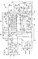
- FIG. 1 shows security alarm systems 10 and 12, which embody the present invention, in block diagram form.
- Sensors such as a door switch 14, a window switch loop circuit 16, a personal portable switch 18, and a fire sensor 20 are associated respectively with transmitters 22-28.
- the door switch 30 is associated with a transmitter 32 in the alarm system 12.
- the alarm systems 10 and 12 include respective receiver-decoders 34 and 36, each of which includes indicators such as the audible alarm 38, the visual alarm display 40, and the maintenance warning indicators 42.
- An automatic telephone dialer 44 may also be connected to the receiver-decoder 34.
- each of the transmitters 22-28 and 32 are of identical construction and transmit on the same nominal transmitter frequency.
- the receiver-decoders 34 and 36 are tuned to receive transmissions in that same frequency band.
- the transmitter 22 may be seen to comprise a voltage controlled variable frequency oscillator 50.
- An encoder 54 which may be an integrated circuit, and a lock-on pulse generator circuit 56 provide controlling voltages to the voltage controlled variable frequency oscillator 50 by way of a low-pass filter (LPF) 52.
- a power supply such as a battery BT provides power through a power supply switch circuit 58 to the variable frequency oscillator 50, and through a voltage doubler 59 to another part of encoder 54 and to a lock-on pulse circuit 56 to initiate transmission of a message each time an appropriate signal is provided to the power supply switch circuit 58 by either a timer circuit 60 or a sensor switch circuit 62.
- the signal from the power supply switch circuit 58 is also provided to a transmit enable circuit 64 which signals the encoder 54 to initiate transmission of a message.
- the encoder 54 in response, provides an information-carrying sequence of voltage pulses to the voltage controlled variable frequency oscillator 50, by way of the low-pass filter 52, and, for the duration of each transmission, provides a signal, through a hold-on circuit 66, to the power supply switch circuit 58, retaining the power supply switch circuit 58 in its .”on" condition.
- An alarm switch 67 responds to the state of the sensor switch circuit 62, providing an input voltage enabling the encoder 54 to generate a data character reporting the status of the sensor switch as a part of each transmitted message.
- a battery power supply BTl, BT2 comprises a pair of "AAA" 1.5-volt alkaline cells connected in series, at least theoretically capable of powering the transmitter 22 for as long as several years.
- the timer circuit 60 is a multi-vibrator circuit including transistors Ql, Q2, which provides an enabling pulse to the turn-on switch circuit 58 through capacitor C3 and resistor R5, at intervals of approximately 35 seconds. This pulse provides a voltage across resistor R6, turning on transistor Q3 in the turn-on switch circuit 58.
- transistor Q3 When transistor Q3 turns on, the voltage at its collector rises to the voltage of the battery.
- the collector voltage of transistor Q3 is supplied across the transmit enable circuit 64 with current through the resistors R9 and R10 turning on transistor Q4 and presenting a ground potential or low voltage signal at a - transmission enabling terminal TE of integrated circuit Ul of encoder circuit 54, during the time required to charge the capacitor C5.
- the encoder 54 comprises an integrated circuit Ul, for example integrated circuit MC145026PD manufactured by Motorola Semiconductor Products, Inc., and switch SW1, for example a double in-line package switch having twelve single pole, single throw (SPST) switches, which may be preset to control the output of the encoder.
- SPST single pole, single throw
- Each set of poles of the switch SW1 associated with a respective terminal A l -A4 has a possibility of three different settings, providing a total of 81 separate trinary encoded combinations, known as address codes.
- An address code serves to identify a particular alarm system.
- the SW1 poles associated with terminals D 5 -D 8 may each be set in an open or closed position to provide sixteen separate binary combinations known as channel codes. A separate channel code is assigned to each transmitter in a particular alarm system.
- the integrated circuit Ul is an encoder which will produce a nine-cell data word in serial format.
- Ul provides two successive, identical data words out of terminal D ou t.
- the cells of each data word correspond to the input terminals A l -A4 and D 5 -D 9 according to the following relationship, beginning with the first cell:
- Data word AlA2A3A4D5D6D7D8D9
- Each cell contains one digital character selected from the set characterized as containing the characters "open,” "one,” and "zero.” The character is selected by the state of the device connected to the corresponding input terminal.
- terminals A 1 -A4, as shown in FIG. 3 are set, respectively, to produce characters zero, one, open, and open.
- Terminals D 5 -Dg as shown, are set, respectively, to produce 25 characters zero, open, zero, and open.
- the transmit enable terminal TE in the encoder integrated circuit Ul accepts pulses from the transmission-enabling circuit 64.
- Input terminal D9 accepts information from the sensor switch circuit 62 to provide a character for the 9th cell in each data word of the message format of the encoder 54.
- Terminals R tc , C tc , and R s are interconnected by a network including resistor R15, capacitor C9, and resistor R16 to set the frequency of an internal clock of the integrated circuit Ul, which is established as 75 Kilohertz in the embodiment shown.
- Terminal D out of the integrated circuit Ul produces, in a serial stream, the two-word output assembled according to the format described above, in voltage pulse, digital signal form. This output is provided through R14 to the low pass filter network 52.
- the voltage doubler circuit 59 includes a high potential side having a resistor R7 connected between the positive terminal of the power supply and the side of capacitor C4 opposite the collector of transistor Q3.
- the size of capacitor C4 is chosen to maintain the voltage across capacitor C4 nearly constant for the duration of each transmission.
- the combination of transistor Q3, resistor R7 and capacitor C4 thus provides approximately six volts between terminals Vdd and Vss of integrated circuit Ul.
- a transistor Q7 whose base is connected to ground through a resistor R12 in series with a capacitor C7.
- a resistor R13 is connected between the base of transistor Q7 and its emitter, which is connected to the positive side of capacitor C4.
- the collector of transistor Q7 is connected, through resistor R18, to the low-pass filter network 52.
- the sensor switch circuit 62 includes switch SW31, which provides an electrical response to an actual sensed condition, such as whether a door is open.
- the condition of switch SW31 is communicated to the alarm bit switch 67, which in this embodiment comprises a transistor Q5 connected to provide an appropriate electrical signal to terminal D9 of the encoder Ul.
- Switch SW31 connects the base of the transsistor Q5 through resistor Rll alternatively to a ground potential through resistor R32, or power supply voltage, through resistors R6, R31, and R32.
- a capacitor C31 is charged when switch SW31 is in a normal, or "door closed" position, one side of capacitor C31 being connected to resistor R31 and the other side to a junction between resistors R32 and Rll. Also connected to the junction between resistors R32 and Rll is one side of a capacitor C32, whose other side is connected to ground.
- transistor Q3 when transistor Q3 is turned on, the voltage on capacitor C4 and at terminal V dd of integrated circuit Ul, rises to approximately six volts.
- the current through transistor Q3 charges C5, turning on transistor Q4, and a transmission-enabling low pulse is provided from the transmission-enabling circuit 64 to the terminal TE of integrated circuit Ul, activating the encoder circuit 54.
- the encoder circuit 54 Once the encoder circuit 54 is activated it proceeds through its programmed routine, and then shuts down. During this time the hold-on circuit 66 keeps transistor Q3 turned on to provide power to the encoder circuit 54 and the variable frequency oscillator 50.
- the hold-on circuit 66 includes transistor Q6, whose base is connected through resistor R17 to terminal C tc of integrated circuit Ul, and whose collector is connected through resistor R8 to the base of transistor Q3 of the power supply switch circuit 58.
- Transistor Q6 is turned on by the voltage across R17 with each positive excursion of the internal clock output terminal C tc of Ul. This action discharges C8, thus supplying a substantially constant current through R8 to the base of Q3 for the period of time utilized by Ul to generate its two-word output message, after which the internal clock is disabled.
- Variable frequency voltage controlled oscillator circuit 50 comprises, preferably, a series tuned Colpitts type radio frequency oscillator, chosen because of its simplicity and stability.
- the instantaneous actual oscillator frequency is determined by the complex reactance of the network comprising RF coil Ll, capacitors C13, C14, C15, and the junction capacitance of diode D20.
- This frequency is modulated by application of control voltage pulses from the collector of transistor Q7 and from the D out terminal of integrated circuit Ul, through the low-pass filter 52, to the voltage-controlled variable capacitance diode D20 whose junction capacitance changes with changes in its junction voltage. This change in capacitance in turn modulates the reactance, and, thus, the frequency of oscillation of the oscillator 50.
- the nominal center frequency of the preferred embodiment is 314 MHz, which may vary slightly with variations in element characteristics: the frequency deviation of the transmitter of the preferred embodiment is +2.5 MHz.
- the voltage-controlled diode D20 is connected to ground and in series with the low-pass filter 52.
- the low-pass filter includes a resistor R18 whose high voltage side is connected to the collector of transistor Q7 of the lock-on pulse generator circuit 56 and, through resistor R14, to the terminal D out of the integrated circuit Ul.
- a capacitor C10 is also connected, in parallel with the resistor R18 and diode D20, between Q7 and ground.
- the capacitor C14 has one side connected to a point between resistor R18 and diode D20, while its other side is connected to the emmitter of transsistor Q8 of the oscillator 50.
- the effect of the low-pass filter 52 is to slow the rise and fall times of the output voltage of the D ou t terminal of the encoder Ul to about 2 microseconds each, a rate producing a frequency change in the oscillator's output which can be tracked by a receiver including a suitable automatic frequency tracking circuit.
- the RF output of the voltage-controlled oscillator circuit 50 is allowed to radiate from the circuit elements, unaided by an antenna. This helps reduce the size of the transmitter 22. It is understood, however, that an antenna may be employed with the transmitter 22 to radiate the RF output.
- FIG. 4 illustrates the frequency output of oscillator 50 with time.
- Q3 is activated by the timing circuit 60
- oscillator 50 turns on and lock-on circuit 56 provides the "lock-on" pulse through diode Dl in the manner described above which causes the frequency of the oscillator 50 to vary accordingly.
- the TE terminal of the integrated circuit Ul is pulsed by transmit enable circuit 64.
- M145026PD which comprises Ul in the preferred embodiment
- a preliminary period equivalent in time to two data characters, passes before the first data word is output from terminal D ou t of Ul.
- the Motorola device then provides as an output from terminal D out two successive, identical data words, with a three-character time space separating the pair.
- this output which swings between ground and the voltage at terminal V dd , is provided through the diode D20 to the oscillator 50, the effect on the frequency oscillator 50 output is clearly shown in FIG. 4.
- integrated circuit Ul automatically shuts off itself and, through hold-on circuit 66, the rest of the transmitter 22 as described hereinabove.
- FIG. 3A depicts a switch circuit which can be substituted for the sensor switch circuit 62 of the FIG. 3 circuit by connecting each circuit point X, Y, BT and ground to its identically designated corresponding point in the FIG. 3 circuit.
- a switch, SW61 which can comprise, for example, a push-button mechanism in a hand-held transmitter serving as a personal emergency alarm, is depressed, which discharges capacitor C61 through R63. This turns on transistor Q61, activating a timing circuit which includes transistors Q62 and Q63.
- the values of the timing circuit elements are selected to cause the circuit to oscillate with a period considerably less than the period of timer circuit 60.
- the values of resistors R65-68 and capacitors C62 and C63 are selected to cause Q3 and the rest of transmitter 22, through circuit connection X, to be switched on every 0.16 seconds. This oscillation will be maintained until switch SW61 is opened, and after that, for the period of time, determined by the values of R61, R62, and C61, required to charge up C61. While switch SW61 is closed, and thereafter for the period of time required to charge C61, the collector voltage of transistor Q61, through circuit connection Y, activates the alarm bit switch 67 and causes the alarm status encoded at terminal D9 of integrated circuit Ul to be set. Thus, closing switch SW61 will increase the rate of transmission and cause each transmission occurrance in the speeded - up sequence to carry an alarm indication.
- FIG. 3B depicts a circuit for sensing the state of a switch series loop L40 connected between terminals T 41 and T 42 .
- the switch loop L40 can comprise, for example, a circuit connecting in series the window and door sensor switches in a single room or group of rooms.
- the circuit of FIG. 3B is connected at points X, Y, BT, and ground, respectively, to the identically-designated points in the circuit shown in FIG. 3.
- the loop opens and capacitor C41 is charged toward the potential of BT through resistor R41.
- the current through R41 turns transistor Q41 on.
- Q41 turns on, its collector goes to ground which turns off the transistor pair Q42 and Q44, which have kept point Y at ground and Q5, the alarm bit switch of FIG.
- transistor Q41 turns on, transistor Q43 turns on quickly through resistor R47 and capacitor C42 because the value R42 is several orders of magnitude less than that of resistor R46. After C42 is charged, base current for Q43 is supplied through R46. The speed of Q43's switch into operation causes circuit point Y to 1 1 e quickly driven positive. This quick excursion is fed buck to transistor Q41 through resistor R53, which speeds up the operation of Q41. The shift into operation of transistor Q43 causes capacitor C44 to discharge and capacitor C45 to charge, which causes current to flow through circuit point X, creating a voltage drop across resistor R6 of FIG. 3. The R6 voltage drop activates transistor Q3 and, with it, transmitter 22.
- circuit point Y is driven positive which causes the alarm bit switch transistor Q5 to turn on, providing an alarm indication to integrated circuit U1.
- the switch circuit of FIG. 3B turns on the transmitter 22 and causes it to transmit an alarm indication.
- the alarm indication will remain set because transistor Q5 of the transmitter 22 will remain on through the operation of transistors Q41 and Q43 of the FIG. 3B circuit.
- Table I shows the values and types of components of the exemplary transmitter 22 shown in FIG. 3 and switch circuits shown in FIGS. 3A and 3B.
- the receiver-decoder 34 is shown in block diagram form in FIG. 5 and schematically in FIGS. 6 and 7.
- the receiver 68 portion may be seen to comprise a receiver antenna 70, a 10 MHz bandwidth band-pass filter 71 tuned to a 314 MHz center frequency, a wide-band radio frequency (RF) mixer 72, a narrow-band intermediate frequency (IF) band-pass filter 73 with a 2 MHz bandwidth, an IF amplifier 74, and an IF FM detector circuit 76.
- a frequency signal representing the difference between the voltage-controlled oscillator frequency and the received signal frequency, is passed through the IF band pass filter 73 from the wide-band RF mixer 72 for amplification in the narrow-band IF amplifier 74.
- a frequency feedback output voltage from the FM detector circuit 76 a voltage which is higher with a higher received signal frequency and lower with a lower received signal frequency, is provided through a dc-coupled amplifier 78 to modulate the output frequency of a voltage-controlled variable frequency local oscillator 80.
- the frequency feedback voltage corresponding to any change in the frequency of the RF signal, thus controls the difference frequency output by the RF mixer 72, allowing the receiver 68 to follow the RF signal of the transmitter 22 even though its frequency varies over a range greater than the IF section bandwidth.
- the amplified signal detected in the detector 76 is also provided to the decoder 82 by way of a dc level restorer amplifier 81.
- the frequency variations transmitted by the transmitter 22 amount to serially encoded digital data characters forming a message consisting of two 9-cell words.
- the decoder circuit reads and remembers the first word, compares the second word to the first word, and if the two words are identical converts the last five characters of data in the word, corresponding to the states of terminals D5-9 of the transmitter encoder integrated circuit Ul, from serial to parallel form.
- the fifth through eighth characters of data in each word provide a channel address in binary coded form, allowing a choice of sixteen separate channel addresses.
- the final character of each word is the sensor status data character which indicates whether the switch SW1 is in the "normal" or "alarm" position.
- a signal is provided to the proper one of the sixteen parallel channels of both a matinenance warning circuit 84 and an alarm indicator circuit 86. Receipt of such a signal in any particular channel resets a timer circuit in the respective channel of the maintenance warning circuit 84, preventing a matinenance warning from being produced by the receiver-decoder 34.
- FIG. 6 shows schematically a receiver circuit 88 which is tunable to a nominal radio frequency of 314 Megahertz, compatible with the transmitter circuit 22 shown in FIG. 3.
- the RF signal received through the antenna 70 is filtered and mixed with a signal produced in the local voltage-controlled variable frequency oscillator 80, the difference between the two frequencies being passed through a tuned band-pass coupling transformer filter 73 into the intermediate frequency amplifier 74 comprising a pair of integrated circuits U2, U3 and thence into the detector 76.
- the band-pass filter 73 is tuned to 20 MHz, with a bandwidth of 2 MHz, allowing only RF signals whose frequency is very close to the actual instantaneous frequency of the transmitter 22 to be amplified and detected.
- An output signal from the IF detector 76 is amplified and provided as a feedback to modulate the frequency of the local oscillator 80.
- the signal is also amplified in the dc level restorer amplifier 78 and provided at the data output terminal 90.
- the dc level restorer centers the amplified output of the detector on the input transfer characteristic of transistor Q13 which acts as a slicing amplifier to provide a voltage pulse digital signal which can be handled by the decoder 82.
- Table II lists exemplary components of the receiver circuit 68 of FIG. 6.
- the data provided by the receiver 68 as its output is processed in the decoder 82 to determine whether the signal received is relevant to the alarm system 23, whether it contains a valid message, and to determine what sensor status has been reported in the message.
- the decoder circuit 82 shown schematically in FIG. 7, includes an integrated circuit U4.
- the circuit U4 is a Motorola MC145027, modified by the manufacturer to provide four address terminals A l -A4 and five data terminals D 5 -D 9 for the purposes disclosed herein.
- a presettable address encoding switch SW3 is connected to address data terminals A 1 -A 4 of integrated circuit U4.
- any received message which contains the proper combination of data characters matching the selected settings of the address encoding switch SW3 is processed by reading and storing the additional five characters of data in the first word. If the second word is identical to the first word received, the integrated circuit U4 passes on the combination of characters from its data output terminals D l -D 4 to provide the identification of the particular channel, within the alarm system 12, .whose transmitter has sent a message. This channel identification information is transmitted through a gate circuit U5 to two pairs of integrated circuits, included respectively in the maintenance warning circuit 84 and the alarm indicator circuit 86. Each time a valid message is received for a particular channel the integrated circuits U6 and U7 provide a resetting pulse to the appropriate one-shot timer circuit 92, of which one is provided for each channel. The timer circuits 92 count down at a frequency established by the integrated circuit U10. So long as a valid signal is received on each channel, resetting the associated circuit 92 within a predetermined time, the maintenance warning circuit 84 interprets the situation as being normal.
- the resepctive timer circuit 92 switches on, providing power to the appropriate maintenance warning light emitting diode 94. This causes the respective diode 94 to light, indicating which of the sixteen channels is experiencing a malfunction, and also turns on transistor Q15 whose output is connected to provide an optional audible warning that maintenance is required in the system.
- a switch SW4 for each channel permits that channel's one-shot timer 92 to be disconnected from the associated LED 94 and from the transistor Q15.
- the four channel-identifying data characters are also provided to the pair of integrated circuits U8 and U9, which similarly read the combination of characters provided from terminals D1-D4 of the integrated circuit U4 and provide an output to the appropriate channel's alarm circuit. Also provided to each of the integrated circuits U8 and U9 is the final character of each nine-cell word received, providing an indication of the sensor status reported. So long as the sensor status is normal, corresponding to a "normal" position of switch SW1 in the particular transmitter 22 which has sent the message received and decoded, no output will be provided to any of the channels from the integrated circuits U8 and U9.
- the output on that particular channel goes high and latches there until reset by a "normal” message or by a manual indicator reset switch SW6.
- the channel outputs of U8 and U9 can also be reset by a manual alarm reset switch SW5 connected with terminals of U8 and U9.
- the high output on an output channel of U8 or U9 lights an associated light emitting diode 96 and turns on an associated transistor Q16, Q17, Q18, or Q19, whose collector current then actuates an appropriate one of the relays 98, 100, 102, or 104 to initiate a predetermined course of action, such as actuating an automatic telephone dialer 44 or an audible fire or burglar alarm 38.
- Table III lists exemplary components of the decoder of FIG. 7.
- each system address code provides a choice of up to 81 systems such as the alarm systems 10 and 12, each containing 16 channels, which may be selected using the settings of contacts 9-12 of transmitter switch SW1 to provide channel identification in the message transmitted by each transmitter 22, with each transmitter 22 being capable of reporting a normal or alarm condition using the final data character of the nine-cell word automatically transmitted by the encoder Ul.
- the internal clock frequency of the integrated circuit Ul determined by the combination of R15, C9, and R16 is preferably at least 75 KHz, and the entire message is transmitted in a period of approximately 0.0025 seconds or less. A transmission is followed by a non-transmitting period of approximately 35 seconds established by the timer circuit 60, giving an operating duty cycle ratio of no more than about one in 14,000 for any one transmitter. Because of the random difference between the transmission periods initiated by the timer circuits of different transmitters 22, the result is a very low likelihood of interference between any two transmitters 22 in any one system 10 or 12 even though all of the transmitters 22 are operating on the same nominal radio frequency, unless more than one transmitter 22 is assigned the same channel address code.
- the duty cycle may be substantially higher than this figure and may be changed, for example, to as high as one in 100 by speeding up the timer circuit 60 and changing the internal clock rate of the integrated circuit Ul.
- each transmitter adjusted to provide a relatively high duty cycle of one in 100, as by scheduling a 0.1 second transmission every 10 seconds, there is only one chance in 12.5 that the first transmission of any one transmitter will be blocked, and one in 156 that the second scheduled transmission 10 seconds later would overlap the transmission of another transmitter.
- the intermediate frequency amplifier is tuned to receive signals within a much narrower frequency bandwidth of only 2.0 Megahertz, less than 50% of the full 5 Megahertz frequency shift due to the +2.5 MHz frequency deviation.
- the lock-on pulse generated at the beginning of each trans mission from each transmitter includes a sweep of the actual instantaneous oscillator frequency passing relatively slowly through the nominal frequency to which the receiver is tuned, to give the receiver an opportunity to detect the transmitted signal and begin tracking the variations of transmission frequency which contain the system address, channel address, and status data in frequency modulated digitally encoded format.
- the range of the initial frequency ramp provided by the transmitter extends from approximately 2.5 Megahertz (0.8%) above the inherent actual center frequency of the oscillator to 2.5 Megahertz (0.8%) below the inherent actual center frequency of the oscillator.
- the frequency ramp ensures that the frequency of the transmission will pass through the tuned nominal frequency of the receiver, even though the transmitter oscillator's actual frequency may shift by as much as 0.8% as a result of temperature shifts, supply voltage variations, or changes of the characteristics of its electronic components during its lifetime.
- the present invention teaches, then, avoiding interference among a plurality of transmitter units in a wireless security alarm system and avoiding interference among a plurality of similar systems, all operating in a single radio frequency channel, by periodically transmitting from each transmitter a message whose length is as short as practicable, but certainly less than 1/10 of a second, and thereafter waiting for a period of at least 10 seconds as required by government regulations.
- This method avoids interference between transmitters by the use of an extremely low duty cycle ratio while still transmitting frequently enough to provide assurance of transmitter operability, to reduce the likelihood of transmission by more than one transmitter in the reception area during the same time to a statistically insignificant value.
- the invention comprises transmission of information using a digitally encoded frequency modulation keyed message format, receiving each transmission by the use of a receiver which has an intermediate frequency section whose bandwidth is narrower than the received signal frequency deviation, and which locks onto the tracks the changing frequency of the transmitted signal.
- the present invention teaches a method of continually verifying that each transmitter of a wireless alarm system according to the invention remains operable, by providing a maintenance warning whenever the time since the last valid signal from any single transmitter unit of the system exceeds a predetermined value and by using digitally encoded system address and channel address information to identify specifically which transmitter has sent a particular message or has failed to send any message.
Landscapes
- Engineering & Computer Science (AREA)
- Computer Networks & Wireless Communication (AREA)
- Business, Economics & Management (AREA)
- Emergency Management (AREA)
- Physics & Mathematics (AREA)
- General Physics & Mathematics (AREA)
- Alarm Systems (AREA)
Abstract
Apparatus and method for communication by use of a single FM radio frequency, from a plurality of transmitters to a central receiver in a security alarm system or similar system. A transmitter's radio frequency signal is modulated in wide frequency swings to transmit digitally encoded address, subaddress, and sensor status information in a very brief format. A transmission is provided periodically from each transmitter, but a very low duty cycle is used to avoid interference among the transmitters. A transmitter frequency sweep provides the receiver an opportunity to lock onto a transmission before data is transmitted. Thereafter the receiver automatically tracks the rapidly varying frequency of the transmitted signal. Address and subaddress data identify each transmission and a maintenance warning ir provided by the receiver-decoder unit to identify any transmitter which fails to reportwithin a predetermined time. Each significant sensor status change initiates a transmission from the related transmitter. Low duty cycle and low transmitter power requirements provide long transmitter battery life.
Description
- The present invention relates to a security alarm system incorporating a radio communication link between remote sensors and a central security monitoring device.
- It has long been considered desirable in an alarm system to use a radio communication link between the remote sensors, such as door switches, window switches, manually-operable personal emergency signal switches, and the like, and a central security monitoring and alarm-signaling device. The potential advantages of such a system include avoiding the expense of installing wiring between remote switches and the central monitoring device, invulnerability of a radio-linked system to cutting of linking wiring, and the possibility of using a portable central security monitoring device.
- The disadvantages of previously available wireless systems, however, have made such systems extremely costly, undependable, or both. While it is possible to reduce the cost of such systems by using a single radio transmission frequency for all of the sensor-transmitter units in a system, use of a single radio frequency present problems of mutual interference between the several transmitters of a system. This problem is potentially increased where there are several similar systems operating in proximity with one another on the same frequency, as is possible within a large office building.
- Another problem in previously known wireless alarm systems has been the absence of a transmitted signal so long as there is no unauthorized passage through an alarm-equipped door or window. The radio transmitters associated with the door switches or other sensors in such a system are ordinarily battery- powered, to leave the system operable in the event of commercial power failure, and transmission is minimized to extend battery life. The lack of a continuous positive indication that each particular transmitter is operable has resulted in a general lack of faith in such radio-linked alarm systems in the past. Although it would be possible to continuously transmit signals indicating a normal or safe condition, this would rapidly drain the battery supply power of a remote transmitter in such a system. Additionally, FCC regulations limit the amount of time during which such systems are permitted to transmit, making continuous transmission illegal. One solution to this problem, therefore, has been the use of periodic transmissions of limited duration from each of the transmitters in an alarm system. Mutual radio interference is a problem inherent in such a method of operation of an alarm system, however, when a single transmission frequency is used for all of the transmitter units of the system. Avoiding such interference by using a multiplicity of transmission frequencies increases the cost of a receiver portion of the system. Use of a schedule system to avoid simultaneous transmissions by the various transmitters of a system also adds to the cost of the system.
- A separate, but related disadvantage of previously known radio-linked alarm systems has been the necessity to compromise between the desired small transmitter size which would permit convenient inconspicuous mounting of transmitter units in, for example, a window frame or doorway frame, and the desirability of extending the length of time during which the transmitters will remain operable without battery replacement.
- Yet another problem which must be addressed in development of a radio-linked alarm system is that it is desirable to know which of several sensors has detected an intrusion and originated an alarm signal transmission. This particular problem has been addressed previously in several ways, including pulse- count identification codes, transmitter identification by transmitted tone modulation, and by digital identification codes transmitted either by transmission pulse techniques or frequency shift keying. As previously employed, however, none of these techniques avoids the problem of mutual radio frequency interference among several transmitters all operating on the same nominal frequency for reception by a single receiver.
- Yet a further problem associated with radio-linked systems is that it may be difficult or impossible to economically produce transmitters whose output frequencies are precisely the same and stable enough through long periods of time to assure reception by a radio receiver portion of a central alarm control device whose reception bandwidth is narrow enough to reduce background radio frequency noise in order to provide an adequate signal/noise ratio for reliable reception.
- What is needed, then, is a radio-linked security alarm system which is low in cost, provides an extended period of operability without maintenance, whose transmitters are small enough for convenient installation, in which frequent reassurance of the op- erability of each transmitter is provided, and wherein positive identification of the location of an intrusion is provided automatically by the transmitter unit.
- The aforementioned disadvantages of previously known wireless alarm systems are overcome by the present invention, which provides a low cost wireless alarm system and a method for communicating a dependable supervised one-way flow of information from remote sensors using a single transmission pathway to provide frequent, individually identifiable indications of the status of each of a plurality of sensor devices, as well as the status of the transmitter associated with each sensor device. The invention provides transmitters which are of small size, require a very small average current, and are operable for long periods of time without the necessity for maintenance. The wireless alarm system of the invention incorporates a supervisory technique and apparatus by which it becomes apparent within a predetermined time when one or more of the transmitters requires maintenance, and by which the identity of a particular transmitter unit requiring maintenance is made known.
- A receiver-decoder and a plurality of encoder- equipped transmitter units are presettable to establish digitally encoded system and channel addresses, and a receiver-decoder of that system rejects signals from transmitters of similar systems operating nearby enough for reception by the receiver-decoder. The decoder section of the receiver-decoder accepts those messages received by the receiver portion only if the messages contain the correct digitally encoded system address, rejecting all other messages. Each message accepted by the decoder is checked for validity and only if valid is the message routed according to its digitally encoded channel address to a corresponding channel within the receiver-decoder. Preferably each channel address code is assigned to only one transmitter unit, and each message acceptable to the receiver-decoder is thus identifiable by its channel address code as having originated from that particular transmitter unit and its associated sensor.
- Each message includes, in addition to the system and channel address codes, an indication of the output of the sensor associated with the particular transmitter which has sent the message, for example a door-operated switch which indicates whether a door is open or closed, a fire or smoke detector, or a manually operable portable switch for medical alert purposes. The particular channel receives, decodes, and provides an indication of the digitally encoded status data relating to the condition detected by the particular sensor.
- Receipt of a valid message, regardless of the sensor data included in the message, resets a timer which relates to that particular channel in a maintenance warning portion of the receiver-decoder. Failure to receive a message allows a preset time to elapse, after which a maintenance requirement warning indication is provided. In this manner periodic transmission from each transmitter gives frequent reassurance of the operability of each individual transmitter.
- In order to avoid interference between the several transmitters in each security alarm system,-as well as avoiding interference between similar systems, all of which operate on a single transmission frequency channel, a very low duty cycle ratio is used. At predetermined periods each transmitter broadcasts a very brief message which includes system address, channel address, and sensor data, all in coded form. In a preferred embodiment of the invention each coded message includes address and sensor data sent twice in sucoes- sion, the duplication permitting the decoder portion of the system to validate the message received.
- The duty cycle ratio of each individual transmitter is so low, and the inter-transmission period is sufficiently different among the individual transmitters, that it effectively precludes statistically significant mutual interference among the transmitters of such a system. The length of each individual message, moreover, is short enough so that the individual transmitters each transmit a report frequently enough to be substantially equivalent to fully continuous "supervision" of the individual transmitters.
- The low duty cycle also extends the life of the batteries of the transmitter units, and thereby extends the time during which the system will operate without maintenance, as well as reducing the size of the batteries required, and thereby reducing the overall size of each transmitter unit.
- FM radio communication is used in the alarm system of the present invention in order to obtain a high signal/ noise ratio, while reducing transmitter and receiver complexity. An added feature protects the communication link against frequency drift which may afflict components which operate over a long period of time.
- It is therefore a principal objective of the present invention to provide an improved safety and security alarm system using miniaturized battery operated transmitters capable of long-term maintenance-free operation.
- It is another important objective of the present invention to provide a wireless safety and security alarm system which is resistant to noise.
- It is a further objective of the present invention to provide a wireless alarm system which provides a positive indication when system maintenance is needed, with identification of which of a plurality of individual transmitters requires maintenance.
- It is yet a further objective of the present invention to provide a wireless alarm system which operates on a single nominal radio frequency and provides an indication of which individual transmitter has initiated an alarm indication.
- It is a principal feature of the present invention that it provides a combination of frequency modulated radio transmitters utilizing a wide frequency shift to communicate digitally encoded information, with a frequency-tracking receiver-decoder for receiving and decoding the information.
- It is another important feature of the present invention that it provides a transmitter which periodically transmits a formatted message in a brief amount of time followed by a relatively very long period of silence.
- It is yet a further feature of the present invention that it provides a wireless alarm system which produces a warning when maintenance is required, along with an indication of where maintenance is required.
- It is an important advantage of the present invention that it provides a more dependable radio-linked security alarm system than has previously been available.
- It is another advantage of the present invention that it provides a transmitter for a wireless alarm system which uses a smaller average power and is thereby capable of operating through a longer lifetime using a given battery size than previously known transmitters of comparable size and capability.
- The foregoing and other objectives, features and advantages of the present invention will be more readily understood upon consideration of the following detailed description of the invention taken in conjunction with the accompanying drawings.
-
- FIG. 1 is a block diagram of an alarm system embodying the present invention.
- FIG. 2 is a block diagram of an exemplary transmitter-encoder unit which is included in the alarm system shown in FIG. 1.
- FIG. 3 is a schematic diagram of the circuit of the transmitter shown in FIG. 2.
- FIG. 3A is a schematic diagram of a manual switch interface circuit for use with the circuit of FIG. 3.
- FIG. 3B is a schematic diagram of a loop switch interface circuit for use with the circuit of FIG. 3.
- FIG. 4 is a graphic representation of an exemplary message transmitted by the transmitter shown in FIG. 3.
- FIG. 5 is a block diagram of an exemplary receiver-decoder·of the alarm system shown in FIG. 1.
- FIG. 6 is a schematic circuit diagram of the receiver portion of the receiver-decoder shown in FIG. 5.
- FIG. 7 is a schematic circuit diagram of the decoder portion of the receiver-decoder shown in FIG. 5.
- Referring now to the drawings, FIG. 1 shows
security alarm systems door switch 14, a windowswitch loop circuit 16, a personalportable switch 18, and afire sensor 20 are associated respectively with transmitters 22-28. Similarly, thedoor switch 30 is associated with atransmitter 32 in thealarm system 12. Thealarm systems decoders audible alarm 38, thevisual alarm display 40, and themaintenance warning indicators 42. Anautomatic telephone dialer 44 may also be connected to the receiver-decoder 34. - In accordance with the present invention each of the transmitters 22-28 and 32 are of identical construction and transmit on the same nominal transmitter frequency. Similarly the receiver-
decoders - Referring now also to FIG. 2, the
transmitter 22 may be seen to comprise a voltage controlledvariable frequency oscillator 50. Anencoder 54, which may be an integrated circuit, and a lock-onpulse generator circuit 56 provide controlling voltages to the voltage controlledvariable frequency oscillator 50 by way of a low-pass filter (LPF) 52. A power supply such as a battery BT provides power through a powersupply switch circuit 58 to thevariable frequency oscillator 50, and through avoltage doubler 59 to another part ofencoder 54 and to a lock-onpulse circuit 56 to initiate transmission of a message each time an appropriate signal is provided to the powersupply switch circuit 58 by either atimer circuit 60 or asensor switch circuit 62. The signal from the powersupply switch circuit 58 is also provided to a transmit enablecircuit 64 which signals theencoder 54 to initiate transmission of a message. Theencoder 54, in response, provides an information-carrying sequence of voltage pulses to the voltage controlledvariable frequency oscillator 50, by way of the low-pass filter 52, and, for the duration of each transmission, provides a signal, through a hold-oncircuit 66, to the powersupply switch circuit 58, retaining the powersupply switch circuit 58 in its ."on" condition. Analarm switch 67 responds to the state of thesensor switch circuit 62, providing an input voltage enabling theencoder 54 to generate a data character reporting the status of the sensor switch as a part of each transmitted message. - An exemplary schematic diagram for the
transmitter 22 may be seen in FIG. 3, showing a preferred embodiment of thetransmitter 22. A battery power supply BTl, BT2 comprises a pair of "AAA" 1.5-volt alkaline cells connected in series, at least theoretically capable of powering thetransmitter 22 for as long as several years. Thetimer circuit 60 is a multi-vibrator circuit including transistors Ql, Q2, which provides an enabling pulse to the turn-onswitch circuit 58 through capacitor C3 and resistor R5, at intervals of approximately 35 seconds. This pulse provides a voltage across resistor R6, turning on transistor Q3 in the turn-onswitch circuit 58. - When transistor Q3 turns on, the voltage at its collector rises to the voltage of the battery. The collector voltage of transistor Q3 is supplied across the transmit enable
circuit 64 with current through the resistors R9 and R10 turning on transistor Q4 and presenting a ground potential or low voltage signal at a - transmission enabling terminal TE of integrated circuit Ul ofencoder circuit 54, during the time required to charge the capacitor C5. - The
encoder 54 comprises an integrated circuit Ul, for example integrated circuit MC145026PD manufactured by Motorola Semiconductor Products, Inc., and switch SW1, for example a double in-line package switch having twelve single pole, single throw (SPST) switches, which may be preset to control the output of the encoder. Each set of poles of the switch SW1 associated with a respective terminal Al-A4 has a possibility of three different settings, providing a total of 81 separate trinary encoded combinations, known as address codes. An address code serves to identify a particular alarm system. The SW1 poles associated with terminals D5-D8 may each be set in an open or closed position to provide sixteen separate binary combinations known as channel codes. A separate channel code is assigned to each transmitter in a particular alarm system. - The integrated circuit Ul is an encoder which will produce a nine-cell data word in serial format. When the enable terminal TE is pulsed, Ul provides two successive, identical data words out of terminal Dout. The cells of each data word correspond to the input terminals Al-A4 and D5-D9 according to the following relationship, beginning with the first cell:
Data word = AlA2A3A4D5D6D7D8D9
Each cell contains one digital character selected from the set characterized as containing the characters "open," "one," and "zero." The character is selected by the state of the device connected to the corresponding input terminal. As an example, terminals A1-A4, as shown in FIG. 3, are set, respectively, to produce characters zero, one, open, and open. Terminals D5-Dg, as shown, are set, respectively, to produce 25 characters zero, open, zero, and open. - 'The transmit enable terminal TE in the encoder integrated circuit Ul accepts pulses from the transmission-enabling
circuit 64. Input terminal D9 accepts information from thesensor switch circuit 62 to provide a character for the 9th cell in each data word of the message format of theencoder 54. Terminals Rtc, Ctc, and Rs are interconnected by a network including resistor R15, capacitor C9, and resistor R16 to set the frequency of an internal clock of the integrated circuit Ul, which is established as 75 Kilohertz in the embodiment shown. - Terminal Dout of the integrated circuit Ul produces, in a serial stream, the two-word output assembled according to the format described above, in voltage pulse, digital signal form. This output is provided through R14 to the low
pass filter network 52. - The
voltage doubler circuit 59 includes a high potential side having a resistor R7 connected between the positive terminal of the power supply and the side of capacitor C4 opposite the collector of transistor Q3. The size of capacitor C4 is chosen to maintain the voltage across capacitor C4 nearly constant for the duration of each transmission. The combination of transistor Q3, resistor R7 and capacitor C4 thus provides approximately six volts between terminals Vdd and Vss of integrated circuit Ul. - Included in the lock-on
pulse generator circuit 56 is a transistor Q7 whose base is connected to ground through a resistor R12 in series with a capacitor C7. A resistor R13 is connected between the base of transistor Q7 and its emitter, which is connected to the positive side of capacitor C4. The collector of transistor Q7 is connected, through resistor R18, to the low-pass filter network 52. - The
sensor switch circuit 62 includes switch SW31, which provides an electrical response to an actual sensed condition, such as whether a door is open. The condition of switch SW31 is communicated to thealarm bit switch 67, which in this embodiment comprises a transistor Q5 connected to provide an appropriate electrical signal to terminal D9 of the encoder Ul. Switch SW31 connects the base of the transsistor Q5 through resistor Rll alternatively to a ground potential through resistor R32, or power supply voltage, through resistors R6, R31, and R32. A capacitor C31 is charged when switch SW31 is in a normal, or "door closed" position, one side of capacitor C31 being connected to resistor R31 and the other side to a junction between resistors R32 and Rll. Also connected to the junction between resistors R32 and Rll is one side of a capacitor C32, whose other side is connected to ground. - When switch SW31 moves from the "door-closed" to the "door-open" or "alarm" position capacitor C31 discharges through resistor R32 and capacitor C32 charges, drawing current through resistors R6 and R31 and turning on transistor Q3. This lowers the voltage of the collector of transistor Q5, giving a low level input at terminal D9 of integrated circuit Ul, thus encoding the alarm status detected by the sensor switch SW31. Conversely, when switch SW31 moves from the "door-open," or "alarm," position to the door-closed "normal" position,
capacitor 32 discharges and capacitor C31 charges again, imposing a voltage across resistors R6 and R31 and turning transistor Q3 on. - In each case, when transistor Q3 is turned on, the voltage on capacitor C4 and at terminal Vdd of integrated circuit Ul, rises to approximately six volts. The current through transistor Q3 charges C5, turning on transistor Q4, and a transmission-enabling low pulse is provided from the transmission-enabling
circuit 64 to the terminal TE of integrated circuit Ul, activating theencoder circuit 54. Once theencoder circuit 54 is activated it proceeds through its programmed routine, and then shuts down. During this time the hold-oncircuit 66 keeps transistor Q3 turned on to provide power to theencoder circuit 54 and thevariable frequency oscillator 50. The hold-oncircuit 66 includes transistor Q6, whose base is connected through resistor R17 to terminal Ctc of integrated circuit Ul, and whose collector is connected through resistor R8 to the base of transistor Q3 of the powersupply switch circuit 58. Transistor Q6 is turned on by the voltage across R17 with each positive excursion of the internal clock output terminal Ctc of Ul. This action discharges C8, thus supplying a substantially constant current through R8 to the base of Q3 for the period of time utilized by Ul to generate its two-word output message, after which the internal clock is disabled. - Variable frequency voltage controlled
oscillator circuit 50 comprises, preferably, a series tuned Colpitts type radio frequency oscillator, chosen because of its simplicity and stability. The instantaneous actual oscillator frequency is determined by the complex reactance of the network comprising RF coil Ll, capacitors C13, C14, C15, and the junction capacitance of diode D20. This frequency is modulated by application of control voltage pulses from the collector of transistor Q7 and from the Dout terminal of integrated circuit Ul, through the low-pass filter 52, to the voltage-controlled variable capacitance diode D20 whose junction capacitance changes with changes in its junction voltage. This change in capacitance in turn modulates the reactance, and, thus, the frequency of oscillation of theoscillator 50. The nominal center frequency of the preferred embodiment is 314 MHz, which may vary slightly with variations in element characteristics: the frequency deviation of the transmitter of the preferred embodiment is +2.5 MHz. - The voltage-controlled diode D20 is connected to ground and in series with the low-
pass filter 52. The low-pass filter includes a resistor R18 whose high voltage side is connected to the collector of transistor Q7 of the lock-onpulse generator circuit 56 and, through resistor R14, to the terminal Dout of the integrated circuit Ul. A capacitor C10 is also connected, in parallel with the resistor R18 and diode D20, between Q7 and ground. The capacitor C14 has one side connected to a point between resistor R18 and diode D20, while its other side is connected to the emmitter of transsistor Q8 of theoscillator 50. The effect of the low-pass filter 52 is to slow the rise and fall times of the output voltage of the Dout terminal of the encoder Ul to about 2 microseconds each, a rate producing a frequency change in the oscillator's output which can be tracked by a receiver including a suitable automatic frequency tracking circuit. - As a result of the voltage doubling effect of the combination of transistor Q3 and capacitor C4, when transistor Q3 is turned on, the voltage across diode D20 jumps to six volts through the action of transistor Q7, and the Dl capacitance is reduced, raising the output frequency of the
oscillator circuit 50 to its maximum, where it remains for approximately 10 microseconds. As capacitor C7 in the lock-onpulse generator circuit 56 is charged it begins to turn transistor Q7 off which causes the voltage across diode D20 to decrease. Under the influence of the decreasing voltage across D20, the instantaneous frequency of the variable frequency voltage-controlledoscillator 50 decreases, over about 5 microseconds, to its minimum. The time during which this occurs is referred to as the "lock-on" period. - In the preferred embodiment, the RF output of the voltage-controlled
oscillator circuit 50 is allowed to radiate from the circuit elements, unaided by an antenna. This helps reduce the size of thetransmitter 22. It is understood, however, that an antenna may be employed with thetransmitter 22 to radiate the RF output. - The timing of the outputs of integrated circuit Ul and the lock-on
circuit 56 with reference to the action ofoscillator 50 is shown in FIG. 4, which illustrates the frequency output ofoscillator 50 with time. When Q3 is activated by thetiming circuit 60,oscillator 50 turns on and lock-oncircuit 56 provides the "lock-on" pulse through diode Dl in the manner described above which causes the frequency of theoscillator 50 to vary accordingly. At the same time that the lock-on pulse begins, the TE terminal of the integrated circuit Ul is pulsed by transmit enablecircuit 64. In the Motorola M145026PD, which comprises Ul in the preferred embodiment, a preliminary period, equivalent in time to two data characters, passes before the first data word is output from terminal Dout of Ul. The Motorola device then provides as an output from terminal Dout two successive, identical data words, with a three-character time space separating the pair. As this output, which swings between ground and the voltage at terminal Vdd, is provided through the diode D20 to theoscillator 50, the effect on thefrequency oscillator 50 output is clearly shown in FIG. 4. After the second word is output, integrated circuit Ul automatically shuts off itself and, through hold-oncircuit 66, the rest of thetransmitter 22 as described hereinabove. - Alternative embodiments of the transmitter circuit illustrated in FIG. 3 are provided by use of the switch circuits shown in FIGS. 3A and 3B.
- FIG. 3A depicts a switch circuit which can be substituted for the
sensor switch circuit 62 of the FIG. 3 circuit by connecting each circuit point X, Y, BT and ground to its identically designated corresponding point in the FIG. 3 circuit. A switch, SW61, which can comprise, for example, a push-button mechanism in a hand-held transmitter serving as a personal emergency alarm, is depressed, which discharges capacitor C61 through R63. This turns on transistor Q61, activating a timing circuit which includes transistors Q62 and Q63. The values of the timing circuit elements are selected to cause the circuit to oscillate with a period considerably less than the period oftimer circuit 60. In the embodiment shown, the values of resistors R65-68 and capacitors C62 and C63 are selected to cause Q3 and the rest oftransmitter 22, through circuit connection X, to be switched on every 0.16 seconds. This oscillation will be maintained until switch SW61 is opened, and after that, for the period of time, determined by the values of R61, R62, and C61, required to charge up C61. While switch SW61 is closed, and thereafter for the period of time required to charge C61, the collector voltage of transistor Q61, through circuit connection Y, activates thealarm bit switch 67 and causes the alarm status encoded at terminal D9 of integrated circuit Ul to be set. Thus, closing switch SW61 will increase the rate of transmission and cause each transmission occurrance in the speeded-up sequence to carry an alarm indication. - FIG. 3B depicts a circuit for sensing the state of a switch series loop L40 connected between terminals T41 and T42. The switch loop L40 can comprise, for example, a circuit connecting in series the window and door sensor switches in a single room or group of rooms. The circuit of FIG. 3B is connected at points X, Y, BT, and ground, respectively, to the identically-designated points in the circuit shown in FIG. 3. When any of the switches in loop L40 opens, the loop opens and capacitor C41 is charged toward the potential of BT through resistor R41. The current through R41 turns transistor Q41 on. When Q41 turns on, its collector goes to ground which turns off the transistor pair Q42 and Q44, which have kept point Y at ground and Q5, the alarm bit switch of FIG. 3, off. When transistor Q41 turns on, transistor Q43 turns on quickly through resistor R47 and capacitor C42 because the value R42 is several orders of magnitude less than that of resistor R46. After C42 is charged, base current for Q43 is supplied through R46. The speed of Q43's switch into operation causes circuit point Y to 11e quickly driven positive. This quick excursion is fed buck to transistor Q41 through resistor R53, which speeds up the operation of Q41. The shift into operation of transistor Q43 causes capacitor C44 to discharge and capacitor C45 to charge, which causes current to flow through circuit point X, creating a voltage drop across resistor R6 of FIG. 3. The R6 voltage drop activates transistor Q3 and, with it,
transmitter 22. At the same time, circuit point Y is driven positive which causes the alarm bit switch transistor Q5 to turn on, providing an alarm indication to integrated circuit U1. Thus, whenever a switch i.s opened in the switch loop L40, the switch circuit of FIG. 3B turns on thetransmitter 22 and causes it to transmit an alarm indication. The alarm indication will remain set because transistor Q5 of thetransmitter 22 will remain on through the operation of transistors Q41 and Q43 of the FIG. 3B circuit. When all switches in the loop L40 are closed and the loop is conductive again, capacitor C41 will discharge to ground potential, turning off transistor Q41, which will cause its collector voltage to rise to BT; this, in turn, will activate Q42 and turn Q43 off. Current through Q42 will cause a voltage drop across resistor R50, which will turn Q44 on. When Q44 goes on, capacitor C45 will discharge, C44 will charge, and the charging current will activate Q3 of thetransmitter 22, causing the transmitter once more to transmit. This time, with Q44 on and circuit point Y at ground, Q5 of the transmitter will be turned off, leading terminal D9 of transmitter integrated circuit Ul to sense an open, which will cause the transmitter to indicate a clear or no-alarm condition. Thetransmitter 22 will then resume its normal non-alarm operation under control oftimer circuit 60. - Table I shows the values and types of components of the
exemplary transmitter 22 shown in FIG. 3 and switch circuits shown in FIGS. 3A and 3B.

- The receiver-
decoder 34 is shown in block diagram form in FIG. 5 and schematically in FIGS. 6 and 7. Thereceiver 68 portion may be seen to comprise areceiver antenna 70, a 10 MHz bandwidth band-pass filter 71 tuned to a 314 MHz center frequency, a wide-band radio frequency (RF)mixer 72, a narrow-band intermediate frequency (IF) band-pass filter 73 with a 2 MHz bandwidth, anIF amplifier 74, and an IFFM detector circuit 76. A frequency signal, representing the difference between the voltage-controlled oscillator frequency and the received signal frequency, is passed through the IFband pass filter 73 from the wide-band RF mixer 72 for amplification in the narrow-band IFamplifier 74. A frequency feedback output voltage from theFM detector circuit 76, a voltage which is higher with a higher received signal frequency and lower with a lower received signal frequency, is provided through a dc-coupledamplifier 78 to modulate the output frequency of a voltage-controlled variable frequencylocal oscillator 80. - The frequency feedback voltage, corresponding to any change in the frequency of the RF signal, thus controls the difference frequency output by the
RF mixer 72, allowing thereceiver 68 to follow the RF signal of thetransmitter 22 even though its frequency varies over a range greater than the IF section bandwidth. The amplified signal detected in thedetector 76 is also provided to thedecoder 82 by way of a dclevel restorer amplifier 81. - As explained previously, the frequency variations transmitted by the
transmitter 22 amount to serially encoded digital data characters forming a message consisting of two 9-cell words. When this message is provided by theamplifier 78 to thedecoder 82, the decoder circuit reads and remembers the first word, compares the second word to the first word, and if the two words are identical converts the last five characters of data in the word, corresponding to the states of terminals D5-9 of the transmitter encoder integrated circuit Ul, from serial to parallel form. The fifth through eighth characters of data in each word provide a channel address in binary coded form, allowing a choice of sixteen separate channel addresses. The final character of each word is the sensor status data character which indicates whether the switch SW1 is in the "normal" or "alarm" position. - For each transmission received whose system address matches the system address of the
decoder 82, indicating that that the transmission received is from a transmitter belonging to thesystem 10 to which thereceiver decoder 34 belongs, a signal is provided to the proper one of the sixteen parallel channels of both amatinenance warning circuit 84 and analarm indicator circuit 86. Receipt of such a signal in any particular channel resets a timer circuit in the respective channel of themaintenance warning circuit 84, preventing a matinenance warning from being produced by the receiver-decoder 34. - FIG. 6 shows schematically a receiver circuit 88 which is tunable to a nominal radio frequency of 314 Megahertz, compatible with the
transmitter circuit 22 shown in FIG. 3. It will be seen that the RF signal received through theantenna 70 is filtered and mixed with a signal produced in the local voltage-controlledvariable frequency oscillator 80, the difference between the two frequencies being passed through a tuned band-passcoupling transformer filter 73 into theintermediate frequency amplifier 74 comprising a pair of integrated circuits U2, U3 and thence into thedetector 76. The band-pass filter 73 is tuned to 20 MHz, with a bandwidth of 2 MHz, allowing only RF signals whose frequency is very close to the actual instantaneous frequency of thetransmitter 22 to be amplified and detected. An output signal from theIF detector 76, a 20 MHz Foster-Seeley type FM discriminator, is amplified and provided as a feedback to modulate the frequency of thelocal oscillator 80. The signal is also amplified in the dclevel restorer amplifier 78 and provided at thedata output terminal 90. The dc level restorer centers the amplified output of the detector on the input transfer characteristic of transistor Q13 which acts as a slicing amplifier to provide a voltage pulse digital signal which can be handled by thedecoder 82. - Table II lists exemplary components of the
receiver circuit 68 of FIG. 6.
- The data provided by the
receiver 68 as its output is processed in thedecoder 82 to determine whether the signal received is relevant to the alarm system 23, whether it contains a valid message, and to determine what sensor status has been reported in the message. Thedecoder circuit 82, shown schematically in FIG. 7, includes an integrated circuit U4. The circuit U4 is a Motorola MC145027, modified by the manufacturer to provide four address terminals Al-A4 and five data terminals D5-D9 for the purposes disclosed herein. A presettable address encoding switch SW3 is connected to address data terminals A1-A4 of integrated circuit U4. Any received message which contains the proper combination of data characters matching the selected settings of the address encoding switch SW3 is processed by reading and storing the additional five characters of data in the first word. If the second word is identical to the first word received, the integrated circuit U4 passes on the combination of characters from its data output terminals Dl-D4 to provide the identification of the particular channel, within thealarm system 12, .whose transmitter has sent a message. This channel identification information is transmitted through a gate circuit U5 to two pairs of integrated circuits, included respectively in themaintenance warning circuit 84 and thealarm indicator circuit 86. Each time a valid message is received for a particular channel the integrated circuits U6 and U7 provide a resetting pulse to the appropriate one-shot timer circuit 92, of which one is provided for each channel. Thetimer circuits 92 count down at a frequency established by the integrated circuit U10. So long as a valid signal is received on each channel, resetting the associatedcircuit 92 within a predetermined time, themaintenance warning circuit 84 interprets the situation as being normal. - If, however, no signal is received on a particular channel within the time provided by the
timer circuit 92, theresepctive timer circuit 92 switches on, providing power to the appropriate maintenance warninglight emitting diode 94. This causes therespective diode 94 to light, indicating which of the sixteen channels is experiencing a malfunction, and also turns on transistor Q15 whose output is connected to provide an optional audible warning that maintenance is required in the system. A switch SW4 for each channel permits that channel's one-shot timer 92 to be disconnected from the associatedLED 94 and from the transistor Q15. - The four channel-identifying data characters are also provided to the pair of integrated circuits U8 and U9, which similarly read the combination of characters provided from terminals D1-D4 of the integrated circuit U4 and provide an output to the appropriate channel's alarm circuit. Also provided to each of the integrated circuits U8 and U9 is the final character of each nine-cell word received, providing an indication of the sensor status reported. So long as the sensor status is normal, corresponding to a "normal" position of switch SW1 in the
particular transmitter 22 which has sent the message received and decoded, no output will be provided to any of the channels from the integrated circuits U8 and U9. - When the message transmitted includes an "alarm" status as the final data character, the output on that particular channel goes high and latches there until reset by a "normal" message or by a manual indicator reset switch SW6. The channel outputs of U8 and U9 can also be reset by a manual alarm reset switch SW5 connected with terminals of U8 and U9. The high output on an output channel of U8 or U9 lights an associated
light emitting diode 96 and turns on an associated transistor Q16, Q17, Q18, or Q19, whose collector current then actuates an appropriate one of therelays automatic telephone dialer 44 or an audible fire orburglar alarm 38. - Table III lists exemplary components of the decoder of FIG. 7.

- The use of four trinary encoded data characters for each system address code provides a choice of up to 81 systems such as the
alarm systems transmitter 22, with eachtransmitter 22 being capable of reporting a normal or alarm condition using the final data character of the nine-cell word automatically transmitted by the encoder Ul. Including the two-cell initial space, the nine-cell word, the three-cell interword space, and the second nine-cell word, with each cell taking eight cycles of the internal clock of the integrated circuit U1, approximately 182 cycles of the internal clock are required for a complete transmission which is triggered each time thetimer circuit 60, or a sensor switch circuit turns on the transistor Q3. - According to the preferred embodiment of the present invention, the internal clock frequency of the integrated circuit Ul determined by the combination of R15, C9, and R16 is preferably at least 75 KHz, and the entire message is transmitted in a period of approximately 0.0025 seconds or less. A transmission is followed by a non-transmitting period of approximately 35 seconds established by the
timer circuit 60, giving an operating duty cycle ratio of no more than about one in 14,000 for any one transmitter. Because of the random difference between the transmission periods initiated by the timer circuits ofdifferent transmitters 22, the result is a very low likelihood of interference between any twotransmitters 22 in any onesystem transmitters 22 are operating on the same nominal radio frequency, unless more than onetransmitter 22 is assigned the same channel address code. - It is understood, however, that the duty cycle may be substantially higher than this figure and may be changed, for example, to as high as one in 100 by speeding up the
timer circuit 60 and changing the internal clock rate of the integrated circuit Ul. - While a duty cycle ratio as great as 1:1,000 would be usable with a small number of potentially interfering
transmitters 22, a lower duty cycle is preferred. In the preferred embodiment, then, with 16transmitters 22 in asystem 10, all transmitting on the same nominal frequency, with an operating duty cycle ratio of about 1:14,000 for each transmitter, there is a statistical probability of approximately 1/438 that any single transmission may be blocked by a simultaneous or overlapping transmission from another of the 16transmitters 22, and the statistical likelihood of two successive transmissions from any single transmitter being blocked is only about 1/192,000 or, converted into time by multiplying by the 35 second nominal period of theclock circuit 60, two successive blocked transmissions once in 77 days. Carried further, this equates to a false maintenance indication having only one chance in 45,000 of occurrence in a one-year period, or a probability of only 1 in 36,000,000,000 of four successive transmissions being blocked. While the statistical likelihood of such malfunctions would increase with increased use of the doors and other facilities with which sensors are associated, the statistical probabilities stated would be substantially correct during periods when a building equipped with thealarm system 10 is unoccupied and therefore most vulnerable. - Even when 27 alarm systems with 16 transmitters per system, totalling 432 transmitters, are operating in the same frequency band within receivable range of the receiver-decoder of a particular system, the statistical chance of a door being opened in that system without receipt of the first transmis sion of a "door open" message (because of an overlapping transmission by a transmitter in a neighboring system) is only one in sixteen, and the chance only 1/256 that the door could remain open for as long as 35 seconds, or two transmissions from the
transmitter 22, without triggering the associated alarm and providing an identification of the open door. - As a final example, on a system having four transmitters, with each transmitter adjusted to provide a relatively high duty cycle of one in 100, as by scheduling a 0.1 second transmission every 10 seconds, there is only one chance in 12.5 that the first transmission of any one transmitter will be blocked, and one in 156 that the second scheduled
transmission 10 seconds later would overlap the transmission of another transmitter. - The result is that the very low duty cycle ratio reduces to statistical insignificance the likelihood of failure to receive an alarm transmission within an acceptable time.
- An attendant benefit of the low duty cycle ratio is an extension of transmitter battery lifetime which results from the reduction in transmission or "on" time.
- While the antenna and radio frequency amplifier section of the
receiver 34 are tuned to receive -transmissions in the frequency band extending at least 1.6% of the nominal frequency on either side of the nominal frequency, the intermediate frequency amplifier is tuned to receive signals within a much narrower frequency bandwidth of only 2.0 Megahertz, less than 50% of the full 5 Megahertz frequency shift due to the +2.5 MHz frequency deviation. For this reason, the lock-on pulse generated at the beginning of each trans mission from each transmitter includes a sweep of the actual instantaneous oscillator frequency passing relatively slowly through the nominal frequency to which the receiver is tuned, to give the receiver an opportunity to detect the transmitted signal and begin tracking the variations of transmission frequency which contain the system address, channel address, and status data in frequency modulated digitally encoded format. The range of the initial frequency ramp provided by the transmitter extends from approximately 2.5 Megahertz (0.8%) above the inherent actual center frequency of the oscillator to 2.5 Megahertz (0.8%) below the inherent actual center frequency of the oscillator. Thus the frequency ramp ensures that the frequency of the transmission will pass through the tuned nominal frequency of the receiver, even though the transmitter oscillator's actual frequency may shift by as much as 0.8% as a result of temperature shifts, supply voltage variations, or changes of the characteristics of its electronic components during its lifetime. - The present invention teaches, then, avoiding interference among a plurality of transmitter units in a wireless security alarm system and avoiding interference among a plurality of similar systems, all operating in a single radio frequency channel, by periodically transmitting from each transmitter a message whose length is as short as practicable, but certainly less than 1/10 of a second, and thereafter waiting for a period of at least 10 seconds as required by government regulations. This method avoids interference between transmitters by the use of an extremely low duty cycle ratio while still transmitting frequently enough to provide assurance of transmitter operability, to reduce the likelihood of transmission by more than one transmitter in the reception area during the same time to a statistically insignificant value. Additionally, the invention comprises transmission of information using a digitally encoded frequency modulation keyed message format, receiving each transmission by the use of a receiver which has an intermediate frequency section whose bandwidth is narrower than the received signal frequency deviation, and which locks onto the tracks the changing frequency of the transmitted signal.
- Furthermore, the present invention teaches a method of continually verifying that each transmitter of a wireless alarm system according to the invention remains operable, by providing a maintenance warning whenever the time since the last valid signal from any single transmitter unit of the system exceeds a predetermined value and by using digitally encoded system address and channel address information to identify specifically which transmitter has sent a particular message or has failed to send any message.
- The terms and expressions which have been employed in the foregoing specification are used therein as terms of description and not of limitation, and there is no intention, in the use of such terms and expressions, of excluding equivalents of the features shown and described or portions thereof, it being recognized that the scope of the invention is defined and limited only by the claims which follow.
Claims (16)
1. A security monitoring system, comprising:
(a) a plurality of sensors;
(b) a plurality of transmitter means, each transmitter means being responsive to at least one of said plurality of sensors, for periodically transmitting a digitally coded message containing channel address data identifying the respective transmitter means and sensor status data reporting the information detected by the respective one of said sensors;
(c) encoder means included in said transmitter means, for providing said channel address data and sensor status data, said encoder means including means for providing as a part of each said message a system address code which is identical for each of said plurality of transmitter means and a channel code which is unique to each respective one of said transmitter means;
(d) receiver-decoder means for receiving and decoding said messages, said receiver-decoder means including maintenance warning means for providing an indication of failure to receive a message from each said transmitter means within a predetermined time after the latest message received from each respective one of said transmitter means; and
(e) indicator means associated with said receiver-decoder means for providing a perceptible indication of said sensor status data, said indicator means including sensor status indicator means for indicating separately said sensor status data received from each one of said plurality of transmitter means and maintenance warning means for separately indicating said indication of failure to receive a valid message from each of said plurality of transmitters.
2. A security monitoring system, comprising:
(a) sensor means for detecting an observable event;
(b) a transmitter including means for responding to said sensor;
(c) a radio frequency oscillator included in said transmitter and having a nominal oscillation frequency and an actual oscillation frequency;
(d) modulator means associated with said oscillator for varying said actual oscillation frequency;
(e) encoder means associated with said transmitter and responsive to said sensor for causing said modulator to vary said actual oscillation frequency by a predetermined frequency shift in accordance with a digital code pattern including a sensor status code;
(f) a receiver having a radio frequency band-pass filter tuned to said nominal frequency, said band-pass filter having a radio frequency bandwidth extending at least said perdetermined frequency shift on each side of said nominal frequency;
(g) automatic frequency tracking circuit means for tuning said receiver to follow radio frequency signals produced by said transmitter while said modulator varies said transmitter actual oscillation frequency by said predetermined frequency shift in accordance with said digital code pattern;
(h) detector means included in said receiver and responsive to the changes of said actual oscillation frequency for detecting said digital code pattern and providing and electrical signal corresponding thereto; and
(i) decoder means for receiving and decoding said electrical signal.
3. The security monitoring system of claim 2 wherein said predetermined frequency shift is at least as great as the maximum expected difference between said actual oscillation frequency and said nominal oscillation frequency, and said radio frequency bandwidth of said band-pass filter extends at least said predetermined frequency shift plus said maximum expected difference, on each side of said nominal oscillation frequency.
4. The security system of claim 2 wherein said transmitter includes lock-on pulse generator means connected controllingly to said modulator for sweeping said actual oscillation frequency through a range of frequencies including said nominal frequency during each transmission, at a lower rate of change of actual oscillation frequency than the rate at which said encoder means causes said modulator to vary said actual oscillation frequency, before said encoder means causes said modulator to vary said actual oscillation frequency.
5. A transmitter for use in a wireless security monitoring system, comprising;
(a) a radio frequency oscillator having an actual frequency within a predetermined frequency range of a first predetermined frequency;
(b) encoder means for producing a pulse train including digitally coded address and sensor data;
(c) modulator means interconnecting said encoder means and said radio frequency oscillator for modulating said actual frequency in response to said pulse train to produce a frequency-modulated output signal;
(d) multivibrator means connected to said encoder means for periodically initiating transmission of said output signal;
(e) sensor-responsive means connected to said encoder means for initiating transmission of said output signal in response to detection of a predetermined event by a sensor: and
(f) voltage ramp generating means connected to said modulator means for causing said actual frequency to sweep through said first predetermined frequency at a predetermined rate of change of frequency before said encoder means produces said pulse train.
6. In an alarm system having a plurality of sensors, a method of avoiding interference between a plurality of transmitters associated with respective ones of the sensors and utilizing a common data transmission medium, the method comprising:
(a) periodically electronically transmitting, from each of said plurality of transmitters, a respective message of short duration;
(b) measuring, for each said plurality of transmitters, a respective period of time at least one hundred times as long as said message; and then after said respective period of time;
(c) repeating steps (a) and (b) a plurality of times.
7. The method of claim 6 wherein said short duration is at most 0.1 second and said measuring period is at least 10 seconds.
8. The method of claim 6 wherein the duration of said measuring period is at least one thousand times as long as said message.
9. A method of operating a plurality of wireless alarm systems on a single nominal transmission frequency, comprising:
(a) transmitting a message of short duration reporting in coded form the identity of the alarm system, a channel address, and the status observed by a sensor;
(b) thereafter waiting for an extended period of time at least one hundred times as long as said short duration;
(c) thereafter repeating steps (a) and (b) a plurality of times;
(d) additionally performing step (a) at any time in response to a significant change of the status observed by said sensor;
(e) performing steps (a-d) with respect to additional sensors of an alarm system, using a different channel address code to identify each sensor in said alarm system;
(f) performing steps (d-e) with respect to a plurality of alarm systems operating in the same transmission frequency band, using the same system address code for each sensor in each of said plurality of alarm systems, but a different system address code to identify each one of said plurality of alarm systems;
(g) receiving each of said messages;
(h) accepting, with respect to each of said plurality of alarm systems, only those messages having a respective predetermined system address code;
(i) decoding the sensor address code and status code of each accepted message; and
(j) with respect to each accepted message, providing an indication of the observed sensor status reported therein.
10. The method of claim 9 wherein said short duration is no more than about 0.01 second and said extended period of time is at least 1 second.
11. The method of claim 9 including the step of changing the actual transmission frequency from said nominal transmission frequency during transmission of each said message and automatically tuning a receiver to follow said changing actual transmission frequency while receiving each said message... -
12. The method of claim 9 including the step of providing, within each one of said plurality of alarm systems, a maintenance warning for each sensor thereof in response to a failure to receive such a message within a predetermined time after last receiving such a message.
13. The method of claim 9 wherein said extended period is at least one thousand times as long as said short duration.
14. A security monitoring system, comprising:
(a) sensor means for detecting an observable event;
(b) a transmitter including means for responding to said sensor means;
(c) a radio frequency oscillator included in said transmitter and having a nominal oscillation frequency and an actual oscillation frequency;
(d) modulator means associated with said oscillator for varying said actual oscillation frequency;
(e) encoder means associated with said transmitter and responsive to said sensor means for causing said modulator to vary said actual oscillation frequency by a predetermined frequency shift in accordance with a digital code pattern including a sensor status code, wherein said perdetermined frequency shift is at least as great as the maximum expected difference between said actual oscillation frequency and said nominal oscillation frequency;
- (f) a receiver having a radio frequency-band-pass filter tuned to said nominal frequency, said band-pass filter having a radio frequency bandwith extending at least said predetermined frequency shift plus said maximum expected difference on each side of said nominal frequency;
(g) detector means included in said receiver and responsive to the changes of said actual oscillation frequency for detecting said digital code pattern and providing an electrical signal corresponding thereto ; and
(h) decoder means for receiving and decoding said electrical signal.
15. The security monitoring system of claim 14 wherein said transmitter includes timing means for periodically enabling said transmitter to transmit a coded message and wherein the ratio of the time that said transmitter is enabled to the time that it is disabled lies in the range of 1:100 to 1:14,000.
16. The security monitoring system of claim 15 wherein said coded message comprises a channel address code identifying said transmitter and a sensor status code conveying data detected by said sensor means.
Applications Claiming Priority (2)
| Application Number | Priority Date | Filing Date | Title |
|---|---|---|---|
| US06/429,116 US4523184A (en) | 1982-09-30 | 1982-09-30 | Supervised wireless security system |
| US429116 | 2003-05-02 |
Publications (1)
| Publication Number | Publication Date |
|---|---|
| EP0107390A1 true EP0107390A1 (en) | 1984-05-02 |
Family
ID=23701878
Family Applications (1)
| Application Number | Title | Priority Date | Filing Date |
|---|---|---|---|
| EP83305865A Withdrawn EP0107390A1 (en) | 1982-09-30 | 1983-09-29 | Supervised wireless security system |
Country Status (2)
| Country | Link |
|---|---|
| US (1) | US4523184A (en) |
| EP (1) | EP0107390A1 (en) |
Cited By (6)
| Publication number | Priority date | Publication date | Assignee | Title |
|---|---|---|---|---|
| WO1987003726A1 (en) * | 1985-12-06 | 1987-06-18 | Albert Soblet | Calling system for co-ordinated interventions |
| EP0293627A1 (en) * | 1987-05-19 | 1988-12-07 | Ascom Radiocom AG | Radio transmission method |
| CH673184A5 (en) * | 1987-05-19 | 1990-02-15 | Bbc Brown Boveri & Cie | Mobile radio communication system - has each mobile station switched in synchronism with interrogation by central station |
| EP0402539A1 (en) * | 1987-12-02 | 1990-12-19 | Morris Maram | Detector units |
| FR2649266A1 (en) * | 1989-06-28 | 1991-01-04 | Crde | High frequency transmitter/receiver system for remote alarm |
| EP0407776A2 (en) * | 1989-07-14 | 1991-01-16 | Collmer Semiconductor, Inc. | Radio telemetry monitoring system |
Families Citing this family (51)
| Publication number | Priority date | Publication date | Assignee | Title |
|---|---|---|---|---|
| US4647914A (en) * | 1984-07-20 | 1987-03-03 | Mitsubishi Electric America, Inc. | Security apparatus and system |
| US4670739A (en) * | 1984-12-14 | 1987-06-02 | Kelly Jr Lawrence R | Communication system especially useful as an incident location reporting security system |
| US4630035A (en) * | 1985-01-04 | 1986-12-16 | Motorola, Inc. | Alarm system having alarm transmitter indentification codes and acoustic ranging |
| US4641127A (en) * | 1985-01-30 | 1987-02-03 | Hogan Dennis R | Security and fire protection system |
| US5245314A (en) * | 1985-09-18 | 1993-09-14 | Kah Jr Carl L C | Location monitoring system |
| US4734680A (en) * | 1986-02-06 | 1988-03-29 | Emhart Industries, Inc. | Detection system with randomized transmissions |
| WO1987006748A1 (en) * | 1986-04-23 | 1987-11-05 | F.B. NUTTER ENTERPRISES, INC. d/b/a CORTREX ELECTR | Remote monitoring and alarm system |
| CA1257657A (en) * | 1986-11-20 | 1989-07-18 | Leroy Bradshaw | Electronic alarm apparatus |
| US4868859A (en) * | 1987-06-12 | 1989-09-19 | Bt Telecom, Inc. | Supervised, interactive alarm reporting system |
| US5027383A (en) * | 1987-06-12 | 1991-06-25 | Versus Technology, Inc. | Supervised, interactive alarm reporting system |
| AU2917489A (en) * | 1987-12-07 | 1989-07-05 | Versus Technology, Inc. | System for interfacing an alarm reporting device with a cellular radio transceiver |
| US4951029A (en) * | 1988-02-16 | 1990-08-21 | Interactive Technologies, Inc. | Micro-programmable security system |
| US4941424A (en) * | 1988-10-17 | 1990-07-17 | Herbert Hanft | Door alarm |
| US5235320A (en) * | 1989-06-12 | 1993-08-10 | Ralph Romano | Alarm system |
| US5004999A (en) * | 1989-12-21 | 1991-04-02 | Honeywell, Inc. | Extended RF range alarm system |
| US5543778A (en) * | 1993-04-19 | 1996-08-06 | Code-Alarm, Inc. | Security system |
| US5416466A (en) * | 1994-02-18 | 1995-05-16 | Detection Systems, Inc. | Personal security system with fixed testing transmitters |
| US5612666A (en) * | 1994-07-29 | 1997-03-18 | Dimango Products Inc. | Wireless audible indications system |
| US5680112A (en) * | 1994-07-29 | 1997-10-21 | Dimango Products Corporation | Wireless audible indication system with battery status indicator |
| US5757305A (en) * | 1994-07-29 | 1998-05-26 | Dimango Products | Transmitter for wireless audible indication system |
| US5680102A (en) * | 1994-07-29 | 1997-10-21 | Dimango Products | RF data communication link for wireless audible indication system |
| US5757267A (en) * | 1994-07-29 | 1998-05-26 | Dimango Products | Battery-operated receiver for wireless audible indication system |
| US5568122A (en) * | 1994-10-21 | 1996-10-22 | Dimango Products | Wireless audible indication system with low power signal processing |
| US5646593A (en) * | 1995-02-02 | 1997-07-08 | Hewlett Electronics | Child proximity detector |
| US5596313A (en) * | 1995-05-16 | 1997-01-21 | Personal Security & Safety Systems, Inc. | Dual power security location system |
| US5589844A (en) * | 1995-06-06 | 1996-12-31 | Flash Comm, Inc. | Automatic antenna tuner for low-cost mobile radio |
| EP0830792A4 (en) * | 1995-06-06 | 2000-04-26 | Flash Comm Inc | Determining propagating and clear frequency in wireless data communications network |
| US5765112A (en) * | 1995-06-06 | 1998-06-09 | Flash Comm. Inc. | Low cost wide area network for data communication using outbound message specifying inbound message time and frequency |
| US5734963A (en) * | 1995-06-06 | 1998-03-31 | Flash Comm, Inc. | Remote initiated messaging apparatus and method in a two way wireless data communications network |
| US5748083A (en) * | 1996-03-11 | 1998-05-05 | Security Solutions Plus | Computer asset protection apparatus and method |
| US5801626A (en) * | 1996-05-20 | 1998-09-01 | Pittway Corporation | Alarm communications system with supervision signal RSSI analysis |
| US5748079A (en) * | 1996-05-20 | 1998-05-05 | Pittway Corporation | Alarm communications system with independent supervision signal analysis |
| US6150936A (en) * | 1996-05-20 | 2000-11-21 | Pittway Corporation | Method and system for analyzing received signal strength |
| US5828300A (en) * | 1996-05-20 | 1998-10-27 | Pittway Corporation | Alarm system with supervision controlled receiver parameter modification |
| US6459704B1 (en) | 1997-08-12 | 2002-10-01 | Spectrum Tracking Systems, Inc. | Method and system for radio-location determination |
| US7027416B1 (en) | 1997-10-01 | 2006-04-11 | Honeywell, Inc. | Multi tier wireless communication system |
| US6296808B1 (en) | 1999-03-30 | 2001-10-02 | Honeywell International Inc. | Method and apparatus for protecting building personnel during chemical or biological attack |
| DE19924017A1 (en) * | 1999-05-26 | 2000-12-07 | Siemens Ag | Method and device for simplex data transmission |
| US6822565B2 (en) * | 1999-07-20 | 2004-11-23 | Keith A. Thomas | Wireless gauge alert |
| US6428680B1 (en) | 1999-07-23 | 2002-08-06 | Honeywell International Inc. | Method of providing safe haven within buildings during chemical or biological attack |
| US6542724B1 (en) * | 1999-08-02 | 2003-04-01 | Nortel Networks Limited | Method and apparatus for performing image signal rejection |
| US6380860B1 (en) | 1999-12-14 | 2002-04-30 | Joseph R. Goetz | Portable wireless cellular fire alarm system apparatus and method |
| NO312796B1 (en) * | 2000-10-26 | 2002-07-01 | Nordan As | Alarm Memory |
| US6701772B2 (en) | 2000-12-22 | 2004-03-09 | Honeywell International Inc. | Chemical or biological attack detection and mitigation system |
| US6688968B2 (en) | 2001-01-22 | 2004-02-10 | Honeywell International Inc. | Method and apparatus for protecting buildings from contamination during chemical or biological attack |
| US7330122B2 (en) | 2005-08-10 | 2008-02-12 | Remotemdx, Inc. | Remote tracking and communication device |
| US8797210B2 (en) | 2006-07-14 | 2014-08-05 | Securealert, Inc. | Remote tracking device and a system and method for two-way voice communication between the device and a monitoring center |
| US7737841B2 (en) | 2006-07-14 | 2010-06-15 | Remotemdx | Alarm and alarm management system for remote tracking devices |
| US7936262B2 (en) | 2006-07-14 | 2011-05-03 | Securealert, Inc. | Remote tracking system with a dedicated monitoring center |
| BRPI0909172A2 (en) | 2008-03-07 | 2017-05-30 | Securealert Inc | System and method for monitoring individuals using a flag and intelligent remote tracking device |
| US8514070B2 (en) | 2010-04-07 | 2013-08-20 | Securealert, Inc. | Tracking device incorporating enhanced security mounting strap |
Citations (3)
| Publication number | Priority date | Publication date | Assignee | Title |
|---|---|---|---|---|
| US3792455A (en) * | 1972-09-15 | 1974-02-12 | Ward O | Security alarm system with frequency sweeping |
| FR2283493A1 (en) * | 1974-08-30 | 1976-03-26 | Thomson Csf | RADIO MONITORING DEVICE |
| US4207524A (en) * | 1977-12-23 | 1980-06-10 | Purchase Francis J | Radio coupled device for detecting and analyzing weak transmissions |
Family Cites Families (13)
| Publication number | Priority date | Publication date | Assignee | Title |
|---|---|---|---|---|
| US3848231A (en) * | 1970-12-31 | 1974-11-12 | Baldwin Electronics Inc | Alarm system utilizing pulse position modulation and dual conductor sensor |
| US3902478A (en) * | 1971-01-07 | 1975-09-02 | Francis Konopasek | Disaster alarm |
| US3713125A (en) * | 1971-07-06 | 1973-01-23 | C Miller | Alarm system utilizing a digital radio link |
| AU498573B2 (en) * | 1974-06-18 | 1979-03-15 | Aboyne Pty. Ltd. | Information transmission system |
| US3928849A (en) * | 1974-12-17 | 1975-12-23 | Us Energy | Intrusion detector self-test system |
| US4095211A (en) * | 1975-07-31 | 1978-06-13 | The Stanley Works | Coded electronic security system |
| US4027276A (en) * | 1975-07-31 | 1977-05-31 | The Stanley Works | Transmitter for a coded electronic security system |
| US4109239A (en) * | 1975-09-30 | 1978-08-22 | Scientific-Atlanta, Inc. | Radio frequency alarm system including transmitting, coding and decoding circuitry |
| US4020477A (en) * | 1975-11-10 | 1977-04-26 | American District Telegraph Company | Radio central station alarm system |
| US4056815A (en) * | 1976-02-03 | 1977-11-01 | Westinghouse Electric Corporation | Battery operated transmitter circuit |
| US4163968A (en) * | 1978-03-09 | 1979-08-07 | Transcience Industries, Inc. | Supervised loop alarm radio transmitter system |
| US4191948A (en) * | 1978-10-23 | 1980-03-04 | Napco Security System Inc. | Digital transmission apparatus particularly adapted for security systems |
| US4232308A (en) * | 1979-06-21 | 1980-11-04 | The Scott & Fetzer Company | Wireless alarm system |
-
1982
- 1982-09-30 US US06/429,116 patent/US4523184A/en not_active Expired - Fee Related
-
1983
- 1983-09-29 EP EP83305865A patent/EP0107390A1/en not_active Withdrawn
Patent Citations (3)
| Publication number | Priority date | Publication date | Assignee | Title |
|---|---|---|---|---|
| US3792455A (en) * | 1972-09-15 | 1974-02-12 | Ward O | Security alarm system with frequency sweeping |
| FR2283493A1 (en) * | 1974-08-30 | 1976-03-26 | Thomson Csf | RADIO MONITORING DEVICE |
| US4207524A (en) * | 1977-12-23 | 1980-06-10 | Purchase Francis J | Radio coupled device for detecting and analyzing weak transmissions |
Non-Patent Citations (1)
| Title |
|---|
| PROCEEDINGS OF THE CARNAHAN CONFERENCE ON CRIME COUNTERMEASURES, 6th-8th April 1977, pages 217-220, Kentucky, US * |
Cited By (8)
| Publication number | Priority date | Publication date | Assignee | Title |
|---|---|---|---|---|
| WO1987003726A1 (en) * | 1985-12-06 | 1987-06-18 | Albert Soblet | Calling system for co-ordinated interventions |
| EP0293627A1 (en) * | 1987-05-19 | 1988-12-07 | Ascom Radiocom AG | Radio transmission method |
| CH673184A5 (en) * | 1987-05-19 | 1990-02-15 | Bbc Brown Boveri & Cie | Mobile radio communication system - has each mobile station switched in synchronism with interrogation by central station |
| EP0402539A1 (en) * | 1987-12-02 | 1990-12-19 | Morris Maram | Detector units |
| US5019803A (en) * | 1987-12-02 | 1991-05-28 | Morris Maram | Detector units |
| FR2649266A1 (en) * | 1989-06-28 | 1991-01-04 | Crde | High frequency transmitter/receiver system for remote alarm |
| EP0407776A2 (en) * | 1989-07-14 | 1991-01-16 | Collmer Semiconductor, Inc. | Radio telemetry monitoring system |
| EP0407776A3 (en) * | 1989-07-14 | 1991-09-18 | Collmer Semiconductor, Inc. | Radio telemetry monitoring system |
Also Published As
| Publication number | Publication date |
|---|---|
| US4523184A (en) | 1985-06-11 |
Similar Documents
| Publication | Publication Date | Title |
|---|---|---|
| US4523184A (en) | Supervised wireless security system | |
| US4661804A (en) | Supervised wireless security system | |
| US4056815A (en) | Battery operated transmitter circuit | |
| US4462022A (en) | Security system with radio frequency coupled remote sensors | |
| US6624750B1 (en) | Wireless home fire and security alarm system | |
| US4924211A (en) | Personnel monitoring system | |
| US6243000B1 (en) | Wireless rolling code security system | |
| US6359558B1 (en) | Low power audible alarm relay device for a rolling code security system | |
| US5070329A (en) | On-site communication system with rf shielding having pager identification capability | |
| US7079831B2 (en) | Method and apparatus for two-way communications amongst a plurality of communications devices | |
| US4731810A (en) | Neighborhood home security system | |
| EP0827616B1 (en) | Initialisation of a wireless security system | |
| US5386209A (en) | Cluster alarm monitoring system | |
| US4091366A (en) | Sonic monitoring method and apparatus | |
| US4876710A (en) | Method and apparatus for cordless microphone communication system | |
| US5500639A (en) | Satellite unit identification system | |
| US4748685A (en) | Mobile radio communications system | |
| US3852740A (en) | Alarm system with radio alarm link and equipment-activating power line link | |
| US4095211A (en) | Coded electronic security system | |
| ATE96929T1 (en) | SUPERVISED INTERACTING ALARM DETECTION SYSTEM. | |
| US4536747A (en) | Comprehensive intruder-environmental hazard detection, control, and action system | |
| GB2133251A (en) | Improvements in and relating to remote sensing systems | |
| CA1171514A (en) | Supervised wireless security system | |
| US6650241B2 (en) | Child safety device | |
| US2899674A (en) | Sierer |
Legal Events
| Date | Code | Title | Description |
|---|---|---|---|
| PUAI | Public reference made under article 153(3) epc to a published international application that has entered the european phase |
Free format text: ORIGINAL CODE: 0009012 |
|
| AK | Designated contracting states |
Designated state(s): AT BE CH DE FR GB IT LI LU NL SE |
|
| 17P | Request for examination filed |
Effective date: 19841004 |
|
| STAA | Information on the status of an ep patent application or granted ep patent |
Free format text: STATUS: THE APPLICATION IS DEEMED TO BE WITHDRAWN |
|
| 18D | Application deemed to be withdrawn |
Effective date: 19860930 |
|
| RIN1 | Information on inventor provided before grant (corrected) |
Inventor name: ABEL, WILLIAM E. |