EP0107387A2 - Semiconductor memory device - Google Patents
Semiconductor memory device Download PDFInfo
- Publication number
- EP0107387A2 EP0107387A2 EP83305837A EP83305837A EP0107387A2 EP 0107387 A2 EP0107387 A2 EP 0107387A2 EP 83305837 A EP83305837 A EP 83305837A EP 83305837 A EP83305837 A EP 83305837A EP 0107387 A2 EP0107387 A2 EP 0107387A2
- Authority
- EP
- European Patent Office
- Prior art keywords
- column lines
- lines
- column
- sense amplifiers
- storage cells
- Prior art date
- Legal status (The legal status is an assumption and is not a legal conclusion. Google has not performed a legal analysis and makes no representation as to the accuracy of the status listed.)
- Withdrawn
Links
- 239000004065 semiconductor Substances 0.000 title claims description 13
- 210000000352 storage cell Anatomy 0.000 claims abstract description 49
- 230000004044 response Effects 0.000 claims description 6
- 230000002457 bidirectional effect Effects 0.000 claims description 4
- 230000005669 field effect Effects 0.000 claims description 4
- 239000003990 capacitor Substances 0.000 claims description 3
- 238000010586 diagram Methods 0.000 description 5
- 210000004027 cell Anatomy 0.000 description 1
- 230000007423 decrease Effects 0.000 description 1
- 230000003247 decreasing effect Effects 0.000 description 1
Images


Classifications
-
- G—PHYSICS
- G11—INFORMATION STORAGE
- G11C—STATIC STORES
- G11C11/00—Digital stores characterised by the use of particular electric or magnetic storage elements; Storage elements therefor
- G11C11/21—Digital stores characterised by the use of particular electric or magnetic storage elements; Storage elements therefor using electric elements
- G11C11/34—Digital stores characterised by the use of particular electric or magnetic storage elements; Storage elements therefor using electric elements using semiconductor devices
- G11C11/40—Digital stores characterised by the use of particular electric or magnetic storage elements; Storage elements therefor using electric elements using semiconductor devices using transistors
- G11C11/401—Digital stores characterised by the use of particular electric or magnetic storage elements; Storage elements therefor using electric elements using semiconductor devices using transistors forming cells needing refreshing or charge regeneration, i.e. dynamic cells
- G11C11/4063—Auxiliary circuits, e.g. for addressing, decoding, driving, writing, sensing or timing
- G11C11/407—Auxiliary circuits, e.g. for addressing, decoding, driving, writing, sensing or timing for memory cells of the field-effect type
- G11C11/409—Read-write [R-W] circuits
- G11C11/4096—Input/output [I/O] data management or control circuits, e.g. reading or writing circuits, I/O drivers or bit-line switches
-
- G—PHYSICS
- G11—INFORMATION STORAGE
- G11C—STATIC STORES
- G11C11/00—Digital stores characterised by the use of particular electric or magnetic storage elements; Storage elements therefor
- G11C11/21—Digital stores characterised by the use of particular electric or magnetic storage elements; Storage elements therefor using electric elements
- G11C11/34—Digital stores characterised by the use of particular electric or magnetic storage elements; Storage elements therefor using electric elements using semiconductor devices
- G11C11/40—Digital stores characterised by the use of particular electric or magnetic storage elements; Storage elements therefor using electric elements using semiconductor devices using transistors
- G11C11/401—Digital stores characterised by the use of particular electric or magnetic storage elements; Storage elements therefor using electric elements using semiconductor devices using transistors forming cells needing refreshing or charge regeneration, i.e. dynamic cells
- G11C11/406—Management or control of the refreshing or charge-regeneration cycles
-
- G—PHYSICS
- G11—INFORMATION STORAGE
- G11C—STATIC STORES
- G11C11/00—Digital stores characterised by the use of particular electric or magnetic storage elements; Storage elements therefor
- G11C11/21—Digital stores characterised by the use of particular electric or magnetic storage elements; Storage elements therefor using electric elements
- G11C11/34—Digital stores characterised by the use of particular electric or magnetic storage elements; Storage elements therefor using electric elements using semiconductor devices
- G11C11/40—Digital stores characterised by the use of particular electric or magnetic storage elements; Storage elements therefor using electric elements using semiconductor devices using transistors
- G11C11/401—Digital stores characterised by the use of particular electric or magnetic storage elements; Storage elements therefor using electric elements using semiconductor devices using transistors forming cells needing refreshing or charge regeneration, i.e. dynamic cells
- G11C11/4063—Auxiliary circuits, e.g. for addressing, decoding, driving, writing, sensing or timing
- G11C11/407—Auxiliary circuits, e.g. for addressing, decoding, driving, writing, sensing or timing for memory cells of the field-effect type
- G11C11/408—Address circuits
- G11C11/4087—Address decoders, e.g. bit - or word line decoders; Multiple line decoders
Definitions
- the present invention only the sense amplifiers disposed on one side of the storage cells array are used for read out or write in operations of the storage cells.
- two column decoders are not necessary. Only a single column decoder need be provided for the storage cell array, even though sense amplifiers are disposed on both sides of the array. Therefore, the pitch of storage cells can be narrowed without increasing the pattern area of the memory device and also without decreasing the access speed which would occur with a heavy load of the address lines.
Abstract
Description
- The present invention relates to a dynamic memory.
- A dynamic memory device of a single element type is now well-known. In such a memory, since each storage cell is composed of one FET and one capacitor, the size of each cell can be made very small. The greater the capacity of the memory, the smaller or spacing storage cell must be. Therefore, the pitch/of the storage cells in such a dynamic memory becomes small, making it difficult to dispose sense amplifier which relatively large, are complicated and hence / therebetween.
- In a known dynamic memory device of a single element type, sense amplifiers are disposed on both sides of the storage cells array on at one pitch intervals. In this dynamic memory, sense amplifiers for accessing adjacent column lines are alternately disposed on opposite sides of the storage cell array. According to this prior art, twice the usual pitch space is available for each of the sense amplifiers, enabling the pitch to be further narrowed. However, a column decoder with an input/output (I/O) circuit must be provided at each side of the storage cell array. These column decoders occupy a large area device of the memory. Furthermore, the decoders require long address lines for connection thereto, and the load of considerable. the address lines becomes / This makes it extremely difficult to layout the address lines and greatly decreases the access speed.
- An embodiment of the present invention can provide a semiconductor memory device which has narrow pitch of storage cells without increasing the number of the column decoders. providing
- This can be achieved by/a semiconductor memory device comprising a plurality of row lines; a plurality of column lines; a plurality of storage cells coupled to one Qf the row lines and to one of the column lines; a plurality of gate means connected to both ends of the column lines; a plurality of sense amplifiers disposed along both ends of the column lines and connected to the gate means; and a selection circuit for switching the gate means in response to at least one selection signal, so that some of the column lines communicate via the gate means with some of the sense amplifiers to execute the read out operation and the refresh operation or write in operation of the communicated storage cells, and the remaining column lines communicate via the gate means with the remaining sense amplifiers to execute only the refresh operation of the communicated storage cells an emrbodiment of
- According to /the present invention, only the sense amplifiers disposed on one side of the storage cells array are used for read out or write in operations of the storage cells. Thus, two column decoders are not necessary. Only a single column decoder need be provided for the storage cell array, even though sense amplifiers are disposed on both sides of the array. Therefore, the pitch of storage cells can be narrowed without increasing the pattern area of the memory device and also without decreasing the access speed which would occur with a heavy load of the address lines.
- Reference is made, by,way of example, to the following drawings in which:
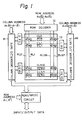
- Figure 1 is a block diagram of a memory device of the prior art;
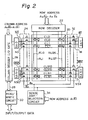
- Fig. 2 is a block diagram of an embodiment according to the present invention;
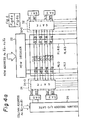
- Figs. 3a and 3b are waveform diagrams for explaining the read/write operation of the embodiment of Fig. 2;
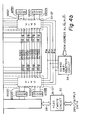
- Fig. 4 which is separately illustrated as Figs. 4a and 4b is a block diagram of another embodiment according to the present invention; and
- Fig. 5 is a circuit diagram of a part of the embodiment of Fig. 4.
- Before describing a memory device of the present invention, a prior art memory device will be described for reference purposes.
- Figure 1 illustrates a dynamic memory device with a storage capacity of 64 kbits according to the prior art. In Fig. 1,
reference numeral 10 indicates one of a plurality of single element type storage cells arrayed in 128 rows and 512 columns, and 12 a row decoder (word decoder) coupled to each of row lines (word lines) RLO to RL127. Reference symbols CLO and CLO to CL511 and CL511 indicate pairs of column lines (bit lines). Sense amplifiers SAO to SA511 are connected to each pair of the column lines. The sense amplifiers SAO, SA2, ---, and SA510 indicated by even numbers are disposed on the left side of the storage cell array in Fig. 1, and the sense amplifiers SA1, SA3, ---, and SA511 indicated by odd numbers are disposed on the right side. That is, the sense amplifiers are alternately disposed on opposite sides of the array. Therefore, twice the usual pitch space is available for each sense amplifier, enabling the pitch to be further narrowed without making disposition of the sense amplifiers difficult. - However, as mentioned before, such a memory device requires two column decoders and I/
O gate circuits - Figure 2 illustrates an embodiment of the present invention. In Fig. 2, reference numeral 20-indicates one of a plurality of single element storage cells arrayed in 128 rows and in 512 columns. Each of the metal-oxide-semiconductor field effect transistor (MOSFET) storage cells is composed of one / and a capacitor. In Fig. 2, furthermore, reference symbols RLO to RL127 indicate row lines (word lines). CLO and CLO to CL511 and CL511 indicate pairs of column lines (bit lines) crossing the row lines RLO to RL127. Each of the storage cells is connected to one of the row lines RLO to RL127 and to one of the column lines CLO to CL511 and CLO to CL511 at the crossing points.
- A row decoder (word decoder) 22 is coupled to the end of the row lines RLO to RL127 and selects one of 128 row lines in accordance with an upper 7 bit address A0A0 to A6A6 of the row address A0
A 0 to A-A-. - One of the ends of the column lines CLO to CL511 and CLO to CL511 can be coupled to sense amplifiers indicated by even numbers SAO SA2, ---, SA508 and SA510 via bidirectional transfer gate elements composed of FET's.
Reference numeral 24 in Fig. 2 indicates a gate circuit including these gate elements. Each of the sense amplifiers SAO, SA2, ---, and SA510, which includes a bistable circuit and an active pull-up circuit, is coupled to two pairs of the column lines. For example, two pairs of the column lines CLO and CLO, CL1 and CL1 are coupled to SAO, and CL2 and CL2, CL3 and CL3 are coupled to SA2. The sense amplifiers SAO, SA2, ---, and SA510 are also connected to a column decoder (bit decoder) and I/O gate circuit 26. The column decoder and I/O gate circuit 26 select one of 256 column lines in accordance with column address A0A0 to A-A- , and transfer information from the selected column lines, namely, from the selected storage cell to a read/writecircuit 30 via abus line 28. The column decoder and I/O gate circuit 26 also transfers information from the read/write circuit 30 to the selected storage cell. - The other ends of the column lines CLO to CL511 and CLO to CL511 can be coupled to sense amplifiers indicated by odd numbers SA1, SA3, ---, and SA511, via bidirectional transfer gate elements also composed of FET's. In Fig. 2,
reference numeral 32 denotes a gate circuit including these gate elements. Each of the sense amplifiers SA1, SA3, ---, and SA511, which include a bistable circuit and an active pull-up circuit, is coupled to two pairs of the column lines as well as the aforementioned sense amplifiers SAO, SA2, ---, and SA510. However, these sense amplifiers SA1, SA3, ---, and SA511 are not connected to a column decoder. Information detected by these sense amplifiers SA1, SA3, ---, and SA511 is amplified and then written back to the original storage cell without being output. In other words, these sense amplifiers SA1, SA3, ---, and SA511 are provided for refreshing the storage cells. - Each gate element (FET) in the
gate circuits amplifier selection circuit 34, and thus turns on or off in response to selection signals φS and φS from the senseamplifier selection circuit 34. The senseamplifier selection circuit 34 produces the selection signals φS and φS depending upon the least significant bit (LSB) A7 andA 7 of the row address. - When the selection signal φS is the "H" level and the other selection signal φS is the "L" level, pairs of the even number column lines CLO and CLO, CL2 and CL2, ---, and CL510 and CL510 are communicated with the sense amplifiers SAO, SA2, ---, and SA510 indicated in the left side in Fig. 2, and pairs of the odd number column lines CL1 and CL1, CL3 and CL3, ---, and CL511 and CL511 are communicated to the sense amplifiers SA1, SA3, ---, and SA511 indicated in the right side in Fig. 2. Therefore, in this case, information on the pairs of the even number column lines CLO and CLO, CL2 and CL2, ---, and CL510 and CL510 is detected by the sense amplifiers BA0, SA2, ---, and SA510 and then fed to the column Mecoder and I/
O gate circuit 26. The column decoder and I/O gate circuit 26 selects one of the 256 column lines and obtains information on a desired column line or writes information to a storage cell on a desired column line. Meanwhile, s information on the pairs of the odd number column lines CL1 and CL1, CL3 and CL3, ---, and CL511 and CL511 is refreshed by the sense amplifiers SA1, SA3, --- and SA511. - In contrast with this, when the selection signal φS is the "L" level and φS is the "H" level, information on the pairs of the odd number column lines CL1 and CL1, CL3 and CL3, ---, and CL511 and CL511 is read or written.
- Figures 3a and 3b illustrate waveforms of various present during operation of signals / the embodiment of Fig. 2. The now read/write operation of the embodiment of Fig. 2 will/be explained.
- At a time t, , the row addresses A0A0 to A7A7 are given. Then, at a time t2 , a single row line is selected (the voltage on a selected row line RL rises) by the
row decoder 22. At the same time, the selection signal φS rises to the "H" level, which is a voltage above a writing voltage of the storage cell. The writing voltage is more than a supply voltage VCC. - Thus, the column lines are communicated to the sense amplifiers. At a time t3 , information is output from the storage cells coupled to the selected row line to the respective column lines, causing the differential voltages between the pairs of the column lines CLO and CLO, CL1 and CL1, ---, and CL511 and CL511. At this time, since the selection signal φS has risen enough, the differential voltages are applied to the sense amplifiers SA0, SA, , ---, and SA511, respectively without a time delay. In this case, since the selection signal φS is the "H" level, pairs of the even number column lines are communicated with the even number sense amplifiers, and pairs of the odd number column lines are commnicated with the odd number sense amplifiers. For instance, the pair of column lines CLO and CLO is communicated with the sense amplifier SAO, and the pair of column lines CL1 and CL1 is communicated with the sense amplifier SAl.
- At a time t4, the sense amplifiers start to amplify the applied differential voltages. Thus, the to a voltage nodes N0, N0, Nl, N1 are charged or discharged to VCC or/ VSS. For instance, as shown in Fig. 3b, the nodes NO and N1 are charged to VCC and the nodes NO and N1 are discharged to VSS. These amplified voltages are written to the storage cells via the respective column lines. Thus, the refresh operation of the storage cells is achieved It should be noted that, in this case (φS= "H"), the storage cells communicated with the column lines CLO and CLO are refreshed by the sense amplifier SAO, and the storage cells communicated with the column lines CLl and CL1 are refreshed by the sense amplifier SAl which is exclusively used for a refreshing operation. At the time t4 , furthermore, the column addresses A0A0 to A7A7 are given. Thus, one of the information developed at the nodes N0, N0, N2, N2, ---, N510, and N510 is selected. The selected information is fed to the
data bus 28 at a time t5. - Figure 4 (Figs. 4a and 4b) illustrates another embodiment of the present invention, and Fig. 5 illustrates in detail a part of the gate circuits in the embodiment of Fig. 4.
- In this embodiment, the storage cell array is coupled to 64 row lines and to 1024 column lines. One quarter of the 1024 sense amplifiers are connected to a column decoder and I/
O gate circuit 26. The remaining sense amplifiers are exclusively used for refreshihg. For instance, a sense amplifier SAO is connected to the column decoder and I/O gate circuit 26, but sense amplifiers SA1, SA2, and SA3 are not connected to the column decoder. Therefore, one of the pairs of the column lines CLO and CLO, CL1 and CL1, CL2 and CL2, and CL3 and CL3 is communicated to the sense amplifier SAO and thus communicated to the column decoder. The other pairs of the column lines are communicated to the sense amplifiers SA1, SA2, and SA3 to execute only the refresh operation. This selection of pairs of the column lines is executed bygate circuits gate circuits amplifier selection circuit 34. The senseamplifier selection circuit 34 produces the selection signal φS0 to φS3 in response to the lower two bits A6A 6 and A7A7 of the row address. - Since the operation of this latter embodiment is similar to the former embodiment, a detailed explanation of the operation is omitted.
- Many widely different embodiments of the present invention may be constructed without departing from the spirit and scope of the present invention. It should be understood that the present invention is not limited to the specific embodiments described in this specification, except as defined in the appended claims.
Claims (9)
Applications Claiming Priority (2)
| Application Number | Priority Date | Filing Date | Title |
|---|---|---|---|
| JP167522/82 | 1982-09-28 | ||
| JP57167522A JPS5958689A (en) | 1982-09-28 | 1982-09-28 | Semiconductor storage device |
Publications (2)
| Publication Number | Publication Date |
|---|---|
| EP0107387A2 true EP0107387A2 (en) | 1984-05-02 |
| EP0107387A3 EP0107387A3 (en) | 1986-10-15 |
Family
ID=15851251
Family Applications (1)
| Application Number | Title | Priority Date | Filing Date |
|---|---|---|---|
| EP83305837A Withdrawn EP0107387A3 (en) | 1982-09-28 | 1983-09-28 | Semiconductor memory device |
Country Status (3)
| Country | Link |
|---|---|
| US (1) | US4581720A (en) |
| EP (1) | EP0107387A3 (en) |
| JP (1) | JPS5958689A (en) |
Families Citing this family (22)
| Publication number | Priority date | Publication date | Assignee | Title |
|---|---|---|---|---|
| US4630240A (en) * | 1984-07-02 | 1986-12-16 | Texas Instruments Incorporated | Dynamic memory with intermediate column derode |
| JPS6134792A (en) * | 1984-07-25 | 1986-02-19 | Toshiba Corp | Semiconductor memory device |
| US4800525A (en) * | 1984-10-31 | 1989-01-24 | Texas Instruments Incorporated | Dual ended folded bit line arrangement and addressing scheme |
| JPS61242396A (en) * | 1985-04-19 | 1986-10-28 | Nec Corp | Semiconductor memory |
| US5197033A (en) | 1986-07-18 | 1993-03-23 | Hitachi, Ltd. | Semiconductor device incorporating internal power supply for compensating for deviation in operating condition and fabrication process conditions |
| US4710902A (en) * | 1985-10-04 | 1987-12-01 | Motorola, Inc. | Technique restore for a dynamic random access memory |
| US4807194A (en) * | 1986-04-24 | 1989-02-21 | Matsushita Electric Industrial Co., Ltd. | Seimiconductor memory device having sub bit lines |
| JPS63104296A (en) * | 1986-10-21 | 1988-05-09 | Nec Corp | Semiconductor memory device |
| JPS63205897A (en) * | 1987-02-20 | 1988-08-25 | Matsushita Electric Ind Co Ltd | Semiconductor storage device |
| US5222047A (en) * | 1987-05-15 | 1993-06-22 | Mitsubishi Denki Kabushiki Kaisha | Method and apparatus for driving word line in block access memory |
| US5280448A (en) * | 1987-11-18 | 1994-01-18 | Sony Corporation | Dynamic memory with group bit lines and associated bit line group selector |
| JPH01158694A (en) * | 1987-12-15 | 1989-06-21 | Mitsubishi Electric Corp | Semiconductor dynamic ram |
| EP0321847B1 (en) * | 1987-12-21 | 1994-06-29 | Kabushiki Kaisha Toshiba | Semiconductor memory capable of improving data rewrite speed |
| JP2691280B2 (en) * | 1988-05-12 | 1997-12-17 | 三菱電機株式会社 | Semiconductor memory device |
| JPH0271493A (en) * | 1988-09-06 | 1990-03-12 | Mitsubishi Electric Corp | Semiconductor memory device |
| JP2633645B2 (en) * | 1988-09-13 | 1997-07-23 | 株式会社東芝 | Semiconductor memory device |
| US5034920A (en) * | 1988-10-12 | 1991-07-23 | Texas Instruments Incorporated | Cross point array memory device |
| JP2723683B2 (en) * | 1991-02-25 | 1998-03-09 | 日本電気アイシーマイコンシステム株式会社 | Semiconductor storage device |
| US5465339A (en) * | 1991-02-27 | 1995-11-07 | Vlsi Technology, Inc. | Decoupled refresh on local and system busses in a PC/at or similar microprocessor environment |
| US5291443A (en) * | 1991-06-26 | 1994-03-01 | Micron Technology, Inc. | Simultaneous read and refresh of different rows in a dram |
| US5636158A (en) * | 1995-03-13 | 1997-06-03 | Kabushiki Kaisha Toshiba | Irregular pitch layout for a semiconductor memory device |
| JPH10241354A (en) * | 1997-02-21 | 1998-09-11 | Mitsubishi Electric Corp | Bidirectional transfer type memory and input-output control method for memory |
Citations (2)
| Publication number | Priority date | Publication date | Assignee | Title |
|---|---|---|---|---|
| US3599180A (en) * | 1968-11-29 | 1971-08-10 | Gen Instrument Corp | Random access read-write memory system having data refreshing capabilities and memory cell therefor |
| DE3048105A1 (en) * | 1979-12-21 | 1981-09-24 | Hitachi, Ltd., Tokyo | STORAGE |
Family Cites Families (2)
| Publication number | Priority date | Publication date | Assignee | Title |
|---|---|---|---|---|
| JPS6048074B2 (en) * | 1978-02-09 | 1985-10-25 | 日本電気株式会社 | memory circuit |
| US4203159A (en) * | 1978-10-05 | 1980-05-13 | Wanlass Frank M | Pseudostatic electronic memory |
-
1982
- 1982-09-28 JP JP57167522A patent/JPS5958689A/en active Pending
-
1983
- 1983-09-26 US US06/535,836 patent/US4581720A/en not_active Expired - Fee Related
- 1983-09-28 EP EP83305837A patent/EP0107387A3/en not_active Withdrawn
Patent Citations (2)
| Publication number | Priority date | Publication date | Assignee | Title |
|---|---|---|---|---|
| US3599180A (en) * | 1968-11-29 | 1971-08-10 | Gen Instrument Corp | Random access read-write memory system having data refreshing capabilities and memory cell therefor |
| DE3048105A1 (en) * | 1979-12-21 | 1981-09-24 | Hitachi, Ltd., Tokyo | STORAGE |
Non-Patent Citations (2)
| Title |
|---|
| IBM TECHNICAL DISCLOSURE BULLETIN, vol. 23, no. 10, March 1981, pages 4620,4621, P.T. WU: "Read/write dynamic memory using two devices per cell and having internal refresh" * |
| IBM TECHNICAL DISCLOSURE BULLETIN, vol. 24, no. 10, March 1982, pages 5242-5244; P.C. TIEN: "Differential sense amplifier for unbalanced data lines" * |
Also Published As
| Publication number | Publication date |
|---|---|
| US4581720A (en) | 1986-04-08 |
| JPS5958689A (en) | 1984-04-04 |
| EP0107387A3 (en) | 1986-10-15 |
Similar Documents
| Publication | Publication Date | Title |
|---|---|---|
| EP0107387A2 (en) | Semiconductor memory device | |
| US5111434A (en) | Semiconductor memory device | |
| EP0068645B1 (en) | A semiconductor device | |
| US5970006A (en) | Semiconductor memory device having cell array divided into a plurality of cell blocks | |
| US4367540A (en) | Dynamic memory with an interchangeable pair of data lines and sense amplifiers | |
| KR100824798B1 (en) | Memory core capable of writing a full data pattern to edge sub arrays, semiconductor memory device having the same, and method for testing edge sub arrays | |
| US4086662A (en) | Memory system with read/write control lines | |
| US5418750A (en) | Semiconductor memory device for suppressing noises occurring on bit and word lines | |
| US4920517A (en) | Semiconductor memory device having sub bit lines | |
| US4418399A (en) | Semiconductor memory system | |
| EP0107340B1 (en) | Dual port type semiconductor memory | |
| US4680734A (en) | Semiconductor memory device | |
| US5862072A (en) | Memory array architecture and method for dynamic cell plate sensing | |
| KR940006996B1 (en) | Semiconductor memory device | |
| JPH05342855A (en) | Semiconductor memory circuit | |
| US5305258A (en) | Semiconductor memory and memory cell | |
| US4511997A (en) | Semiconductor memory device | |
| JPH02247890A (en) | Semiconductor memory device | |
| KR19980019221A (en) | Semiconductor storage device | |
| KR100207536B1 (en) | Semiconductor memory device having data masking function | |
| US4389714A (en) | Memory device | |
| US6058067A (en) | Multi-bank semiconductor memory device having an output control circuit for controlling bit line pairs of each bank connected to data bus pairs | |
| KR950002042A (en) | Dynamic random access memory device having first and second input / output line groups separated from each other | |
| US5337287A (en) | Dual port semiconductor memory device | |
| KR100267132B1 (en) | Semicondutor memory device |
Legal Events
| Date | Code | Title | Description |
|---|---|---|---|
| PUAI | Public reference made under article 153(3) epc to a published international application that has entered the european phase |
Free format text: ORIGINAL CODE: 0009012 |
|
| AK | Designated contracting states |
Designated state(s): DE FR GB |
|
| PUAL | Search report despatched |
Free format text: ORIGINAL CODE: 0009013 |
|
| AK | Designated contracting states |
Kind code of ref document: A3 Designated state(s): DE FR GB |
|
| 17P | Request for examination filed |
Effective date: 19870327 |
|
| 17Q | First examination report despatched |
Effective date: 19880115 |
|
| STAA | Information on the status of an ep patent application or granted ep patent |
Free format text: STATUS: THE APPLICATION HAS BEEN WITHDRAWN |
|
| 18W | Application withdrawn |
Withdrawal date: 19900329 |
|
| R18W | Application withdrawn (corrected) |
Effective date: 19900329 |
|
| RIN1 | Information on inventor provided before grant (corrected) |
Inventor name: SATO, KIMIAKI Inventor name: TAKEMAE, YOSHIHIRO Inventor name: NAKANO, TOMIO |