EP0106546A2 - Dual output power supply - Google Patents
Dual output power supply Download PDFInfo
- Publication number
- EP0106546A2 EP0106546A2 EP83305487A EP83305487A EP0106546A2 EP 0106546 A2 EP0106546 A2 EP 0106546A2 EP 83305487 A EP83305487 A EP 83305487A EP 83305487 A EP83305487 A EP 83305487A EP 0106546 A2 EP0106546 A2 EP 0106546A2
- Authority
- EP
- European Patent Office
- Prior art keywords
- voltage
- terminals
- capacitor
- circuit
- rectifier
- Prior art date
- Legal status (The legal status is an assumption and is not a legal conclusion. Google has not performed a legal analysis and makes no representation as to the accuracy of the status listed.)
- Granted
Links
Images
Classifications
-
- H—ELECTRICITY
- H02—GENERATION; CONVERSION OR DISTRIBUTION OF ELECTRIC POWER
- H02M—APPARATUS FOR CONVERSION BETWEEN AC AND AC, BETWEEN AC AND DC, OR BETWEEN DC AND DC, AND FOR USE WITH MAINS OR SIMILAR POWER SUPPLY SYSTEMS; CONVERSION OF DC OR AC INPUT POWER INTO SURGE OUTPUT POWER; CONTROL OR REGULATION THEREOF
- H02M7/00—Conversion of ac power input into dc power output; Conversion of dc power input into ac power output
- H02M7/02—Conversion of ac power input into dc power output without possibility of reversal
- H02M7/04—Conversion of ac power input into dc power output without possibility of reversal by static converters
- H02M7/06—Conversion of ac power input into dc power output without possibility of reversal by static converters using discharge tubes without control electrode or semiconductor devices without control electrode
-
- H—ELECTRICITY
- H02—GENERATION; CONVERSION OR DISTRIBUTION OF ELECTRIC POWER
- H02M—APPARATUS FOR CONVERSION BETWEEN AC AND AC, BETWEEN AC AND DC, OR BETWEEN DC AND DC, AND FOR USE WITH MAINS OR SIMILAR POWER SUPPLY SYSTEMS; CONVERSION OF DC OR AC INPUT POWER INTO SURGE OUTPUT POWER; CONTROL OR REGULATION THEREOF
- H02M1/00—Details of apparatus for conversion
- H02M1/0083—Converters characterised by their input or output configuration
- H02M1/009—Converters characterised by their input or output configuration having two or more independently controlled outputs
Definitions
- This invention relates to power supplies in general and more particularly relates to power supplies of this type for producing dual relatively high voltage outputs for electronic equipment.
- a typical application for this type of dual output power supply is a travelling wave tube which requires a high negative cathode voltage, say 3700 volts, at relatively low current with low ripple and good regulation, and a relatively low voltage, say 1900 volts, for the collector to cathode where the current is in the order of ten times the current at relatively high voltage, the ripple and regulation requirements for the lower voltage being much less stringent than for the higher voltage.
- a dual output power supply which includes a transformer having magnetically-coupled primary and secondary winding means; a rectifier-capacitor type first circuit energised by said secondary winding means to produce a first output voltage; a rectifier-capacitor type second circuit energised by said secondary winding means to produce a second output voltage referenced to said first output voltage; said first circuit including a first main capacitor across which said first output voltage appears and said second circuit including a second main capacitor across which said second output voltage appears; said secondary winding means including a common winding portion through which charging currents for both said first and second main capacitors flow, said charging current for said first main capacitor by-passing said second main capacitor, said charging current for said second main capacitor flowing through rectifier elements of said first circuit while by-passing said first main capacitor, and said second circuit having a voltage doubler type configuration.
- relatively low voltage output E b appearing between positive terminal 11 and common terminal 12 is produced by conventional rectifier bridge 14 having its input terminals 15 and 16 connected by the respective lines 17, 18 to the respective taps B, C of secondary winding 22.
- the latter is part of transformer Tl and is magnetically coupled to primary winding 21 of transformer Tl.
- Primary winding 21 is energised by A.C. input source 19.
- Bridge 14 also includes positive output terminal 31 connected directly to low voltage terminal 11 by conductor 33 and negative output terminal 32 connected directly to common terminal 12 by conductor 34.
- Main storage capacitor Cl is connected directly acrossa output terminals 31, 32.
- One charging path for capacitor Cl is through rectifiers CR1 and CR2, the former being connected between terminals 15 and 31 and the latter being connected between terminals 31 and 16.
- the other charging path for main capacitor Cl is through rectifiers CR3 and CR4, with rectifier CR3 being connected between terminals 16 and 31 and rectifier CR4 being connected between terminals 32 and 15.
- the load current between terminals 11, 12 is indicated by the broken line I b .
- the relatively high voltage output E a appears between common terminal 12 and positive grounded terminal 35.
- the latter is connected by conductor 36 to the positive terminal of main storage capacitor C4 whose negative terminal is connected through line 34 to common terminal 12.
- the path for high voltage load current is indicated by the dashed line I . a
- Secondary winding 22 of transformer Tl also includes terminal A located outboard of terminal B, and terminal D located outboard of terminal C.
- terminal A When terminal A is positive, main capacitor C4 is charged through a circuit consisting of line 17 connected to terminal B, auxiliary capacitor C3, charging rectifier CRB, rectifier element CR2 of bridge 14, and conductor 18 to transformer terminal C. While this is occurring, auxiliary capacitor C2 is being charged through auxiliary rectifier CR5 to the voltage appearing between terminals A and C.
- main capacitor C4 When the polarity on transformer winding 22 reverses, that is when terminal D is positive with respect to terminal A, the charging path for main capacitor C4 extends between terminals B and C and consists of line 18 extending from terminal C, auxiliary capacitor C2, charging rectifier CR6, and rectifier element CR4 of bridge 14 connected by conductor 17 to terminal B. While this is occurring, auxiliary capacitor C3 is being charged through auxiliary rectifier CR7 to the voltage appearing between transformer terminals B and D.
- main storage capacitor C4 is charghed by a potential equal to the algebraic sum of the voltage between terminals A and B and twice the voltage between terminals B and C. It should now be apparent to those skilled in the art that main capacitor C4 is part of what can be termed a voltage doubler type circuit.
- High voltage output E may be increased by increasing the voltage between terminals A and C maintaining this voltage substantially equal to the voltage between terminals B and D.
- high voltage E a may be decreased by decreasing the voltages between winding terminals AC and BD.
- the voltages E a and E b will be equal when the voltages across each of the auxiliary capacitors C2 and C3 is equal to approximately one half the output voltage of bridge 14. It is noted that the circuit hereinbefore described will work equally as well while producing a higher voltage between terminals 12 and 35 if the connection from auxiliary capacitor C2 to terminal C is moved to terminal to terminal D and the connection from auxiliary capacitor C3 to terminal B is moved to terminal A.
- circuit illustrated may be modified as follows:
Landscapes
- Engineering & Computer Science (AREA)
- Power Engineering (AREA)
- Rectifiers (AREA)
- Dc-Dc Converters (AREA)
Abstract
Description
- This invention relates to power supplies in general and more particularly relates to power supplies of this type for producing dual relatively high voltage outputs for electronic equipment.
- In the construction of modern electronic equipment requiring relatively high voltage, size reduction and a reduction in the number of components used are primary considerations which the prior art has found difficulty in dealing with. In particular, difficulties have arisen when constructing power supplies having relatively high and low voltage outputs that are referenced to one another and in which the current delivered by the low voltage output is many times greater than the current delivered by the high voltage output especially when requirements of low ripple and good voltage regulation are required of the higher output- voltage. A typical application for this type of dual output power supply is a travelling wave tube which requires a high negative cathode voltage, say 3700 volts, at relatively low current with low ripple and good regulation, and a relatively low voltage, say 1900 volts, for the collector to cathode where the current is in the order of ten times the current at relatively high voltage, the ripple and regulation requirements for the lower voltage being much less stringent than for the higher voltage.
- In order to produce the foregoing type output voltages the prior art has often taken a brute force approach in which the transformer supplying energy to the power supply is provided with individual secondary windings that are totally isolated from one another to produce the individual output voltages. In an attempt to economise on transformer size, the prior art has also provided circuit configurations wherein a common secondary winding is utilised in producing both output voltages. However, this has proven to be wasteful in terms of the number of components, principally because blocking capacitors must be included, and perhaps more importantly rectifier components sizes have been excessive especially when the voltages being produced are in excess of 600 volts. The latter problem increases when the ripple and regulation requirements of the higher voltage output are much greater than for the lower voltage output, and the problem becomes more difficult of solution when the current requirements for the lower voltage output are many times greater than the higher voltage output.
- It is an object of the present invention to provide a dual-output high voltage power supply in which the above problems of size and rating of components are avoided.
- According to the present invention there is provided a dual output power supply which includes a transformer having magnetically-coupled primary and secondary winding means; a rectifier-capacitor type first circuit energised by said secondary winding means to produce a first output voltage; a rectifier-capacitor type second circuit energised by said secondary winding means to produce a second output voltage referenced to said first output voltage; said first circuit including a first main capacitor across which said first output voltage appears and said second circuit including a second main capacitor across which said second output voltage appears; said secondary winding means including a common winding portion through which charging currents for both said first and second main capacitors flow, said charging current for said first main capacitor by-passing said second main capacitor, said charging current for said second main capacitor flowing through rectifier elements of said first circuit while by-passing said first main capacitor, and said second circuit having a voltage doubler type configuration.
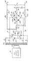
- The invention will now be described with reference to the drawing, which shows an electrical circuit diagram of a dual-voltage power supply.
- Now referring to the drawing, relatively low voltage output Eb appearing between
positive terminal 11 and common terminal 12 is produced byconventional rectifier bridge 14 having itsinput terminals 15 and 16 connected by therespective lines 17, 18 to the respective taps B, C of secondary winding 22. The latter is part of transformer Tl and is magnetically coupled to primary winding 21 of transformer Tl.Primary winding 21 is energised byA.C. input source 19.Bridge 14 also includespositive output terminal 31 connected directly tolow voltage terminal 11 byconductor 33 andnegative output terminal 32 connected directly to common terminal 12 byconductor 34. Main storage capacitor Cl is connected directly acrossaoutput terminals terminals terminals 31 and 16. The other charging path for main capacitor Cl is through rectifiers CR3 and CR4, with rectifier CR3 being connected betweenterminals 16 and 31 and rectifier CR4 being connected betweenterminals terminals 11, 12 is indicated by the broken line Ib. - The relatively high voltage output E a appears between common terminal 12 and positive
grounded terminal 35. The latter is connected byconductor 36 to the positive terminal of main storage capacitor C4 whose negative terminal is connected throughline 34 to common terminal 12. The path for high voltage load current is indicated by the dashed line I . a - Secondary winding 22 of transformer Tl also includes terminal A located outboard of terminal B, and terminal D located outboard of terminal C. When terminal A is positive, main capacitor C4 is charged through a circuit consisting of line 17 connected to terminal B, auxiliary capacitor C3, charging rectifier CRB, rectifier element CR2 of
bridge 14, andconductor 18 to transformer terminal C. While this is occurring, auxiliary capacitor C2 is being charged through auxiliary rectifier CR5 to the voltage appearing between terminals A and C. When the polarity on transformer winding 22 reverses, that is when terminal D is positive with respect to terminal A, the charging path for main capacitor C4 extends between terminals B and C and consists ofline 18 extending from terminal C, auxiliary capacitor C2, charging rectifier CR6, and rectifier element CR4 ofbridge 14 connected by conductor 17 to terminal B. While this is occurring, auxiliary capacitor C3 is being charged through auxiliary rectifier CR7 to the voltage appearing between transformer terminals B and D. - The voltage between transformer terminals A and B is equal to the voltage between transformer terminals C and D. Thus, main storage capacitor C4 is charghed by a potential equal to the algebraic sum of the voltage between terminals A and B and twice the voltage between terminals B and C. It should now be apparent to those skilled in the art that main capacitor C4 is part of what can be termed a voltage doubler type circuit. High voltage output E may be increased by increasing the voltage between terminals A and C maintaining this voltage substantially equal to the voltage between terminals B and D. Conversely, high voltage E a may be decreased by decreasing the voltages between winding terminals AC and BD. The voltages Ea and Eb will be equal when the voltages across each of the auxiliary capacitors C2 and C3 is equal to approximately one half the output voltage of
bridge 14. It is noted that the circuit hereinbefore described will work equally as well while producing a higher voltage betweenterminals 12 and 35 if the connection from auxiliary capacitor C2 to terminal C is moved to terminal to terminal D and the connection from auxiliary capacitor C3 to terminal B is moved to terminal A. - To achieve other voltage relationships, the circuit illustrated may be modified as follows:
- (1) For voltage Eb to be a negative voltage referenced to the positive output terminal of E , all of the rectifier polarities must be reversed.
- (2) For voltages E to be positive and referenced to ground and voltage E, to be positive with reference to ground, the connections of
output lines - (3) To have voltage Eb negative and voltage E negative and with both of these voltages referenced to ground, interchange the connections of
output lines - (4) To change the reference point of those circuits described above in which voltage Eb is referenced to voltage E , by moving ground from
terminal 35 to aterminal 11 voltage Ea will be referenced to voltage Eb. - It should now be apparent to those skilled in the art that by eliminating main capacitor Cl and bridge rectifier elements CR1 and CR3 the remaining circuit is effectively a voltage doubler. Although the output voltage between
terminals 12 and 35 will not be precisely twice the voltage between transformer terminals BC but is also a function of the potential between terminals AB and CD. - Although a preferred embodiment of this invention has been described, many variations and modifications will now be apparent to those skilled in the art, and it is therefore preferred that the instant invention be limited not by the specific disclosure herein, but only by the appending claims.
Claims (7)
Applications Claiming Priority (2)
| Application Number | Priority Date | Filing Date | Title |
|---|---|---|---|
| US429449 | 1982-09-30 | ||
| US06/429,449 US4442482A (en) | 1982-09-30 | 1982-09-30 | Dual output H.V. rectifier power supply driven by common transformer winding |
Publications (3)
| Publication Number | Publication Date |
|---|---|
| EP0106546A2 true EP0106546A2 (en) | 1984-04-25 |
| EP0106546A3 EP0106546A3 (en) | 1984-10-17 |
| EP0106546B1 EP0106546B1 (en) | 1987-09-02 |
Family
ID=23703303
Family Applications (1)
| Application Number | Title | Priority Date | Filing Date |
|---|---|---|---|
| EP83305487A Expired EP0106546B1 (en) | 1982-09-30 | 1983-09-19 | Dual output power supply |
Country Status (3)
| Country | Link |
|---|---|
| US (1) | US4442482A (en) |
| EP (1) | EP0106546B1 (en) |
| DE (1) | DE3373389D1 (en) |
Families Citing this family (2)
| Publication number | Priority date | Publication date | Assignee | Title |
|---|---|---|---|---|
| GB2176918B (en) * | 1985-06-13 | 1989-11-01 | Intel Corp | Memory management for microprocessor system |
| US5742490A (en) * | 1996-10-29 | 1998-04-21 | Electronic Measurements, Inc. | Power converter having a configurable output stage |
Citations (3)
| Publication number | Priority date | Publication date | Assignee | Title |
|---|---|---|---|---|
| US2704332A (en) * | 1952-12-11 | 1955-03-15 | Hughes Aircraft Co | Modified bridge rectifier circuit |
| US4109306A (en) * | 1977-10-06 | 1978-08-22 | Teccor Electronics, Inc. | Power supply |
| JPS5771272A (en) * | 1980-10-17 | 1982-05-04 | Hitachi Ltd | Rectifying circuit |
-
1982
- 1982-09-30 US US06/429,449 patent/US4442482A/en not_active Expired - Fee Related
-
1983
- 1983-09-19 DE DE8383305487T patent/DE3373389D1/en not_active Expired
- 1983-09-19 EP EP83305487A patent/EP0106546B1/en not_active Expired
Patent Citations (3)
| Publication number | Priority date | Publication date | Assignee | Title |
|---|---|---|---|---|
| US2704332A (en) * | 1952-12-11 | 1955-03-15 | Hughes Aircraft Co | Modified bridge rectifier circuit |
| US4109306A (en) * | 1977-10-06 | 1978-08-22 | Teccor Electronics, Inc. | Power supply |
| JPS5771272A (en) * | 1980-10-17 | 1982-05-04 | Hitachi Ltd | Rectifying circuit |
Non-Patent Citations (1)
| Title |
|---|
| Patent Abstracts of Japan vol. 6, no. 147, 6 August 1982 & JP-A-57-71272 * |
Also Published As
| Publication number | Publication date |
|---|---|
| US4442482A (en) | 1984-04-10 |
| DE3373389D1 (en) | 1987-10-08 |
| EP0106546A3 (en) | 1984-10-17 |
| EP0106546B1 (en) | 1987-09-02 |
Similar Documents
| Publication | Publication Date | Title |
|---|---|---|
| US5057990A (en) | Bidirectional switching power apparatus with AC or DC output | |
| US5200887A (en) | Power supply unit for arc processing | |
| US5798630A (en) | Switching power circuit to supply electric-vehicle battery charger with high-frequency power | |
| US3846695A (en) | Series-parallel dual switching regulator for use with a variety of line voltages | |
| US4498127A (en) | Static converter with electric valves comprising a twelve-phase connection with two Graetz bridges for the suppression of harmonics 5 and 7 of network current | |
| US4675795A (en) | Step-up rectifier circuit | |
| EP0106546B1 (en) | Dual output power supply | |
| EP0964504B1 (en) | Switching power source apparatus | |
| US4422139A (en) | Transformer coupled up-down converter | |
| US3849701A (en) | Integrated dual voltage power supply | |
| JPH06141536A (en) | Low-loss power supply device including dc/dc converter | |
| US3292073A (en) | Voltage-multiplier rectifier circuits | |
| JP2861430B2 (en) | Rectifier circuit | |
| US4224661A (en) | Externally commutated compensation-type converter system and method of forced commutation and blocking of rectifiers thereof | |
| GB2127631A (en) | Multiple step-up rectifier circuit | |
| US2320224A (en) | Rectifier circuit | |
| US3609510A (en) | Rectifying bridge employed for dc electric transmission line | |
| SU847463A1 (en) | Ac-to-dc voltage converter | |
| SU684674A1 (en) | Device for power supply of load | |
| EP0589204B1 (en) | Improvement in a stabilized-voltage power supply circuit for boost converters | |
| SU1734176A1 (en) | Ac voltage-to-dc voltage converter | |
| JPS6124913B2 (en) | ||
| SU898571A1 (en) | Ac-to-dc voltage converter | |
| JPH0341892Y2 (en) | ||
| JP2538699Y2 (en) | Full bridge type inverter |
Legal Events
| Date | Code | Title | Description |
|---|---|---|---|
| PUAI | Public reference made under article 153(3) epc to a published international application that has entered the european phase |
Free format text: ORIGINAL CODE: 0009012 |
|
| AK | Designated contracting states |
Designated state(s): DE FR GB SE |
|
| PUAL | Search report despatched |
Free format text: ORIGINAL CODE: 0009013 |
|
| AK | Designated contracting states |
Designated state(s): DE FR GB SE |
|
| 17P | Request for examination filed |
Effective date: 19841105 |
|
| GRAA | (expected) grant |
Free format text: ORIGINAL CODE: 0009210 |
|
| AK | Designated contracting states |
Kind code of ref document: B1 Designated state(s): DE FR GB SE |
|
| ET | Fr: translation filed | ||
| REF | Corresponds to: |
Ref document number: 3373389 Country of ref document: DE Date of ref document: 19871008 |
|
| PLBE | No opposition filed within time limit |
Free format text: ORIGINAL CODE: 0009261 |
|
| STAA | Information on the status of an ep patent application or granted ep patent |
Free format text: STATUS: NO OPPOSITION FILED WITHIN TIME LIMIT |
|
| 26N | No opposition filed | ||
| PG25 | Lapsed in a contracting state [announced via postgrant information from national office to epo] |
Ref country code: GB Effective date: 19890919 |
|
| PG25 | Lapsed in a contracting state [announced via postgrant information from national office to epo] |
Ref country code: SE Effective date: 19890920 |
|
| GBPC | Gb: european patent ceased through non-payment of renewal fee | ||
| PG25 | Lapsed in a contracting state [announced via postgrant information from national office to epo] |
Ref country code: FR Effective date: 19900531 |
|
| PG25 | Lapsed in a contracting state [announced via postgrant information from national office to epo] |
Ref country code: DE Effective date: 19900601 |
|
| REG | Reference to a national code |
Ref country code: FR Ref legal event code: ST |
|
| EUG | Se: european patent has lapsed |
Ref document number: 83305487.7 Effective date: 19900521 |